Paper Menu >>
Journal Menu >>
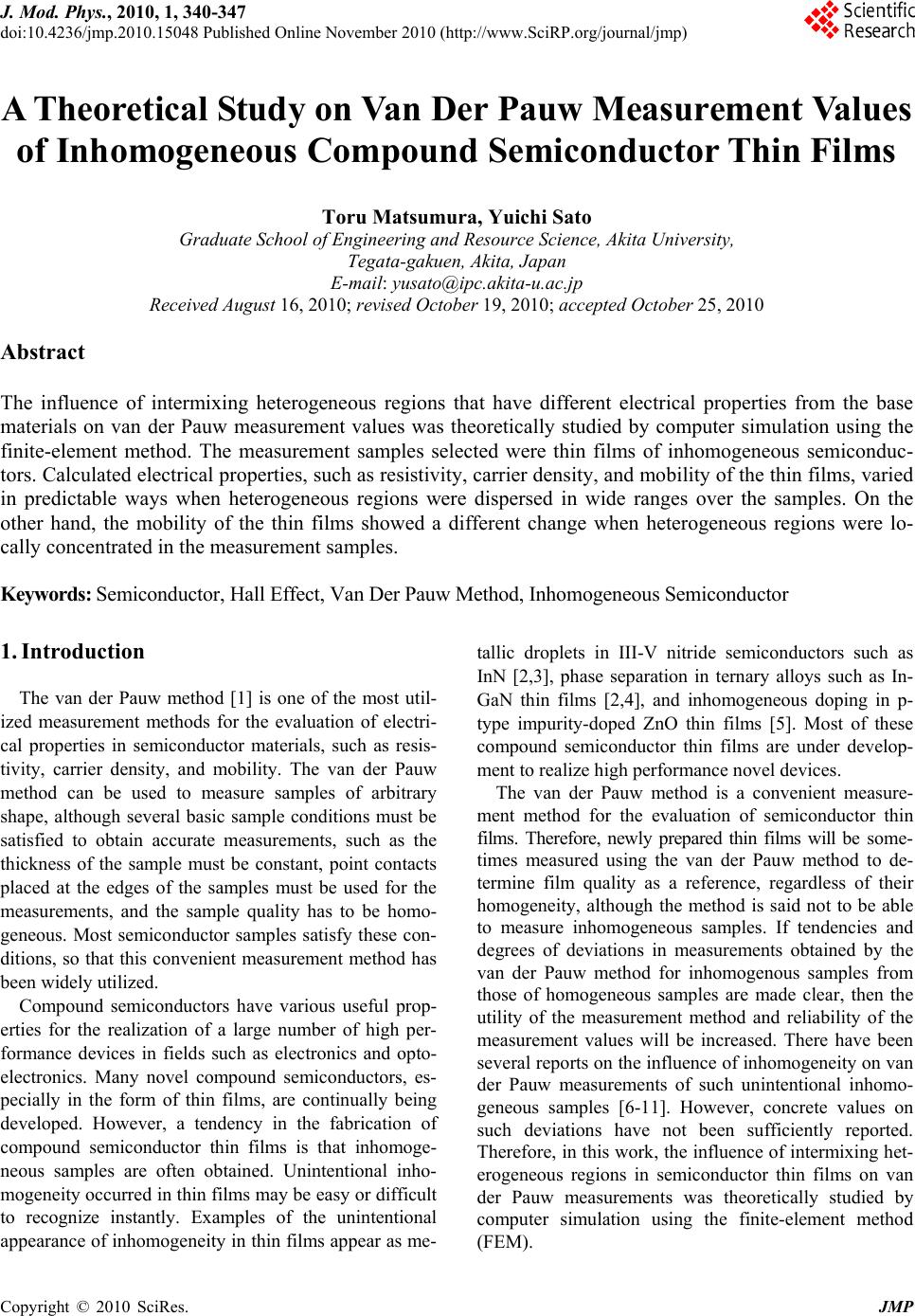 J. Mod. Phys., 2010, 1, 340-347 doi:10.4236/jmp.2010.15048 Published Online November 2010 (http://www.SciRP.org/journal/jmp) Copyright © 2010 SciRes. JMP A Theoretical Study on Van Der Pauw Measurement Values of Inhomogeneous Compound Semiconductor Thin Films Toru Matsumura, Yuichi Sato Graduate School of Engineering and Resource Science, Akita University, Tegata-gakuen, Akita, Japan E-mail: yusato@ipc.akita-u.ac.jp Received August 16, 2010; revised October 19, 2010; accepted October 25, 2010 Abstract The influence of intermixing heterogeneous regions that have different electrical properties from the base materials on van der Pauw measurement values was theoretically studied by computer simulation using the finite-element method. The measurement samples selected were thin films of inhomogeneous semiconduc- tors. Calculated electrical properties, such as resistivity, carrier density, and mobility of the thin films, varied in predictable ways when heterogeneous regions were dispersed in wide ranges over the samples. On the other hand, the mobility of the thin films showed a different change when heterogeneous regions were lo- cally concentrated in the measurement samples. Keywords: Semiconductor, Hall Effect, Van Der Pauw Method, Inhomogeneous Semiconductor 1. Introduction The van der Pauw method [1] is one of the most util- ized measurement methods for the evaluation of electri- cal properties in semiconductor materials, such as resis- tivity, carrier density, and mobility. The van der Pauw method can be used to measure samples of arbitrary shape, although several basic sample conditions must be satisfied to obtain accurate measurements, such as the thickness of the sample must be constant, point contacts placed at the edges of the samples must be used for the measurements, and the sample quality has to be homo- geneous. Most semiconductor samples satisfy these con- ditions, so that this convenient measurement method has been widely utilized. Compound semiconductors have various useful prop- erties for the realization of a large number of high per- formance devices in fields such as electronics and opto- electronics. Many novel compound semiconductors, es- pecially in the form of thin films, are continually being developed. However, a tendency in the fabrication of compound semiconductor thin films is that inhomoge- neous samples are often obtained. Unintentional inho- mogeneity occurred in thin films may be easy or difficult to recognize instantly. Examples of the unintentional appearance of inhomogeneity in thin films appear as me- tallic droplets in III-V nitride semiconductors such as InN [2,3], phase separation in ternary alloys such as In- GaN thin films [2,4], and inhomogeneous doping in p- type impurity-doped ZnO thin films [5]. Most of these compound semiconductor thin films are under develop- ment to realize high performance novel devices. The van der Pauw method is a convenient measure- ment method for the evaluation of semiconductor thin films. Therefore, newly prepared thin films will be some- times measured using the van der Pauw method to de- termine film quality as a reference, regardless of their homogeneity, although the method is said not to be able to measure inhomogeneous samples. If tendencies and degrees of deviations in measurements obtained by the van der Pauw method for inhomogenous samples from those of homogeneous samples are made clear, then the utility of the measurement method and reliability of the measurement values will be increased. There have been several reports on the influence of inhomogeneity on van der Pauw measurements of such unintentional inhomo- geneous samples [6-11]. However, concrete values on such deviations have not been sufficiently reported. Therefore, in this work, the influence of intermixing het- erogeneous regions in semiconductor thin films on van der Pauw measurements was theoretically studied by computer simulation using the finite-element method (FEM).  T. MATSUMURA ET AL. Copyright © 2010 SciRes. JMP 341 2. Simulation Method Thin film compound semiconductors were selected as measurement samples. The shape of the samples is square with point ohmic electrodes are contacted at the four corners. The arrangement of the electrodes with schematics of the van der Pauw method are shown in Figures 1(a) and (b). For resistivity measurements, a voltage is applied to flow current IAB along one side of the square sample and the voltage along the opposite side, VCD, is measured. For Hall effect measurements, a volt- age is applied between the contacts placed at diagonally opposite corners and the current I flowing between them is measured. In addition, a magnetic field B is applied in the direction of the sample thickness, and the change in voltage VH, between the point contacts placed at diago- nally opposite corners is measured. Resistivity ρ, carrier density n, and mobility μ, are calculated from the meas- ured values, applied magnetic fields and the film thick- ness d, of the measured sample. Equations (1) to (5) are used to calculate the electrical properties: ,, () ln 22 AB CDBCDA RR d f , (1) ,, , CD D A AB CDBCDA AB BC VV RR I I , (2) H H Vd R I B , (3) 1 H nRe , (4) H R , (5) where RH is the Hall coefficient, e is the elementary charge and f is the correction function. Electric potential distributions in the measurement samples were obtained by calculation using the FEM to obtain values for these electrical properties. The square shaped model of the sample was divided into about 13000 triangular elements, and electric potentials at each node of the divided elements were calculated using the continuity of current equation: 0J (6) where J is the current density. This equation is trans- formed by the relationship ==V J E in the fol- lowing equation: [] 0 TV , (7) where is the conductivity, E is the electric field and V is the electrical potential. The conductivity tensor [] T is defined below and changes according to the applied magnetic field. I AB V CD A C B D B I V H A C B D (a) (b) Figure 1. Schematic illustrations of (a) resistivity and (b) Hall effect measurements by the van der Pauw method. 2 1 [] ()1 1( ) T B en B B (8) In this calculation, we assumed that the sizes of the samples were 1 cm square and 1μm thick. The voltage of 1 V was applied between the electrode terminals in both resistivity and Hall effect measurements, and subse- quently a magnetic field of 0.3 T was applied in Hall effect measurements. 3. Simulation Results and Discussion Firstly, the electrical properties of inhomogeneous semi- conductor samples, in which the inhomogeneity was dispersed over the entire sample area, were simulated. The distribution patterns of the heterogeneous regions in the samples are shown in Figure 2. The area ratio of one heterogeneous region was fixed as 1.5 × 10⁻⁴ to the entire sample area, and the ratios of the total area to the entire sample area were varied. In this case, the carrier density and mobility of the homogeneous base region was fixed as 1 × 1018 cm−3 and 1000 cm2/V·s, respectively. On the other hand, the electrical properties of the intermixed heterogeneous regions were varied, as shown in Table 1. We assumed that the conduction of the semiconductor sample was n-type and only electrons contributed to the electrical conduction and; there was no rectifying con- duction in the inhomogeneous regions. In addition, we assumed that only the transverse directions of the sam- ples were inhomogeneous, because the samples were thin films and the sizes of individual heterogeneous regions were comparable to or larger than the thickness of the samples. Figures 3(a)-(c) show the simulation results for the electrical properties. The resistivities of the heterogene- ous regions are the same values as the base regions (Ta- ble 1); therefore, no change in resistivity was observed, despite intermixing of heterogeneous regions, as shown in Figure 3(a). On the other hand, the carrier densities 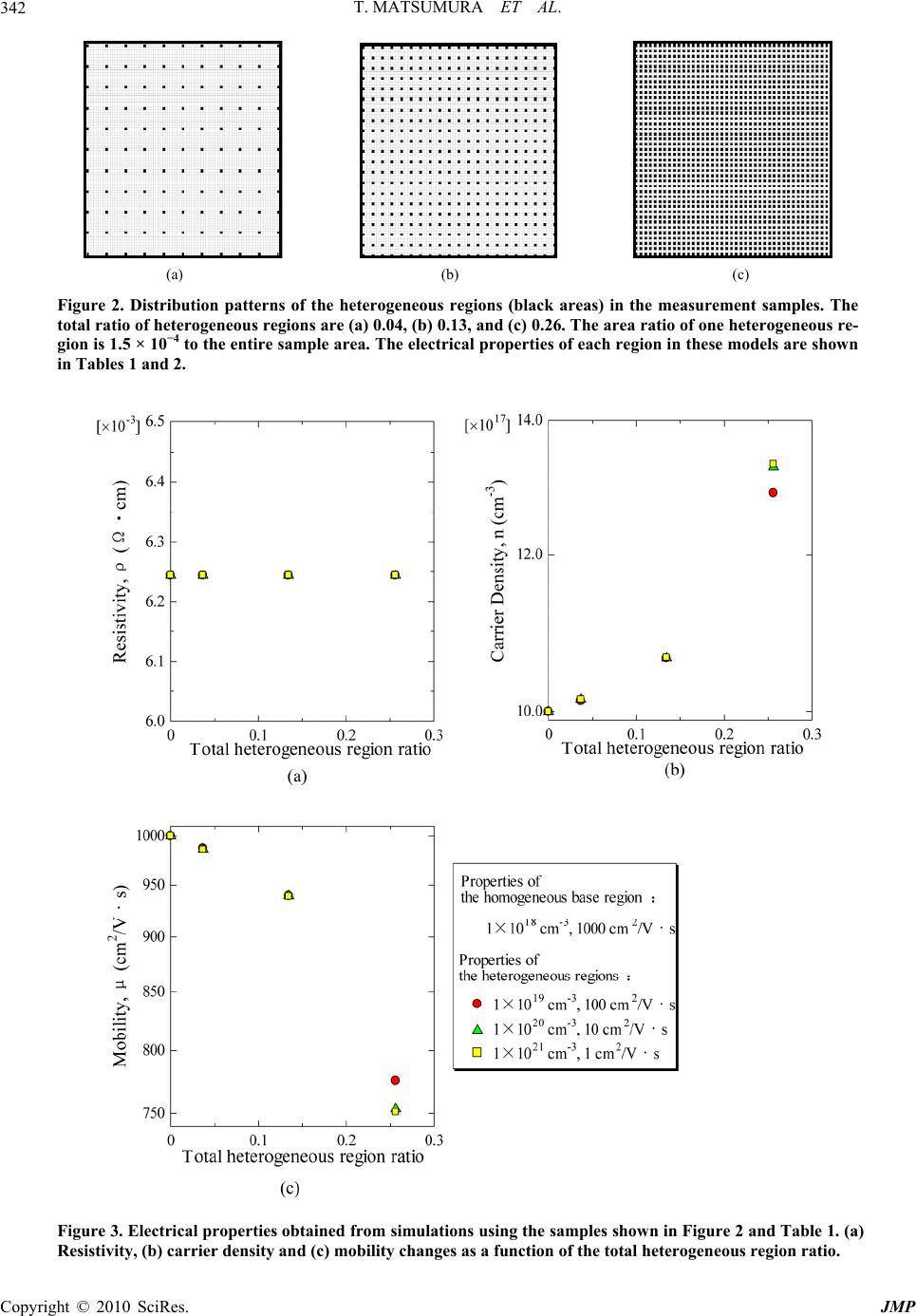 T. MATSUMURA ET AL. Copyright © 2010 SciRes. JMP 342 (a) (b) (c) Figure 2. Distribution patterns of the heterogeneous regions (black areas) in the measurement samples. The total ratio of heterogeneous regions are (a) 0.04, (b) 0.13, and (c) 0.26. The area ratio of one heterogeneous re- gion is 1.5 × 10⁻⁴ to the entire sample area. The electrical properties of each region in these models are shown in Tables 1 and 2. Figure 3. Electrical properties obtained from simulations using the samples shown in Figure 2 and Table 1. (a) Resistivity, (b) carrier density and (c) mobility changes as a function of the total heterogeneous region ratio.  T. MATSUMURA ET AL. Copyright © 2010 SciRes. JMP 343 Table 1. Electrical properties of the homogeneous base re- gion and heterogeneous regions in the inhomogeneous sam- ples shown in Figure 2. Carrier density (cm−3) Mobility (cm2/V·s) Resistivity (Ω·cm) Homogeneous base region 1 × 10¹⁸ 1000 6.24 × 10⁻³ Heterogeneous regions 1 × 10¹⁹~1021 1~100 6.24 × 10⁻³ and mobilities obtained by simulation showed large variations that were dependent upon the total heteroge- neous region ratios, as shown in Figures 3(b) and (c). The calculated carrier density increased with the increase in the heterogeneous region. The degree of change was almost the same, regardless of the carrier density of the heterogeneous region, although the increase in the calcu- lated carrier density was slightly larger when the carrier density of the heterogeneous region was high. The cal- culated mobility decreased with the increase in the het- erogeneous region. The degree of change was almost the same, regardless of the mobility of the heterogeneous region, although the degree of decrease was slightly large when the mobility of the heterogeneous region was low. From the results shown in Figures 3(b) and (c), devia- tions of the electrical properties of the inhomogeneous samples from those of the homogeneous base region were evaluated to be within several percent when the total ratio of the heterogeneous region was smaller than approximately 10%; therefore, the influence of inter- mixing of heterogeneous regions was not so large. How- ever, the deviations of the electrical properties from those of the homogeneous base region became signifi- cantly larger when the total ratio of the heterogeneous region was much larger than 10%. Heterogeneous regions that have more varied electri- cal properties and different resistivities from the homo- geneous base region were then intermixed in a different base sample. The electrical properties of the homogene- ous base region and heterogeneous regions used in these simulations are shown in Table 2. The distribution pat- terns of the heterogeneous regions were the same as the previous simulations. The calculated resistivities were changed by the intermixing, as shown in Figure 4(a). That is, the resistivities increased with increasing total ratio of the heterogeneous region when the resistivity of the heterogeneous region was higher than that of the homogeneous base region, while the resistivities de- creased when its resistivity was lower than that of the base region. The calculated carrier density and mobility also largely changed by intermixing of heterogeneous regions that had various carrier densities and mobilities, as shown in Figures 4(b) and (c). The degree of change in the calculated carrier densities tended to be large when the mobilities of the heterogeneous regions were high. Similarly, the degree of change in the calculated mobili- ties tended to be large when the carrier densities of the heterogeneous regions were high. In the above simulations, the heterogeneous regions were distributed over the entire sample area. The changes in the calculated electrical properties observed by the intermixing of heterogeneous regions were the expected ones. On the other hand, different changes were observed when the heterogeneous regions were concentrated lo- cally in the samples. The distribution patterns of the het- erogeneous regions are shown in Figures 5(a) and (b). The size of one heterogeneous region is the same as that used in the previous simulation models. The electrical properties examined in this simulation are shown in Ta- ble 3. The calculated resistivity and carrier density in these models changed similarly to those in the previous simulations in which the heterogeneous regions were dispersed over the entire sample area. That is, the changes were simply dependent upon the properties of the heterogeneous regions. However, the mobilities calculated in this case re- vealed a different change. The calculated mobilities for the samples with locally concentrated heterogeneous regions are shown in Figure 6. The calculated mobilities became larger than that of the homogeneous base mate- rial within a range of the total ratio of the heterogeneous region, although the mobility of the heterogeneous re- gion was definitely not higher than that of the homoge- neous base region. It is reasonable to expect that mobility will decrease with an increase of intermixing of hetero- Table 2. Electrical properties of the homogeneous base re- gion and heterogeneous regions in the inhomogeneous sam- ples shown in Figure 2. Carrier density (cm−3) Mobility (cm2/V·s) Resistivity (Ω·cm) Homogeneous base region 1 × 10¹⁹ 100 6.24 × 10⁻³ Heterogeneous regions 1 × 10¹⁷~1021 10~1000 6.24 × 10⁻⁵~10−1 Table 3. Electrical properties of the homogeneous base re- gion and heterogeneous regions in the inhomogeneous sam- ples shown in Figure 5. Carrier density (cm−3) Mobility (cm2/V·s) Resistivity (Ω·cm) Homogeneous base region 1 × 10¹⁹ 100 6.24 × 10⁻³ Heterogeneous regions 1 × 10²⁰, 1021 100 6.24 × 10⁻⁴, 10−5 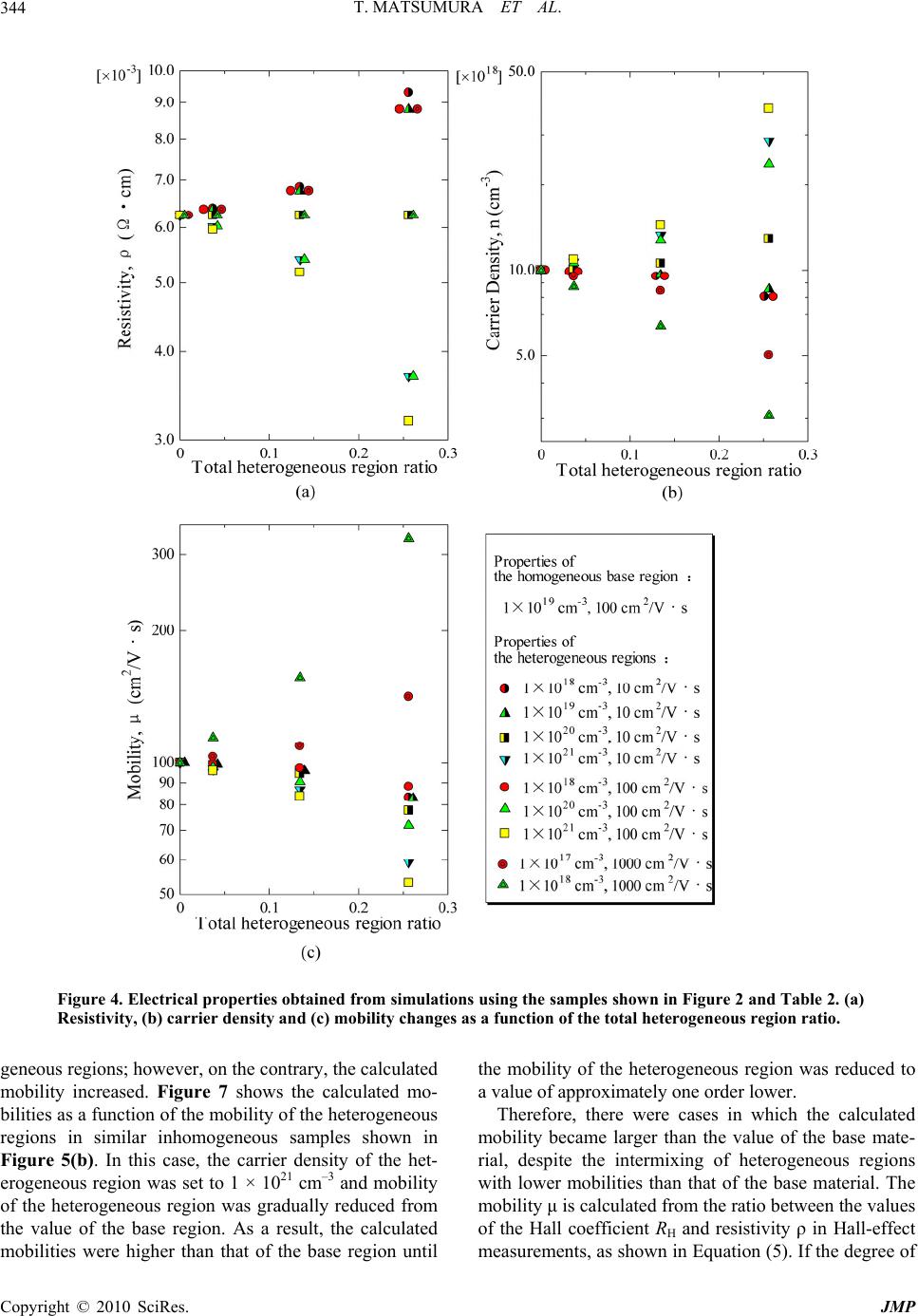 T. MATSUMURA ET AL. Copyright © 2010 SciRes. JMP 344 Figure 4. Electrical properties obtained from simulations using the samples shown in Figure 2 and Table 2. (a) Resistivity, (b) carrier density and (c) mobility changes as a function of the total heterogeneous region ratio. geneous regions; however, on the contrary, the calculated mobility increased. Figure 7 shows the calculated mo- bilities as a function of the mobility of the heterogeneous regions in similar inhomogeneous samples shown in Figure 5(b). In this case, the carrier density of the het- erogeneous region was set to 1 × 1021 cm–3 and mobility of the heterogeneous region was gradually reduced from the value of the base region. As a result, the calculated mobilities were higher than that of the base region until the mobility of the heterogeneous region was reduced to a value of approximately one order lower. Therefore, there were cases in which the calculated mobility became larger than the value of the base mate- rial, despite the intermixing of heterogeneous regions with lower mobilities than that of the base material. The mobility μ is calculated from the ratio between the values of the Hall coefficient RH and resistivity ρ in Hall-effect measurements, as shown in Equation (5). If the degree of 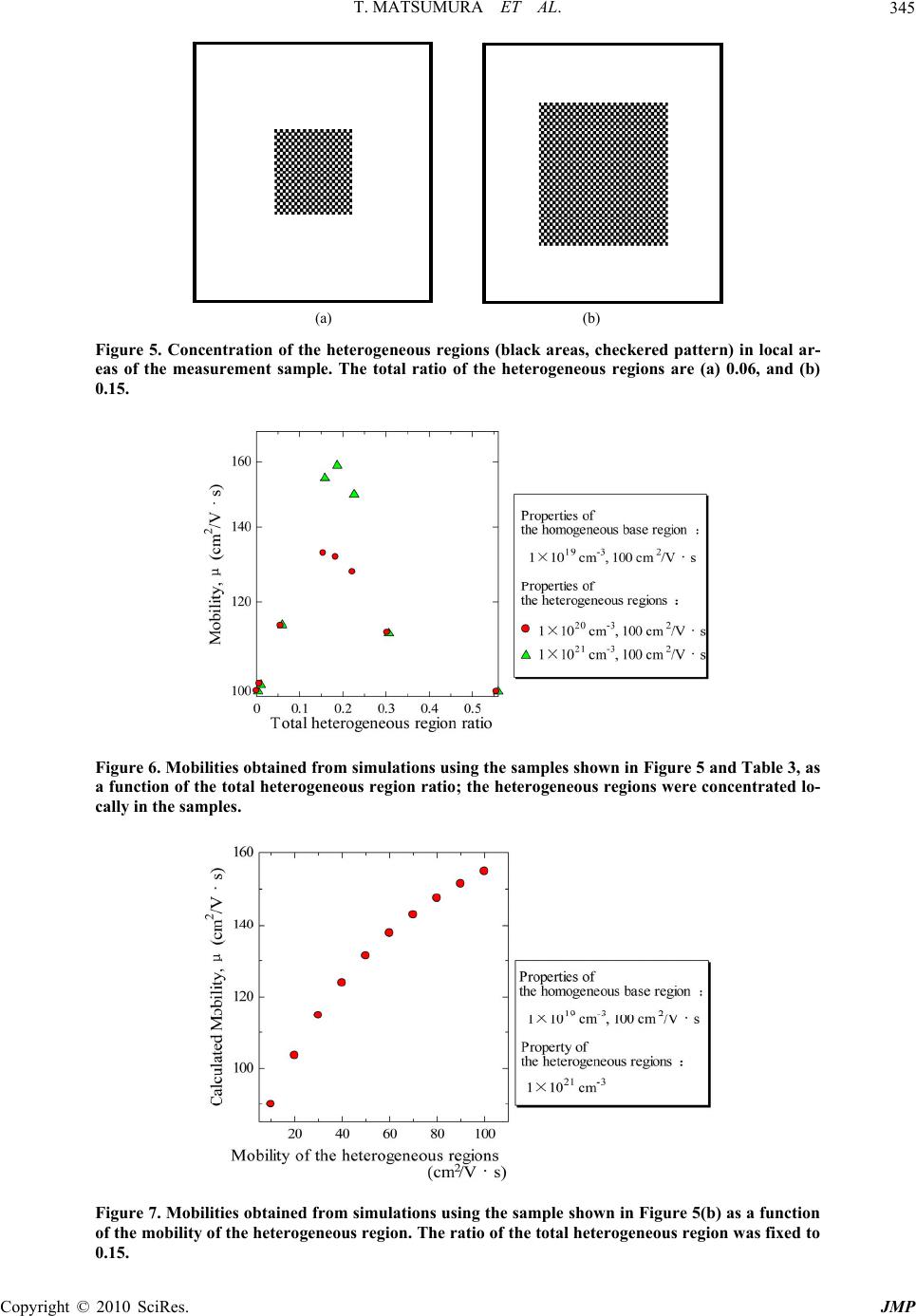 T. MATSUMURA ET AL. Copyright © 2010 SciRes. JMP 345 (a) (b) Figure 5. Concentration of the heterogeneous regions (black areas, checkered pattern) in local ar- eas of the measurement sample. The total ratio of the heterogeneous regions are (a) 0.06, and (b) 0.15. Figure 6. Mobilities obtained from simulations using the samples shown in Figure 5 and Table 3, as a function of the total heterogeneous region ratio; the heterogeneous regions were concentrated lo- cally in the samples. Figure 7. Mobilities obtained from simulations using the sample shown in Figure 5(b) as a function of the mobility of the heterogeneous region. The ratio of the total heterogeneous region was fixed to 0.15.  T. MATSUMURA ET AL. Copyright © 2010 SciRes. JMP 346 Figure 8. Changes in the resistivity ρ and Hall coefficient RH obtained from the simulations using the samples shown in Figure 5(b) as a function of the mobility of the heterogeneous regions. (a) (b) Figure 9. Typical examples of the calculated electrical potential distributions on the resistivity (left sides) and Hall effect (right sides) measurements of the (a) homogeneous and (b) inhomogeneous samples in which heterogeneous regions were locally concentrated. The carrier density and mobil- ity of the homogeneous base region were 1 × 1019 cm−3 and 100 cm2/V·s, respectively, while those of the heterogeneous regions were 1 × 1020 cm−3 and 100 cm2/V·s.  T. MATSUMURA ET AL. Copyright © 2010 SciRes. JMP 347 variation of the Hall coefficient and resistivity by inter- mixing of heterogeneous regions are not same, then the value of mobility calculated from the ratios will fluctuate depending upon the ratios. The degree of change (de- crease) in resistivity by intermixing of heterogeneous regions is larger than the degree of change (decrease) in the Hall coefficient in this case, as shown in Figure 8. Therefore, mobilities calculated from the ratio become larger than that of the base material. We have simulated about more various inhomogene- ous samples and confirmed that samples in which het- erogeneous regions locally concentrated showed the similar tendencies described above. Typical electrical potential distributions in such sample are shown in Fig- ure 9 with those of a homogeneous sample. The poten- tial distribution is markedly distorted in the locally het- erogeneous region concentrated sample. The measured voltage between the terminals C and D in the resistivity measurement (left sides) become considerably small when the resistivities of the heterogeneous regions are smaller than that of the homogeneous base region. On the other hand, the Hall voltages between the terminals A and C in the Hall effect measurement (right sides) are almost same about the both samples. Therefore, the value of the mobility calculated from the values of Hall coeffi- cient and resistivity become larger than that of the ho- mogeneous sample. 4. Conclusions The effect of intermixing of heterogeneous regions in compound semiconductor thin films on the electrical properties obtained by the van der Pauw method were investigated by simulation using the FEM. The calcu- lated electrical properties varied predictably according to the electrical properties of the heterogeneous regions when the regions were dispersed over the entire sample area. The deviations of electrical properties of inhomo- geneous samples from those of the homogeneous base materials were not very large when the total ratio of the heterogeneous region was lower than approximately 10% in such cases. On the other hand, the calculated mobility tended to increase unexpectedly by the intermixing of heterogeneous regions when the regions were concen- trated locally in the samples, even though the mobilities of the intermixed heterogeneous regions were lower than that of the base material. Thus, the electrical properties of inhomogeneous compound semiconductor thin films obtained by the van der Pauw method are dependent upon the distribution patterns of the heterogeneous re- gions, and unexpected values may be obtained in cases in which the heterogeneous regions are concentrated locally in the measurement samples. 5. References [1] L. J. van der Pauw, “A Method of Measuring Specific Resistivity and Hall Effect of Discs of Arbitrary Shape,” Philips Research Reports, Vol. 13, February 1958, pp. 1-9. [2] H. Komaki, T. Nakamura. R. Katayama, K. Onabe, M. Ozeki and T. Ikari, “Growth of In-Rich InGaN Films on Sapphire via GaN Layer By RF-MBE,” Journal of Crys- tal Growth, Vol. 301-302, April 2007, pp. 473-477. [3] T. Yamaguchi and Y. Nanishi, “Indium Droplet Elimina- tion by Radical Beam Irradiation for Reproducible and High-Quality Growth of InN by RF Molecular Beam Epi- taxy,” Applied Physics Express, Vol. 2, No. 5, April 2009, p. 051001. [4] B. N. Pantha, J. Li, J. Y. Lin and H. X. Jiang, “Evolution of Phase Separation in In-Rich InGaN Alloys,” Applied Physics Letters, Vol. 96, No. 23, June 2010, p. 232105. [5] A. Krtschil, A. Dadgar, N. Oleynik, J. Blasing, A. Diez and A. Krost, “Local P-Type Conductivity in Zinc Oxide Dual-Doped with Nitrogen and Arsenic,” Applied Physics Letters, Vol. 87, No. 26, December 2005, p. 262105. [6] D. W. Koon, “Effect of Contact Size and Placement, and of Resistive Inhomogeneities on van der Pauw Measure- ments,” Review of Scientific Instruments, Vol. 60, No. 2, February 1989, pp. 271-274. [7] D. W. Koon and C. J. Knickerbocker, “What do You Measure When You Measure the Hall Effect?” Review of Scientific Instruments, Vol. 64, No. 2, February 1993, pp. 510-513. [8] D. W. Koon and C. J. Knickerbocker, “Effects of Macro- scopic Inhomogeneities on Resistive and Hall Measure- ments on Crosses, Cloverleafs, and Bars,” Review of Sci- entific Instruments, Vol. 67, No. 12, December 1996, pp. 4282-4285. [9] D. W. Koon, “Nonlinearity of Resistive Impurity Effects on van der Pauw Measurements,” Review of Scientific In- struments, Vol. 77, No. 9, September 2006, p. 094703. [10] O. Bierwagen, T. Ive, C. G. Van de Walle and J. S. Speck, “Causes of Incorrect Carrier-Type Identification in van der Pauw-Hall Measurements,” Applied Physics Letters, Vol. 93, No. 24, December 2008, p. 242108. [11] N. Yom-Tov, C. Saguy, A. Bolker, R. Kalish and Y. E. Yaish, “Accurate Carrier-Type Determination of Non- homogeneously Doped Diamond,” Journal of Applied Physics, Vol. 108, No. 4, August 2010, p. 043711. |