Circuits and Systems
Vol. 3 No. 2 (2012) , Article ID: 18533 , 10 pages DOI:10.4236/cs.2012.32018
An Analytical Approach for Fast Automatic Sizing of Narrow-Band RF CMOS LNAs*
Electronic & Electrical Engineering Department, Hongik University, Jochiwon, South Korea
Email: jychoi@hongik.ac.kr
Received November 25, 2011; revised December 26, 2011; accepted January 4, 2012
Keywords: Automatic Synthesis; Analytical Approach; CMOS LNA; Narrow Band; Cascode
ABSTRACT
We introduce a fast automatic sizing algorithm for a single-ended narrow-band CMOS cascode LNA adopting an inductive source degeneration based on an analytical approach without any optimization procedure. Analytical expressions for principle parameters are derived based on an ac equivalent circuit. Based on the analytical expressions and the power-constrained noise optimization criteria, the automatic sizing algorithm is developed. The algorithm is coded using Matlab, which is shown capable of providing a set of design variable values within seconds. One-time Spectre simulations assuming usage of a commercial 90 nm CMOS process are performed to confirm that the algorithm can provide the aimed first-cut design with a reasonable accuracy for the frequency ranging up to 5 GHz. This work shows one way how accurate automatic synthesis can be done in an analytical approach.
1. Introduction
In the field of RF transceiver design, there is a strong demand to digitalize even RF analog parts to mount a transceiver on a single chip [1,2] to utilize the capability of automatic synthesis in digital circuit design. However, the low noise amplifier (LNA), which is a critical building block in any RF front-end, is not ready for digitalization yet. Many efforts have been done for design automation of LNA beforehand since the design of LNA is a time-consuming task that typically relies heavily on the experience of RF designers. LNA design automation can significantly simplify the design task, and also opens a possibility towards digitalization.
There are two basic methods for LNA design automation: simulation based or equation based. Although the simulation-based methods [3,4] are more accurate, they are time consuming due to optimization procedures. On the other hand, equation-based methods [5-7] are faster, but are dependent on the accuracy of the models used. To overcome the disadvantages in some extent, advanced methods using both of equation-based and simulationbased approaches [8-10] have been also suggested.
The difficulties in design automation of LNA lie in several aspects. It is topology dependent, and the design itself is difficult involving trade-offs among critical figures of merits such as NF, power gain, impedance matching, power consumption, linearity, and stability. Mentioning the difficulties in a manual design, for example, even only for input and output matching, many iteration steps are needed. It should be also redesigned every time when the fabrication process is changed. Therefore it is desirable if the first-cut design synthesis can be done automatically and fast with an acceptable accuracy.
The purpose of this work is to suggest a methodology for providing a set of first-cut design variables for a narrow-band LNA with a reasonable accuracy once design and process specifications are given.
We introduce a speedy automatic sizing algorithm for a single-ended narrow-band cascode LNA adopting inductive source degeneration based on an analytical approach without any optimization procedure. In Section 2, design assumptions are discussed. In Section 3, analytical expressions for principle parameters are derived based on an ac equivalent circuit assuming a resistive output termination. In Section 4, the developed automatic sizing algorithm is explained in detail. In Section 5, verifications are given to check the accuracy of the automatic sizing results.
2. Design Assumptions
There are many topologies for narrow-band LNAs, however, typical topologies include cascode, common source, and differential configurations, and the cascode structure with an inductive source degeneration shown in Figure 1 is the most attractive one in single-ended topologies since it gives smaller input capacitance and larger in-out isolation [11]. In this work, the cascode LNA topology shown in Figure 1 is chosen as the objective circuit for automatic sizing even though the same approach can be applied to the other topologies.
There are several assumptions made in this work as follows:
1) Narrow-band LC matching networks are used for input and output as shown in Figure 1. R1 is used to provide capability for adjusting power gain. As the output termination, two cases are considered: resistive or capacitive termination.
2) For sizing of the MOS transistors M1 and M2, the power-constrained noise optimization (PCNO) criteria [11] is adopted to trade off noise performance against power consumption.
3) Ideal inductors and capacitors are used by assuming usage of off-chip components. The series resistances of the on-chip inductors can be considered as well, but we choose a simpler case.
4) A current-mirror biasing is adopted as shown in Figure 1.
5) The widths of M1 and M2 are set as same.
6) The design specifications include operating frequency, input and output terminations, power consumption, power gain, and sufficiently low input and output reflection coefficients S11 and S22.
7) The design variables include Lg, Ls, L1, Ci, Co, R1, RDB, and RB including the widths of M1, M2, and MB in Figure 1.
3. Derivation of Analytic Expressions for Principal Parameters
3.1. Input Impedance
Figure 2 is the whole ac equivalent circuit for the cascode LNA shown in Figure 1 including the input signal source and the output resistive termination. We note that, compared to the complete equivalent circuit of the BSIM4 NMOS transistor in SPICE, only the back-gate transconductance gmb and the gate-body capacitance Cgb in the transistor model are ignored to simplify the analysis. The distributed resistances including Rs, Rd, Rg, and Rsub, which are included in the BSIM 4 transistor model, are also ignored since they are negligible in large transistors.
In Figure 2, gm1 and gm2 denote the transconductances of M1 and M2, respectively. Cgs, Cgd, and Cds denote the gate-source, gate-drain, and drain-source capacitances of the NMOS transistors, respectively. Cjs and Cjd denote the source-body and drain-body junction capacitances, and CL is equal to the sum of Cdg2 and Cjd2, which are the
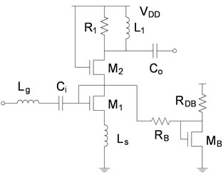
Figure 1. Assumed cascode LNA circuit.
capacitances present at the drain node of M2 in Figure 1.
The impedances Zin, Zin1, Zin2, Zo, Zout, Zout1, and Zout2 are self-defined in the circuit. We first consider the resistive output termination case and discuss the capacitive output termination case later in Section 6. We note that Cgs, Cgd, and Cds are replaced by Csg, Cdg, and Csd, respectively, in some part of our derivations for input and output impedances considering the non-reciprocal nature of gate-oxide capacitances in the BSIM4 MOSFET capacitance model [12].
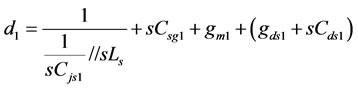
First, we derive Zin by deriving Zo, Zin2, and Zin1 in order. We note that, we use s and jω without differentiation since we are dealing with ac response only.
To derive Zo at the operating frequency, the series Co and Rso in Figure 2 can be transformed to the parallel equivalents, Cp and Rp [11]. Then Yo = 1/Zo is simply expressed as
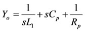 , (1)
, (1)
where Rp = Rso(Q2 + 1), Cp = CoQ2/(Q2 + 1), and Q = 1/(ωRsoCo).
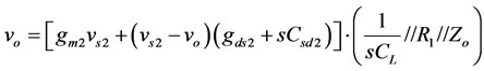
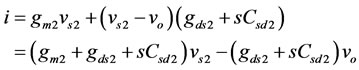
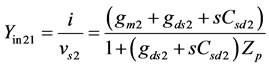
Figure 3 shows the ac equivalent circuit to derive an expression for Zin2. Notice that, in the circuit shown in Figure 3, the non-reciprocal capacitance Csd2 is used instead of Cds2, since we are looking into the source of M2.
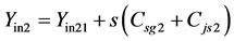
By neglecting the parallel (Csg2 + Cjs2) branch, we derive the input admittance Yin21 first, and add s(Csg2 + Cjs2) to find Yin2 = 1/Zin2. When the (Csg2 + Cjs2) branch is neglected, the circuit can be characterized by (2) and (3).
 (2)
(2)
 (3)
(3)
By eliminating vo in (2) and (3), we can express Yin21 as
 , (4)
, (4)
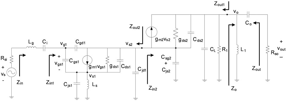
where Zp = (1/sCL)//R1//Zo.
Then Yin2 are expressed as
 . (5)
. (5)
Figure 4 shows the ac equivalent circuit to derive an expression for Zin1. The circuit can be characterized by (6), (7), and (8).
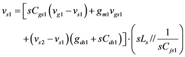 (6)
(6)
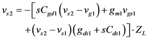 (7)
(7)
 , (8)
, (8)
where ZL = (1/(sCjd1))//Zin2.
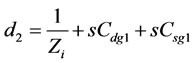
By eliminating vs1 and vs2 in (6), (7) and (8), Yin1 = 1/Zin1 is expressed as
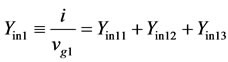 , (9)
, (9)
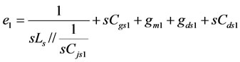
where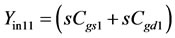 ,
,
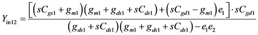 ,
,
 ,
,
and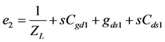 .
.
Then Zin is expressed as
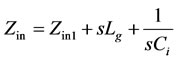 . (10)
3.2. Output Impedance
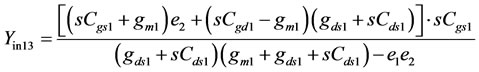
Zout derivation can be done similarly as the Zin derivation using the equivalent circuit in Figure 2 assuming Rsi input termination. We present the results only here.
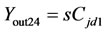
Yout2 = 1/Zout2 is expressed as
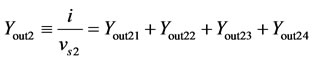 , (11)
where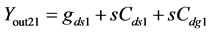 ,
,
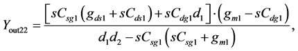
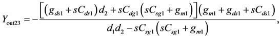
Figure 3. AC equivalent circuit to find Zin2.
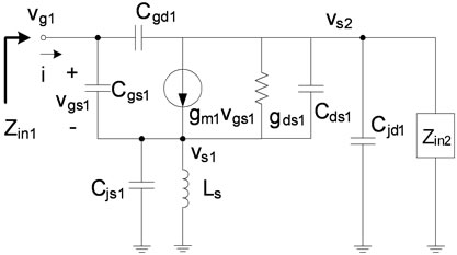
Figure 4. AC equivalent circuit to find Zin1.
 ,
,
 ,
,
 and
and 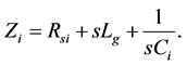
Yout1 = 1/Zout1 is expressed as
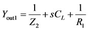 , (12)
where 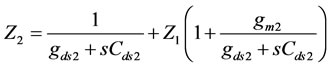 and
and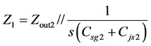 .
.
Then Zout is expressed as
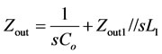 . (13)
3.3. Power Gain
To derive the LNA voltage gain, the equivalent circuit in Figure 2 is simplified into the one shown in Figure 5,
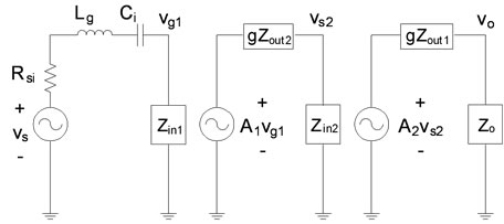
Figure 5. Equivalent circuit to find the voltage gain.
where the whole circuit is expressed as a 3-stage cascaded amplifier.
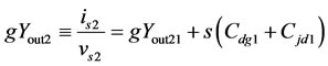
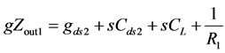
Zin1, Zin2 and Zo in Figure 5 are already derived in (9), (5) and (1), respectively. Notice that A1vg1, gZout2, A2vs2, and gZout1 are the Thevenin equivalent voltages and impedances of the 2nd and 3rd gain stages in Figure 2. Therefore gZout2 and gZout1 differ from Zout2 and Zout1 in (11) and (12), respectively, and can be derived as follows.
By definition, gZout2 corresponds to the impedance seen to the left of the vs2 node when vg1 = 0 in Figure 2, and can be derived using the equivalent circuit shown in Figure 6.
The circuit can be characterized by the Equations (14) and (15).
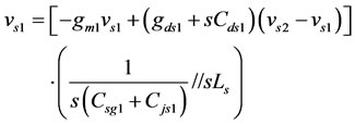 (14)
(14)
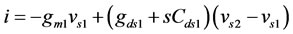 (15)
(15)
By eliminating vs1 in (14) and (15), gYout21 is expressed as
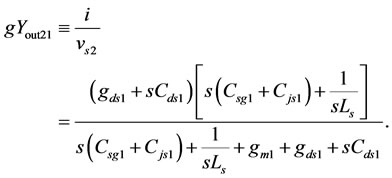 (16)
(16)
Then gYout2 =1/gZout2 is expressed as
 . (17)
By definition, A1 corresponds to the voltage gain vs2o/vg1, where vs2o is the vs2 node voltage when open, and can be derived using the equivalent circuit shown in Figure 7. The circuit can be characterized by the Equations (18) and (19).
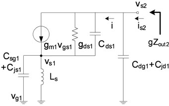
Figure 6. AC equivalent circuit to find gZout2.
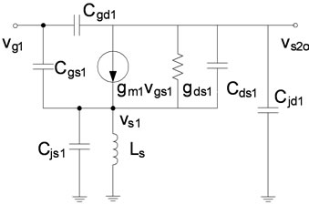
Figure 7. AC equivalent circuit to find A1.
 (18)
(18)
 (19)
(19)
By eliminating vs1 in (18) and (19), we get
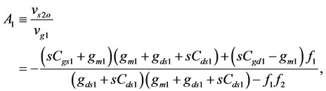 (20)
(20)
where 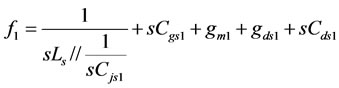 and
and
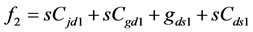 .
.
gZout1 corresponds to the impedance seen to the left of the vo node with vs2 = 0 in Figure 2. Since gm2vs2 and (Cgs2 + Cjs2) do not function when vs2 = 0, gYout1 = 1/gZout1 is simply expressed as
 . (21)
A2 corresponds to the voltage gain voo/vs2, where voo is the vo node voltage when open, and A2 derivation can be done in the similar fashion to the one for A1 derivation. The resulting A2 is expressed as
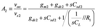 . (22)
In Figure 2, the available input power Pi, which is supplied to the LNA when impedance matched, is defined as
 . (23)
The maximum output power Po, which is supplied to the resistive load Rso when impedance matched, is expressed as
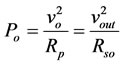 , (24)
where vo and vout are defined in Figure 2, and Rp is the transformed parallel resistance of Rso, which is already defined relating (1).
Then the available power gain G is expressed as
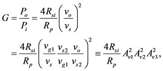 (25)
(25)
where Av1, Av2, and Av3 can be easily derived from Figure 5 as follows.
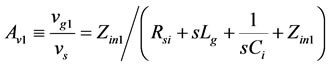 (26)
(26)
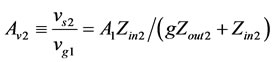 (27)
(27)
 (28)
(28)
4. Automatic Sizing Algorithm
Figure 8 shows the automatic sizing algorithm developed in this work. The inputs to the algorithm include design and process specifications, and the outputs include synthesized design variable values are for RDB, W, nfb, Ls, Lg, Ci, R1, L1, Co. Here, we explain the procedures from top to bottom in accordance with each step, which is explicitly indicated in Figure 8.
4.1. 1st Step: Entering Design and Process Specifications
The 1st step in the automatic sizing is to enter the design
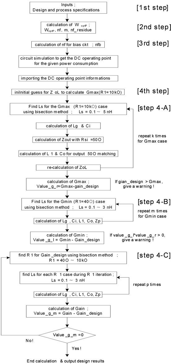
Figure 8. Automatic sizing algorithm.
and process specifications. The design specifications include the operating frequency f, the input output terminations Rsi and Rso, the supply current IDD, the desired power gain Gain_design. Instead of IDD, the power consumption PWR and the supply voltage VDD can be entered to calculate IDD by PWR/VDD. The process specifications include the transistor channel length L, the transistor channel width per finger WF, and the maximum finger number nf_max defined for one unit of transistors.
4.2. 2nd Step: Calculation of Optimum Transistor Width
The next step is to calculate the transistor channel width W for optimum noise performance. The width for optimum noise performance is usually too large for practical use, and therefore the power-constrained noise optimization (PCNO) device width WoptP [11] is adopted as W in this work. WoptP is calculated according to the last rough equation in (29).
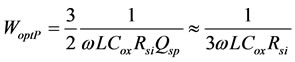 (29)
(29)
As shown in (29), WoptP increases continuously as the frequency decreases. Therefore it may be necessary to define a maximum value for W considering lower frequency design. We suggest to limit W below 1000 μm.
If WF and nf_max are defined, the finger number nf is first calculated as W/WF, and the number of the maximum-fingered units m is calculated as the integer value of nf/nf_max, and the residual finger number nf_residue is determined as the residue to give an information for the transistor layout. Then the final W is determined by W = WF × (m × nf_max + nf_residue). We note that WF and nf_max are usually defined in most of recent processes.
4.3. 3rd Step: Calculation of Bias Circuit Design Variables and Getting DC Operating Point Information
The next step is to determine the bias circuit variable values and to get the dc operating point information.
The finger number for the bias transistor nfb and the drain bias resistance RDB in Figure 1 should be determined. By limiting the bias circuit current around 100 μA, for example, we can determine nfb by nfb = (100 μA/IDD) × nf. For the decoupling resistor RB, we can simply use 5 kΩ, which is a reasonable value.
The next procedure is to determine RDB, which, however, is very difficult to determine by calculation. Since IDD is sensitive to the value of RDB, it should be manually determined to give the specified IDD value by dc circuit simulations. This procedure is one obstacle against full design automation in this work. However, it is an essential procedure since it provides the accurate operating point information to proceed with the remaining part of the design automation. The needed operating point information include the values of gm, gds, Cgs, Csg, Cgd, Cdg, Cds, Csd, Cjs, and Cjd of M1 and M2 in Figure 1, which should be imported into the automatic sizing algorithm.
4.4. 4th Step: Iterations to Determine Design Variable Values
There are three main iteration loops in the automatic sizing algorithm as shown in Figure 8. The 1st loop finds Gmax, which corresponds to the case with the upper limit of R1, which is chosen arbitrarily large enough as 10 kΩ in this work. To find Gmax, we need to find all the design variable values for the Gmax case simultaneously. Iteration is needed since the input and output matching designs affect each other. The 2nd loop finds Gmin, which corresponds to the case with the lower limit of R1, which is arbitrarily chosen small as 40 Ω in this work to allow a larger allowable gain range. This iteration is also needed for the same reason explained for the Gmax case. The 3rd loop finds the proper R1 value for the desired gain Gain_ design by the bisection method, which lies within the lower and upper boundaries Gmin and Gmax, and its inner loop finds the corresponding design variable values for the present gain value during iteration similarly as in the 1st and 2nd iteration loops.
4.4.1. Iterations to Solve for the Gmax Case
As explained above, Zin1 is affected by output matching design, and Zout is affected by input matching design. Therefore we need some iteration to determine Ls. Since Zin2 is affected by Zo, which is unknown yet, we need an initial guess for Zo to find the 1st Ls value. As shown in Figure 8, an initial guess for ZoL = Zo//(1/sCL) is given as 50/g·m2, which is shown to be large enough for all possible situations in the procedure, to solve for Zin2 by (5).
The impedance seen at the gate of M1 is equal to Zin1, which is derived in (9). By setting the real part of Zin1 Re(Zin1) equal to Rsi for input impedance matching, we can find Ls. However this equation Re(Zin1) = Rsi is too complicated to get the solution directly with the other present design variables values given, and therefore Ls is solicited numerically within the lower and upper boundaries of 0.1 nH and 5 nH. We use the bisection method for this purpose.
The next procedure is to calculate Lg and Ci, which nullify the imaginary part of Zin1 Im(Zin1) in Figure 2. Zin1 is usually capacitive to give a negative value for Im(Zin1), and therefore Lg can be calculated using the equation Im(Zin1) – 1/(ωCi) + ωLg = 0, where Ci is simply a large dc blocking capacitor. We first calculate Lg1, which nullifies Im(Zin1) using Im(Zin1) + ωLg1 = 0. Although Ci is larger the better, considering the layout size, 1/(ωCi) = ωLg1/10 is used to determine Ci. Lg is then recalculated using Im(Zin1) – 1/(ωCi) + ωLg = 0.
Depending on to the operating frequency and the desired gain, Zin1 may happen to be inductive, or this situation can happen in the middle of the iterations. For this case, a nominal single bond wire inductance of 1 nH is assumed for Lg and Im(Zin1) – 1/ωCi + ωLg = 0 is used to calculate the required Ci value.
In the next procedure, the design variables L1 and Co are determined using the equations Re(Zout) = Rso and Im(Zout) = 0 for output impedance matching to Rso, where Re(Zout) is the real part of Zout expressed in (13).
If we let Zout1 in (12) equal to A + jB, the real and imaginary parts of Zout1//jωL1 in (13) are expressed as
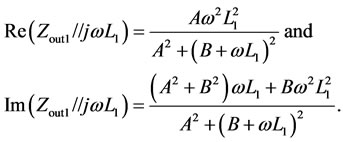 (30)
(30)
Then by letting Re(Zout) = Re(Zout1//jωL1) = Rso, L1 is expressed as
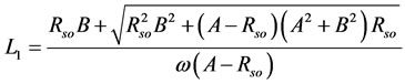 (31)
(31)
By letting Im(Zout) = Im(Zout1//jωL1) – 1/(ωCo) = 0, Co is expressed as
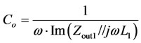 . (32)
Using (31) and (32), L1 and Co can be simply calculated.
Now the 1st set of the design variable values are ready to update ZoL and the remaining iterations are performed to find the final design variable values for the Gmax case. It was found that the iteration number for this loop should be larger than 10.
Right after the iteration loop, A1, gZout2, A2, and gZout1 are calculated using (20), (17), (22), and (21), respectively, and Gmax is calculated using (25).
If the Gmax value is smaller than the desired gain, the routine gives a warning and stops.
4.4.2. Iterations to Solve for the Gmin Case
The 2nd loop finds the design variable values for the Gmin case. The same iteration as above with the last ZoL value as an initial guess is performed to find Gmin using (25) again.
4.4.3. Iterations to Solve for the Gain_Design Case
The 3rd loop finds the proper R1 value for the desired gain Gain_design using the bisection method while the inner loop finds the corresponding design variable values for the present gain value. This inner iteration loop is exactly same as the 1st and 2nd loops. After all the design variables are determined for the present gain value, the gain is calculated using (25) again. If the calculated gain is equal to Gain_design within the allowed tolerance, the calculation stops to output the final set of the design variable values, which include W, nf, m, nf_residue, nfb, Ls, Lg, Ci, R1, L1, and Co.
5. Verifications
The automatic sizing algorithm explained in Section 4 was coded using Matlab (Version 7.9.0.529) assuming usage of a 90 nm commercial CMOS process. The design variable sets for seven different operating frequencies ranging from 0.7 GHz to 5 GHz were synthesized, and verifications were done by one-time Spectre circuit simulations with the corresponding BSIM4.5.0 MOSFET model [12] for the assumed process.
The design specifications include ID = 5 mA, VDD = 1.2 V, Gain_design = 21 dB, and Rsi = Rso = 50 Ω. The process specifications include L = 75 nm, WF = 3 μm, and nf_max = 64, where 75 nm for L is the effective channel length in this process. The maximum transistor width was set as Wmax = nf_max × m × WF = 64 × 5 × 3 μm = 960 μm, which is below 1000 μm as we suggested.
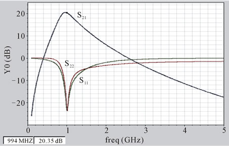
As examples of the verifications, Figures 9 and 10 show the simulated LNA characteristics without any tuning for the operating frequency of 1 GHz and 5 GHz, respectively, when the corresponding sets of the design variable values obtained using the automatic sizing algorithm are used for the simulations. The synthesized design variable values are as follows;
For 1 GHz design, RDB = 12.7 kΩ, W = 960 μm (m = 5, nf_residue = 0), nfb = 6, Ls = 1.382 nH, Lg = 19.557 nH, Ci = 14.25 pF, R1 = 497.1 Ω, L1 = 11.904 nH, Co = 1.447 pF.
For 5 GHz design, RDB = 5.96 kΩ, W = 231 μm (m = 1, nf_residue = 13), nfb = 2, Ls = 0.5383 nH, Lg = 2.690 nH, Ci = 4.142 pF, R1 = 1.752 kΩ, L1 = 2.813 nH, Co = 0.190 pF.
Table 1 summarizes the simulated results of the seven designs, which reside in the frequency range, where the automatic sizing program could provide the design variable set for Gain_design of 21 dB. Notice that, for the operating frequencies below 1 GHz, the synthesized W values are restricted to below 960 μm, which is equal to the value for Wmax.
In Table 1, we can see that the input and output matchings (S11 and S22) are pretty good for all the designs, and the noise figure is pretty close to the noise figure minimum, which demonstrates the adequacy of the designs.
We note that power gain values are about the same with S21 values. The S21 values in Table 1 are smaller than the desired gain of 21 dB. This seems to be caused by neglecting gmb, Cgb, Rs, Rd, Rg, and Rsub in the equivalent circuit in Figure 2. However we believe that the result is pretty good for the first-cut quick design.
 (a)
(a)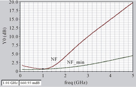 (b)
(b)
Figure 9. Simulated (a) s parameter and (b) noise characteristics for f = 1 GHz: S21 = 20.31 dB, NF = 0.660 dB, NFmin = 0.585, S11 = –23.6 dB, S22 = –23.0 dB.
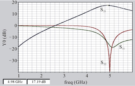
Figure 10. Simulated s parameters for f = 5 GHz: S21 = 17.16 dB, S11 = –16.9 dB, S22 = –34.8 dB.
Table 2 summarizes the synthesized available gain ranges with the corresponding R1 values for each design. We can see that a wide range of power gain can be obtained by varying the R1 values as expected.
6. Conclusions
The analytical expressions for the principle parameters
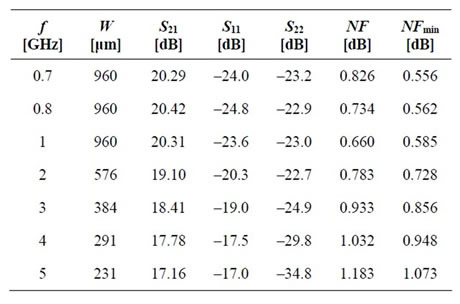
Table 1. Simulation summary for the desired gain Gain_ design of 21 dB.
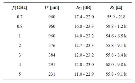
Table 2. Synthesis summary for the available gain ranges with the corresponding R1 values.
were derived using the ac equivalent circuit of the singleended narrow-band cascode CMOS LNA adopting the inductive source degeneration. Based on the expressions, the automatic sizing algorithm was developed by adopting the power-constrained noise optimization criteria. The algorithm was coded using Matlab, and could provide a set of design variable values within seconds. One-time Spectre simulations without any tuning assuming usage of a commercial 90 nm CMOS process were performed to confirm that the automatic sizing program can synthesize the aimed first-cut design with a reasonable accuracy for the frequency range reaching up to 5GHz.
This work showed in detail how the accurate automatic sizing can be done in an analytical approach. The approach can be applied to a common source LNA more easily since the derivation of principal parameters will be simpler with a fewer gain stages. It can be also applied to a differential LNA easily since the derivation will be basically same. The approach seems applicable to more complicated designs even though the derivation procedures will contain enhanced complexity.
The automatic sizing program may be utilized efficiently for additional tuning purpose. For example, after examining the first-cut synthesis result with verifying circuit simulations, a smaller value for WM2 compared to the synthesized one for WM1 can be entered into the automatic sizing program to obtain another design variable set for better linearity.
REFERENCES
- K. Muhammad, R. B. Staszewski and D. Leipold, “Digital RF Processing: Toward Low-Cost Reconfigurable Radios,” IEEE Communications Magazine, Vol. 43, No. 8, 2005, pp. 105-113. doi:10.1109/MCOM.2005.1497564
- A. A. Abidi, “The Path to the Software-Defined Radio Receiver,” IEEE Journal of Solid-State Circuits, Vol. 42, No. 5, 2007, pp. 954-966. doi:10.1109/JSSC.2007.894307
- G. Zhang, A. Dengi and L. R. Carley, “Automatic Synthesis of a 2.1 GHz SiGe Low Noise Amplifier,” Proceedings of IEEE Radio Frequency Integrated Circuits Symposium, Seattle, 2-4 June 2002, pp. 125-128.
- M. Chu and D. J. Allstot, “An Elitist Distributed Particle Swarm Algorithm for RFIC Optimization,” Proceedings of Asia and South Pacific Design Automation Conference, Shanghai, 18-21 January 2005, pp. 671-674.
- P. Vancorenland, C. De Ranter, M. Steyaert and G. Gielen, “Optimal RF Design Using Smart Evolutionary Algorithms,” Proceedings of Design Automation Conference, Los Angeles, 4-8 June 2000, pp. 7-10.
- G. Tulunay and S. Balkır, “A Compact Optimization Methodology for Single-Ended LNA,” Proceedings of IEEE International Symposium Circuits and Systems, Geneva, 23-26 May 2004, pp. V-273-V-276.
- T.-K. Nguyen, C.-H. Kim, G.-J. Ihm, M.-S. Yang and S.-G. Lee, “CMOS Low-Noise Amplifier Design Optimization Techniques,” IEEE Transactions on Microwave Theory and Technique, Vol. 52, No. 5, 2004, pp. 1433- 1442. doi:10.1109/TMTT.2004.827014
- G. Tulunay and S. Balkir, “Automatic Synthesis of CMOS RF Front-Ends,” Proceedings of IEEE International Symposium Circuits and Systems, Island of Kos, 21-24 May 2006, pp. 625- 628.
- A. Nieuwoudt, T. Ragheb and Y. Massoud, “SOC-NLNA: Synthesis and Optimization for Fully Integrated Narrow-Band CMOS Low Noise Amplifiers,” Proceedings of Design Automation Conference, San Francisco, 24-28 July 2006, pp. 879-884.
- W. Cheng, A. J. Annema and B. Nauta, “A Multi-Step PCell for LNA Design Automation,” Proceedings of IEEE International Symposium Circuits and Systems, Seattle, 18-21 May 2008, pp. 2550-2553.
- T. H. Lee, “The Design of CMOS Radio-Frequency Integrated Circuits,” 2nd Edition, Cambridge University Press, Cambridge, 2004.
- BSIM4.5.0 MOSFET Model, User’s Manual, University of California, Berkeley, 2004.
NOTES
*This work was supported by 2011 Hongik University Research Fund (sponsors).