Circuits and Systems
Vol. 3 No. 3 (2012) , Article ID: 20197 , 7 pages DOI:10.4236/cs.2012.33030
Optimization of the Voltage Doubler Stages in an RF-DC Convertor Module for Energy Harvesting
1Department of Electrical and Electronic Engineering, INTI International University, Nilai, Malaysia
2Department of Electronics and Communication Engineering, Universiti Tenega Nasional, Kajang, Malaysia
Email: {*kavurik.adevi., chandan}@newinti.edu.my, norashidah@uniten.edu.my
Received August 25, 2011; revised March 26, 2012; accepted April 4, 2012
Keywords: Energy Conversion; RF; Schottky Diode; Villard; Energy Harvesting
ABSTRACT
This paper presents an optimization of the voltage doubler stages in an energy conversion module for Radio Frequency (RF) energy harvesting system at 900 MHz band. The function of the energy conversion module is to convert the (RF) signals into direct-current (DC) voltage at the given frequency band to power the low power devices/circuits. The design is based on the Villard voltage doubler circuit. A 7 stage Schottky diode voltage doubler circuit is designed, modeled, simulated, fabricated and tested in this work. Multisim was used for the modeling and simulation work. Simulation and measurement were carried out for various input power levels at the specified frequency band. For an equivalent incident signal of –40 dBm, the circuit can produce 3 mV across a 100 kΩ load. The results also show that there is a multiplication factor of 22 at 0 dBm and produces DC output voltage of 5.0 V in measurement. This voltage can be used to power low power sensors in sensor networks ultimately in place of batteries.
1. Introduction
RF energy harvesting is one type of energy harvesting that can be potentially harvested such as solar, vibration and wind. The RF energy harvesting uses the idea of capturing transmitted RF energy at ambient and either using it directly to power a low power circuit or storing it for later use. The concept needs an efficient antenna along with a circuit capable of converting RF signals to DC voltage. The efficiency of an antenna mainly depends on its impedance and the impedance of the energy converting circuit. If the two impedances aren’t matched then it will be unable to receive all the available power from the free space at the desired frequency band. Matching of the impedances means that the impedance of the antenna is the complex conjugate of the impedance of the circuit (voltage doubler circuit).
The concept of energy harvesting system is shown in Figure 1, which consists of matching network, RF-DC conversion and load circuits. The authors in [1], used a 2.4 GHz operating frequency with an integrated zero bias detector circuit using BiCMOS technology which produced an output voltage of 1 V into a 1 MΩ load at an input power level of 0 dBm. H. Yan and co-authors revealed that a DC voltage of 0.8 volts can be achieved from a –20 dBm RF input signal at 868.3 MHz through simulation results [2]. In [3], work was carried out on a firm frequency of 900 MHz by matching to a 50 Ω impedance and resonance circuit transformation in front of the Schottky diode which yields an output voltage of over 300 mV at an input power level of 2.5 µ. W. J. Wang, L. Dong and Y. Fu [4] used a Cockcroft-Walton multiplier circuit that produced a voltage level of 1.0 V into a 200 MΩ load for an input power level of less than –30 dBm at a fixed frequency of 2.4 GHz.
The energy conversion module designed in this paper is based on a voltage doubler circuit which can be able to output a DC voltage typically larger than a simple diode rectifier circuit as in [5], in which switched capacitor charge pump circuits are used to design two phase voltage doubler and a multiphase voltage doubler. The module presented in this can function as an AC to DC converter that not only rectifies the input AC signal but also elevates the DC voltage level. The output voltage of the
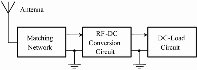
Figure 1. Schematic view of a RF energy harvesting system.
energy conversion module can be used to energize the low power devices for example sensors for a sensor network in application to agriculture.
Section 2 of this paper discusses on the theoretical background of the voltage doubler circuit. Section 3 presents the simulation study and implementation of the circuit design. Section 4 provides the results and analysis. Section 5 concludes with a discussion on the findings from the simulated and measured results.
2. Voltage Multiplier
There are various voltage multiplier circuit topologies. The design used in this module is derived from the function of peak detector or a half wave peak rectifier. The Villard voltage multiplier circuit was chosen in the circuit design of this paper because it produces two times of the input signal voltage towards ground at a single output and can be cascaded to form a voltage multiplier with an arbitrary output voltage and its design simplicity.
2.1. Diode Modeling
The voltage multiplier circuit in this design uses zero bias Schottky diode HSMS-2850 from Agilent. The attractive feature of these Schottky diodes are low substrate losses and very fast switching but leads to a fabrication overhead. This diode has been modeled for the energy harvesting circuit which comes in a one-diode configuration. The modeling parameters for these diodes are given by Agilent in their data sheets. These parameters are used in Multisim for its own modeling purposes. The modeling is done by transforming the diode into an equivalent circuit using passive components which are described by the SPICE parameters in Table 1 [6].
The diode used in this design is shown in Figure 2 and its equivalent model is shown in Figure 3. The special features of HSMS-2850 diode is that it provides a low forward voltage, low substrate leakage and uses the non
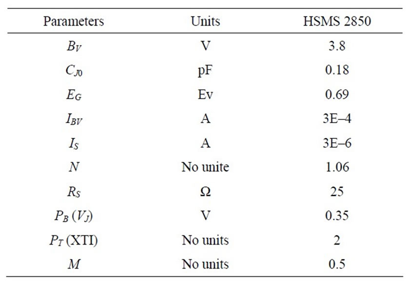
Table 1. SPICE parameters.
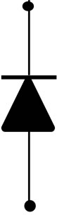
Figure 2. Schottky diode.
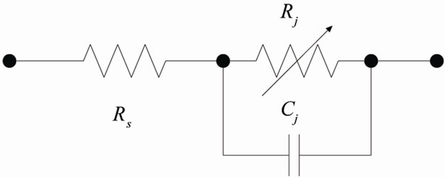
Figure 3. Linear circuit model of the Schottky diode [6].
symmetric properties of a diode that allows unidirectional flow of current under ideal condition.
The diodes are fixed and are not subject of optimization or tuning. This is described using the following derivations. By neglecting the effect of diode substrate, an equivalent linear model that can be used for the diode as shown in Figure 3. When Cj is the junction capacitance and Rj is the junction resistance, the admittance Yz of the linear model is given by
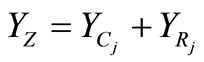 (1)
(1)
Equation (1) related to the frequency of operation is given by
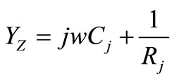 (2)
(2)
 (3)
(3)
The impedance Z of the linear model is given by
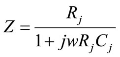 (4)
(4)
The total impedance ZT is given by
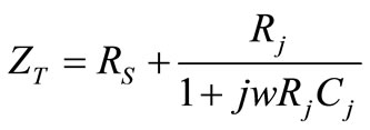 (5)
(5)
where RS is the series resistance of the circuit and Rj is given by
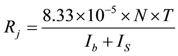
where:
Ib = bias current in µA;
Is = saturation current in µA;
T = temperature (K);
N = ideality factor.
In Equation (5), Rj and Cj are constants and the frequency of operation (w) is the only variable parameter. As the frequency increases, the value of Z is almost negligible compared to the series resistance RS of the diode. From this it is concluded that the function of the diode is independent of the frequency of operation.
2.2. Single Stage Voltage Multiplier
Figure 4 represents a single stage voltage multiplier circuit. The circuit is also called as a voltage doubler because in theory, the voltage that is arrived on the output is approximately twice that at the input. The circuit consists of two sections; each comprises a diode and a capacitor for rectification. The RF input signal is rectified in the positive half of the input cycle, followed by the negative half of the input cycle. But, the voltage stored on the input capacitor during one half cycle is transferred to the output capacitor during the next half cycle of the input signal. Thus, the voltage on output capacitor is roughly two times the peak voltage of the RF source minus the turn-on voltage of the diode.
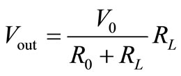
The most interesting feature of this circuit is that when these stages are connected in series. This method behaves akin to the principle of stacking batteries in series to get more voltage at the output. The output of the first stage is not exactly pure DC voltage and it is basically an AC signal with a DC offset voltage. This is equivalent to a DC signal superimposed by ripple content. Due to this distinctive feature, succeeding stages in the circuit can get more voltage than the preceding stages. If a second stage is added on top of the first multiplier circuit, the only waveform that the second stage receives is the noise of the first stage. This noise is then doubled and added to the DC voltage of the first stage. Therefore, the more stages that are added, theoretically, more voltage will come from the system regardless of the input. Each independent stage with its dedicated voltage doubler circuit can be seen as a single battery with open circuit output voltage V0, internal resistance R0 with load resistance RL, the output voltage, Vout is expressed as in Equation (7).
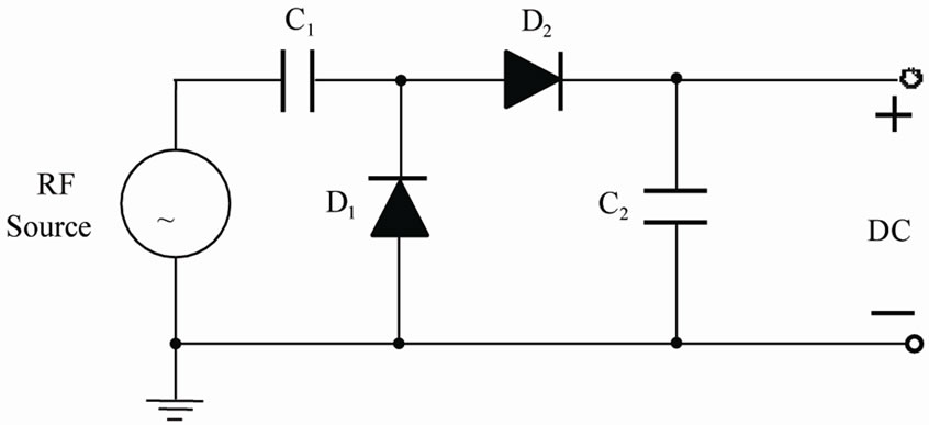
Figure 4. Single stage voltage multiplier circuit [7].
 (6)
(6)
When n number of these circuits are put in series and connected to a load of RL in Equation (6) the output voltage Vout obtained is given by this change in RC value will make the time constant longer which in turn retains the multiplication effect of two in this design of seven stage voltage doubler.
 (7)
(7)
The number of stages in the system has the greatest effect on the DC output voltage, as shown from Equations (6) and (7).
It is inferred that the output voltage Vout is determined by the addition of  and
and , if V0 is fixed. From this analysis it is observed that V0, R0 and RL are all constants. Assume that V0 = 1 V,
 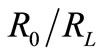 = 0.25, n = 2, 3, 4, 5, 6 and 7, the output voltage Vout = 1.33 V, 1.72 V, 2.0 V, 2.22 V, 2.43 V and 2.56 V respectively when substituted analytically in the Equation (7). This analysis can be compared with the results obtained in the circuit design of this module. In simulation at n = 4, Vout = 1.42 V, n = 5, Vout = 1.67 V; n = 6, Vout = 1.92; n = 7, Vout = 2.15 V; n = 8, Vout = 1.92 V; n = 9, Vout = 1.81 V. Also in measurement, for n = 4, Vout = 2.1 V; n = 5, Vout =2.9 V; n = 6, Vout = 3.72 V; and n = 7, Vout = 5 V. As n increases, the increase in output voltage will be almost double the input voltage up to some number of stages. But at some point, i.e. beyond seven stages, in this circuit the output voltage gained (8 and 9 stages) will be negligible as shown in Figure 5.
The capacitors are charged to the peak value of the input RF signal and discharge to the series resistance (Rs) of the diode. Thus the output voltage across the capacitor of the first stage is approximately twice that of the input signal. As the signal swings from one stage to other, there is an additive resistance in the discharge path of the
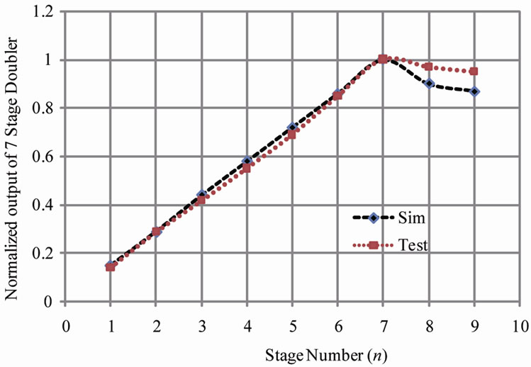
Figure 5. Normalized output voltage multiplier versus number of stages.
diode and increase of capacitance due to the stage capacitors.
2.3. Seven Stage Voltage Multiplier
The seven stage voltage multiplier circuit design implemented in this paper is shown in Figure 6. Starting on the left side, there is a RF signal source for the circuit followed by the first stage of the voltage multiplier circuit. Each stage is stacked onto the previous stage as shown in the Figure 6. Stacking was done from left to right for simplicity instead of conventional stacking from bottom to top.
The circuit uses eight zero bias Schottky surface-mount Agilent HSMS-285X series, HSMS-2850 diodes. The special features of these diode is that, it provides a low forward voltage, low substrate leakage and uses the nonsymmetric properties of a diode that allows unidirectional flow of current under ideal conditions. The diodes are fixed and are not subject of optimization or tuning. This type of multiplier produces a DC voltage which depends on the incident RF voltage. Input to the circuit is a predefined RF source. The voltage conversion can be effective only if the input voltage is higher than the Schottky forward voltage.
The other components associated with the circuit are the stage capacitors. The chosen capacitors for this circuit are of through-hole type, which make it easier to modify for optimization, where in [8] the optimization was accomplished at the input impedance of the CMOS chip for a three stage voltage multiplier. The circuit design in this paper uses a capacitor across the load to store and provide DC leveling of the output voltage and its value only affects the speed of the transient response. Without a capacitor across the load, the output is not a good DC signal, but more of an offset AC signal.
In addition to the above, an equivalent load resistor is connected at the final node. The output voltage across the load decreases during the negative half cycle of the AC input signal. The voltage decreases is inversely proportional to the product of resistance and capacitance across the load. Without the load resistor on the circuit, the voltage would be hold indefinitely on the capacitor and look like a DC signal, assuming ideal components. In the design, the individual components of the stages need not to be rated to withstand the entire output voltage. Each component only needs to be concerned with the relative voltage differences directly across its own terminals and of the components immediately adjacent to it. In this type of circuitry, the circuit does not change the output voltage but increases the possible output current by a factor of two. The number of stages in the system is directly proportional to the amount of voltage obtained and has the greatest effect on the output voltage as explained in the Equation (7) and shown in Figure 5.
3. Simulation and Implementation
Multisim software was chosen for modeling and simulation which is a circuit simulation tool by Texas Instruments. The simulation and practical implementation were carried out with fixed RF at 945 MHz ± 100 MHz, which are close to the down link center radio frequency (947.5 MHz) of the GSM-900 transmitter. The voltages obtained at the final node VDC of the multiplier circuit were recorded for various input power levels from –40 dBm - +5 dBm with power level interval (spacing) of 5 dBm.
The simulations were also carried out using same stage capacitance value (3.3 nF) and then with a varied capacitance value for all stages from 4 stages through 9 stages [9]. The capacitance value was varied in such a way that, from one stage to the next, it was halved. For example, if the first stage was 3.3 nF, the second stage was 1.65 nF, third stage was 825 pF, fourth stage was 415 pF and so on. But keeping in view of testing, the capacitance values were chosen to have a close match with the standard available values in the market.
Simulation was carried out through 4 to 9 voltage doubler stages. Based on results obtained a 7 stage doubler is best to implemented for this application.
The design of the printed circuit board (PCB) was carried out using DipTrace software. The material used to
Figure 6. Schematic of 7 stage voltage multiplier.
manufacture the printed circuit board (PCB) is the standard Fiberglass Reinforced Epoxy (FR4), with the thickness of 1.6 mm and dielectric constant of 3.9. The topology is constructed on the PCB with the dimensions of 98 mm × 34 mm (W × H). The Sub Miniature version A (SMA) connectors are used at the input and output of PCB to carry out the measurements. The circuit components consist of active and passive components. The component used in circuit is shown in Table 2.
Special handling precautions have been taken to avoid Electro Static Discharge (ESD), while assembling of the surface-mount zero bias Schottky diodes. Also special attention has been given to mount other components and the SMA connectors on to the PCB. The Photograph of Assembled circuit board I shown in Figure 7.
4. Results and Analysis
The simulated and measured results at the output voltage of voltage multiplier circuit are shown graphically in Figure 8. From the graph analysis, the simulated and the measured results agree considerably with each other. The measured results are shown to be better than the simulation results. The reason behind this may be due to the uncertainty in series resistance value of the diode obtained from SPICE parameters in modeling as explained in Equation (5). This resistance vale of diodes in practical circuit may be lower than in the model, which provides fast discharge path, in turn rise in voltage as passes through the stages and reaches to final output. In this work, the DC output voltages obtained through simulation and measurement at 0 dBm re 2.12 V and 5.0 V respectively. These results are comparatively much better than in ref. [9], where in at 0 dBm, 900 MHz they achieved 0.5 V and 0.8 V through simulation and measurement respectively.
Figures 9 and 10 show the result of a 4 stage voltage doubler circuit with equal and varied capacitance values between the stages as described in Section 3.
From the analysis of these two simulations, it can be observed that the resulting output voltages are equal. The only difference between these two graphs is the rise time of the circuit with varied capacitance value is a little bit slower. But, overall result on the performance of rise time is still under 20 µs to 24 µs and the difference is negligible. From these results, the use of equal stage capacitance of each being 3.3 nF was hence considered for the design of the multiplier.
The results from Figure 11, shows that the output voltage reaches to 1.0 V within 20 µS and then uniformly increasing to 1.4 V, 1.67 V, 1.87 V and 2.12 V for 4, 5, 6 and 7 stages respectively compared to 2 mS as shown in [10]. Figure 12 shows that the conversion ratio of 22 is achieved at 0 dBm input power and drops to 2.5 at –40 dBm. The highest value at 0 dBm is due to the innate characteristics of the zero bias Schottky diodes which conduct fairly well at higher input voltages.
5. Conclusion
From the experimental results, it is found that the pro-
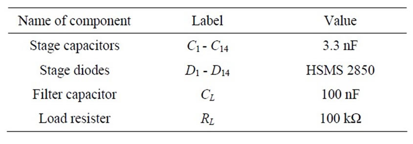
Table 2. Component used in 7 stage voltage multiplier.
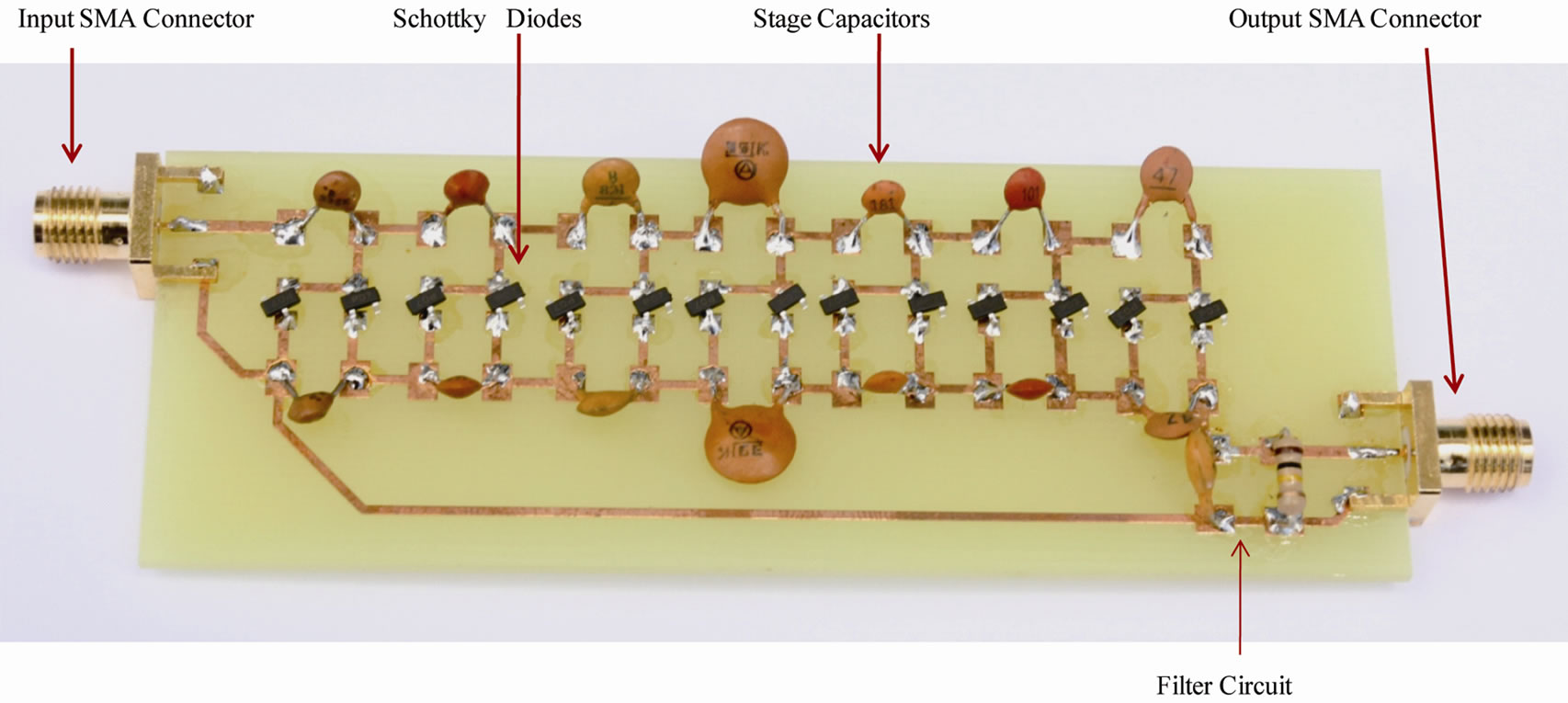
Figure 7. Photograph of assembled circuit board.
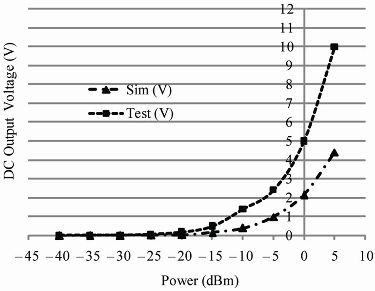
Figure 8. Simulated and test DC output voltage of multiplier as a function of input power.
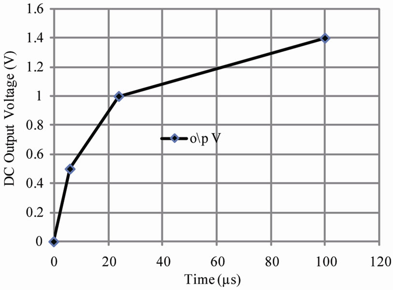
Figure 9. DC output voltage verses rise time of 4 stage voltage doubler circuit with equal stage capacitance [8].
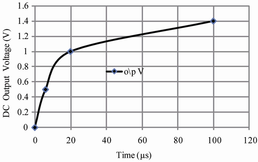
Figure 10. DC output voltage verses rise time of 4 stage voltage doubler with varied stage capacitance [8].
posed voltage multiplier circuit operates at the frequency of 945 MHz with the specified input power levels. The results have shown that there is multiplication of the input voltage. From Figure 12, it is shown that at 0 dBm input power, the multiplication factor is 22. This is sig-

Figure 11. DC output voltage verses rise time of voltage doubler circuit through 4 - 7 stages with equal stage capacitance.
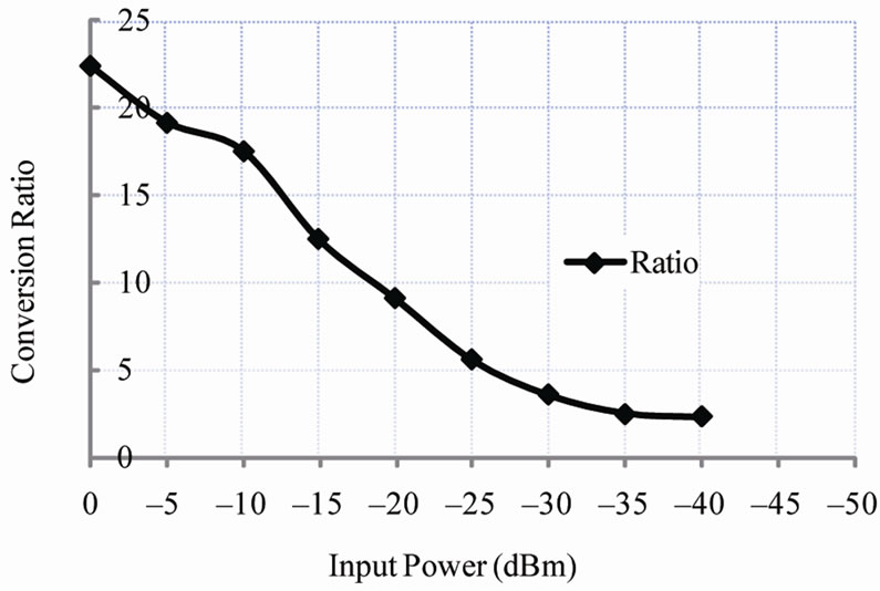
Figure 12. Conversion ratio as a function of input power.
nificant, as the work shows that RF energy in the GSM- 900 band can be harvested from the ambient RF source using the Villard circuit topology. The power density levels from a GSM base station is expected from 0.1 mW/m2 to 1 mW/m2 for a distance ranging from 25 m - 100 m. These power levels may be elevated by a factor between one and three for the GSM-900 downlink frequency bands depending on the traffic density [10]. The next phase of the research work is to interface the voltage multiplier circuit through a matching network to the antenna at the input side and a low power device to power from the system at the output side to complete the RF energy harvesting system.
6. Acknowledgements
We would like to acknowledge and thank the Ministry of Higher Education Malaysia for funding this project under Fundamental Research Grant: FRGS/1/10/TK/UNITEN/ 02/13.
REFERENCES
- S. von der Mark and G. Boeck, “Ultra Low Power Wakeup Detector for Sensor Networks,” SBMO/IEEE MTT-S International Microwave & Optoelectronics Conference (IMOC 2007), Berlin, 29 October-1 November 2007, pp. 865-868. doi:10.1109/IMOC.2007.4404394
- H. Yan, J. G. M. Montero, A. Akhnoukh, L. C. N. de Vreede and J. N. Burghartz, “An Integration Scheme for RF Power Harvesting,” Proceedings of STW Annual Workshop on Semiconductor Advances for Future Electronics and Sensors, Veldhoven, November 2005, pp. 64-66. doi:10.1.1.126.5786
- T. Ungan and L. M. Reindl, “Concept for Harvesting Low Ambient RF-Sources for Microsystems,” 2007. http://www.imtek.de/content/pdf/public/2007/powermems_2007_paper_ungan.pdf
- J. Wang, L. Dong and Y. Z. Fu, “Modeling of UHF Voltage Multiplier for Radio-Triggered Wake-Up Circuits,” International Journal of Circuit Theory and Application, Vol. 39, No. 11, 2010, pp. 1189-1197. doi:10.1002/cta.692
- J. A. Starzyk, Y.-W. Jan and F. J. Qiu, “A DC-DC Charge Pump Design Based on Voltage Doublers,” IEEE Transactions on Circuits and Systems-I: Fundamental Theory and Applications, Vol. 48, No. 3, 2001, pp. 350-359.
- HSMS-2850, “Surface Mount Zero Bias Schottky Detector Diodes.” http://www.crystal-radio.eu/hsms285xdata.pdf
- D. W. Harrist, “Wireless Battery Charging System Using Radio Frequency Energy Harvesting,” M.S. Thesis, University of Pittsburgh, Pittsburgh, 2004.
- E. Bergeret, J. Gaubert, P. Pannie and J. M. Gaultierr, “Modeling and Design of CMOS UHF Voltage Multiplier for RFID in an EEPROM Compatible Process,” IEEE Transactions on Circuits and Systems-I, Vol. 54, No. 10, 2007, pp. 833-837. doi:10.1109/TCSII.2007.902222
- B. Emmanuel, J. Gaubert, P. Pannier and J. M. Gaultier, “Conception of UHF Voltage Multiplier for RFID Circui,” IEEE North-East Workshop on Circuits and Systems, Gatineau, June 2006, pp. 217-220. doi:10.1109/NEWCAS.2006.250961
- H. J. Visser, A. C. F. Reniers and J. A. C. Theeuwes, “Ambient RF Energy Scavenging: GSM and WLAN Power Density Measurements,” Proceedings of the 38th European Microwave Conference, Eindhoven, 27-31 October 2008, pp. 721-724. doi:10.1109/EUMC.2008.4751554
NOTES
*Corresponding author.