Journal of Modern Physics
Vol.3 No.8(2012), Article ID:21677,8 pages DOI:10.4236/jmp.2012.38089
Deposition and Characterisation of Nitrogen-Doped Zinc Oxide Thin Films by MOCVD Using Zinc Acetate—Ammonium Acetate Precursor
1Department of Physics, Federal University of Technology, Owerri, Nigeria
2Department of Physics, Obafemi Awolowo University, Ile-Ife, Nigeria
3Centre for Energy Research and Development, Obafemi Awolowo University, Ile-Ife, Nigeria
4Department of Chemistry, Obafemi Awolowo University, Ile-Ife, Nigeria
Email: *eobajayi@yahoo.co.uk
Received May 4, 2012; revised June 1, 2012; accepted June 25, 2012
Keywords: Zinc Oxide; Thin Films; N-Doping; Precursor; Characterisation
ABSTRACT
The synthesis and comprehensive analysis of nitrogen-doped zinc oxide thin films grown from a compound precursor of zinc acetate and ammonium acetate has been reported. The precursor was processed in different ratios of the zinc acetate-ammonium acetate additives, and each combination was used to deposit a thin film using metalorganic chemical vapour deposition (MOCVD) method. The produced thin films were characterised using Rutherford backscattering (RBS) spectroscopy, uv-visible spectrometry, x-ray diffractometry, four point probe measurements and optical microscopy. The deposited thin films showed a fairly consistent zinc:oxygen:nitrogen ratio of 4.4:3.7:1, the film structures were quasicrystalline and the sheet resistivities were high, while other familiar characteristics like optical transmittance, bandgap, thermal stability, etc. were maintained in the grown films. Applications in device fabrication and active sensor devices were hence envisaged as the emergent potentials of the thin films.
1. Introduction
Zinc oxide thin films have in the present time assumed a formidable focus and an utmost importance in technological applications. The most striking of the applications are in electronics, piezoelectricity, spintronics, sensor devices, coatings, etc. [1-5]. These stem from their several favorable properties, viz, good transparency, high electron mobility, wide bandgap, large exciton binding energy, strong room-temperature luminescence, good age and thermal stability, etc. [6-8]. The thin films are obtainable through virtually all the thin film production processes including physical, chemical and sputtering methods and some of their combinations.
The raw materials for ZnO thin films vary, and largely depend on the production process and material availability. The material and process of fabrication will of course determine the reproducibility and price of the end-product. In this wise it has been found that most of the sophisticated methods of production end up at research level, while the very simple methods are largely unreplicable or do not meet the requirements for device fabrication.
Dopability is another vital consideration in the choice of process and raw material [7,9]. For example it is usually difficult to directly dope thin films produced by the physical and sputtering processes, save perhaps by diffusion or other secondary process.
In this work an adapted MOCVD method was used to deposit nitrogen-doped ZnO thin films from a compound precursor of zinc acetate and ammonium acetate. The thin films, which were deposited on glass substrate, were characterised and their properties were established.
2. Experimental Details
Ammonium acetate was introduced into zinc acetate in respective amounts of 10%, 20%, 30% and 40%. Each mixture was processed into a dry powder by repeatedly grinding and spreading in a mortar, and placing in the oven at about 50˚C. The powders were in turn placed at the bobbling compartment of an MOCVD set up and compressed air at a flow rate of 2.5 dm3/minute was used to bobble the particles through a preheating furnace to the cracking furnace at a temperature of 420˚C, while working pressure was atmospheric all through. Soda-lime glass slides were used as the substrates and their coatings were carried out for two hours respectively for each powder set up. For easy identification, the coatings were designated as A1, A2, A3 and A4 for the thin films emanating from the 10%, 20%, 30% and 40% ammonium acetate compositions respectively.
Retrieved coatings were characterised by RBS spectroscopy, uv spectrometry, x-ray diffractometry, four-point probe measurements and optical microscopy.
A tandem accelerator was used for the RBS measurements of the thin films. The measurements carried out include the elemental composition, atomic ratio, depth profile and thickness.
Jenway 6405 UV-Vis spectrophotometer was used for the optical characterizations. Using the machine, the transmittance of each coating was measured in the wavelength range of 320 nm to 1100 nm. The reading of each coating was established by subtracting the reading of an uncoated substrate from the coated one.
X-ray diffraction was done with RC MD 10 diffractometer using Cu Kα rays as its primary x-ray tool. The blank substrate was first scanned and its reading respectively subtracted from those of the coated substrates. The equipment recorded the refracted pulses against the diffraction angles (2θ), from which the respective refraction peaks, crystal structures, molecular structures and fullwidth at half-maxima (FWHM) of the coatings were established.
The sheet resistivity of the thin films were measured using a Lucas Signatone four-point probe on a Keithley 237 voltage equipment. Silver pastes were first deposited at four points, approximately at the corners of 1 cm2 on the surface of each sample, as specified by the van-derpauw arrangement. The deposited pastes (contacts) were then cured at low temperature (approximately 50˚C) for 24 hours before the conductivity tests were carried out. The I-V characteristics of each sample were taken 2 - 3 times depending on the adaptability of the equipment for the sample, with the current and voltage points being swapped in each setting as is customary in the measurement. The average of each set of readings was taken and the familiar formula
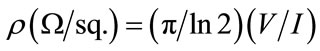 (1)
(1)
used to calculate the sheet resistivity ⍴ of the coatings.
Olympus APT 2000 optical microscope was used to picture the surface structure of each thin film sample. The micrograph of each sample was taken at 100× magnification. The images were then processed using ImageJ software. With the processing, both two-dimensional and three-dimensional views of each of the surfaces were obtainable. Scale lines serving as magnification keys were placed on each processed micrograph with the help of grid lines enabled by the software to aid in grain size estimation.
3. Results and Discussion
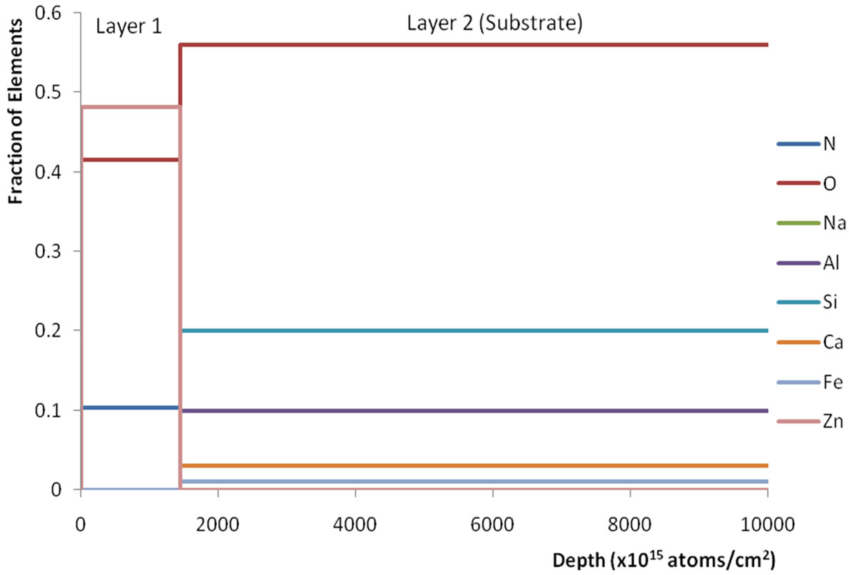
Figure 1" target="_self">Figure 1 shows the RBS spectrum and Figure 2" target="_self">Figure 2 the depth profile of sample A1. Both the spectrum and the profile depict two distinct sections, the substrate section and the thin film (coating) section, beginning from about 1450 keV energy, or covering up to about 1400 × 1015 atomic layers, respectively. The presence of only Zn, O and N in the coating section and in characteristic proportions are also clearly manifested. The RBS displays of the other samples are similar, and a summary of these charactariistics is displayed in Table 1.
112-bfa8-2e8e635bbd95.jpg" width="833.43498840332" height="419.61501159668 " />
Figure 1" target="_self">Figure 1. RBS spectrum of sample A1.
 1159668" height="5
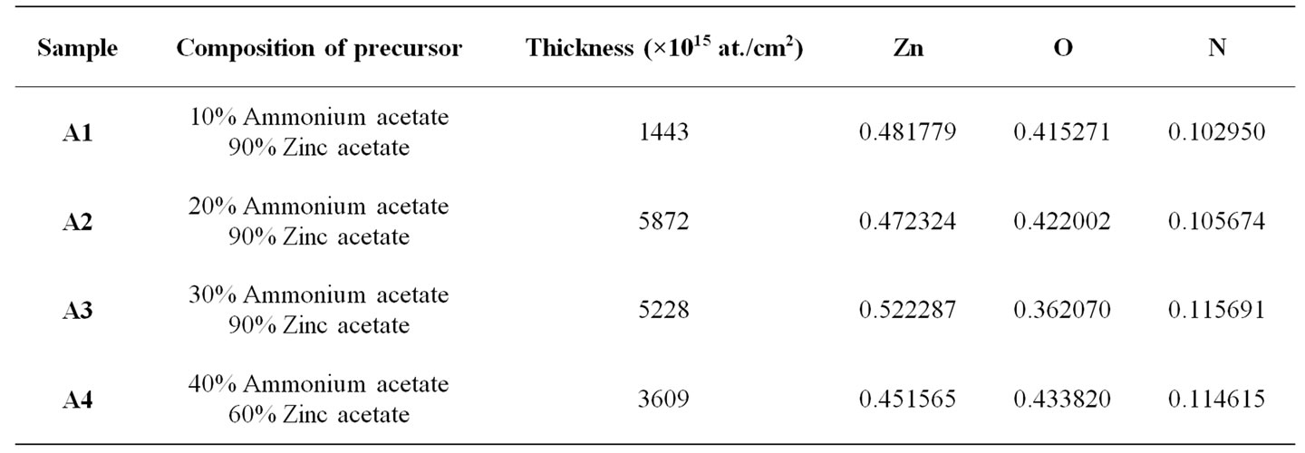
Table 1. RBS characteristics of deposited thin films.
The RBS results exhibit no visible trend with respect to the sample compositions. It can be observed, however, that the elements in all the specimens maintained a fairly constant ratio, which on the average is Zn:O:N = 4.3924:3.7208:1 ≈ 4.4:3.7:1. A notable feature of the RBS result is that the proportion of nitrogen consumed in each deposition process is fairly constant, irrespective of the proportion of ammonium acetate (providing the nitrogen) in the prevailing precursor. This suggests the possibility of a threshold in the ratio of ammonium acetate to zinc acetate in the precursor, beyond which the amount of nitrogen incorporated does not vary. This threshold ratio will most likely be in single digit percentage or even a fraction of one percent, since the focus is on the nitrogen as a dopant to the zinc oxide thin film.
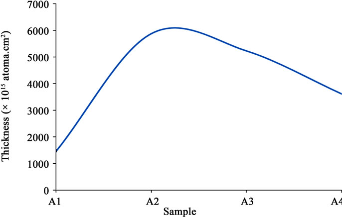
The thickness trend contained in Table 1 is plotted in Figure 3" target="_self">Figure 3. It can be observed that the thickness of sample A1 and sample A4 are small relative to those of sample A2 and sample A3. The variation in thicknesses is attributable to the quantity of precursor used for the respective depositions, and the position of the substrates in the deposition chamber. In some previous works on the thickness of ZnO thin films perused [10,11], there was no correlation with other properties of the material.
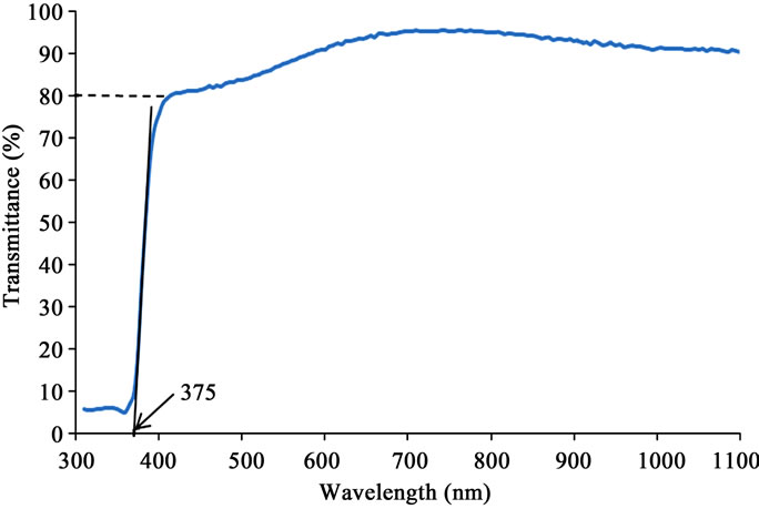
The uv-visible transmission spectrum for sample A1 is displayed in Figure 4" target="_self">Figure 4. The spectra for the other samples are similar, and show clearly that the deposited thin films were all over 80% transparent to the visible spectrum. The transmittance peaked at different levels above 93% for the different compositions. The trend is shown in Table 2.
The intercepts of the transmittance spectra were extrapolated with straight lines at the inflexion points between the ultraviolet and visible portions of the spectra as shown in Figure 4" target="_self">Figure 4. The process gave respective intercepts at 375 nm for sample A1, 380 nm for sample A2, 380 nm for sample A3, and 375 nm for sample A4. These intercepts correspond to the respective absorption edges for the specimens. From the intercepts therefore the band edges or energy gaps were calculated according to Planck’s equation
11e5b11-7602-4958-bc72-68a15252ac42.jpg" width="246.525" height="69.825" /> (2)
with the value of λ inserted for each reading and the result divided by electronic charge, e = 1.602 × 10⁻¹⁹, the energy gaps, Eg, were obtained in units of electronvolt, eV. The outcome of these calculations is also displayed in Table 2.
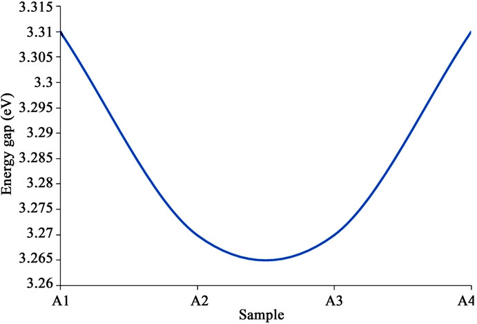
One observes some kind of trend in the transmittance and the bandgap vis-à-vis the composition. That is, the transmittance appeared to increase with increase in ammonium acetate content, stabilize, and then started to reduce as the content increased further (Figure 5" target="_self">Figure 5); for the bandgap, it decreased with increase in ammonium acetate
content, stabilized, and then started to increase with further increase in the content (Figure 6" target="_self">Figure 6). These were respectively in consonance and opposite with the trend in thickness.
Several workers have reported energy gap of ZnO in the range 3.2 to 3.3 eV, while reported transmittance have hovered around 85%, with some reporting as high as over 95% as in this work [10,12]. These results for optical transmittance and energy bandgap therefore tallied well with those of the other workers. Therefore the grown thin films from the precursor arrangement are very promising for solid state and optoelectric applications.
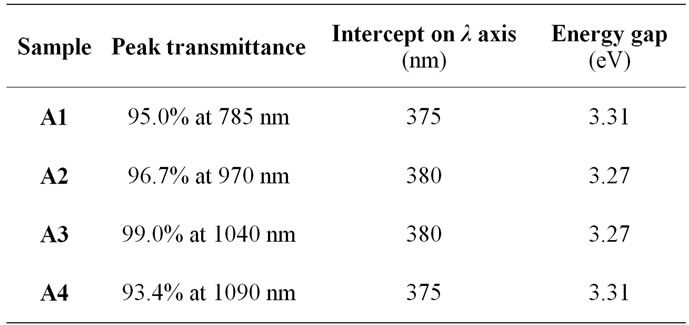
Table 2. Optical and electronic characteristics of deposited thin films.
11bc8-9946-4784-b38e-f6b6d6c3ebae.jpg" width="440.325" height="309.225 " />
Figure 5" target="_self">Figure 5. Peak transmittance of the samples.
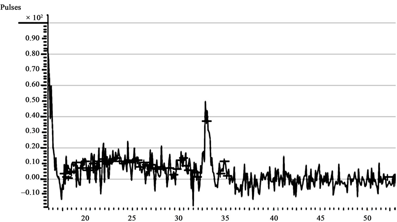
In Figure 7" target="_self">Figure 7 is the XRD spectrum of sample A1. The spectrum is almost diffuse, with tiny spikes all over. A prominent characteristic peak is however on display, and occurred at about 2θ = 32.9˚. This result falls in line with the established range for the characteristic diffraction peak of the substance. The other samples gave a similar display. The XRD results depict low intensity diffractions [13], with the random peaks occurring at different crystallographic planes and accompanying fullwidth at half-maxima (FWHM). The results suggest that the films were partly polycrystalline and partly quasicrystalline, and thus the crystal structures were not quite explicit [13-15].
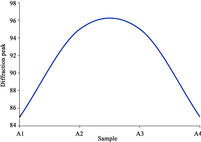
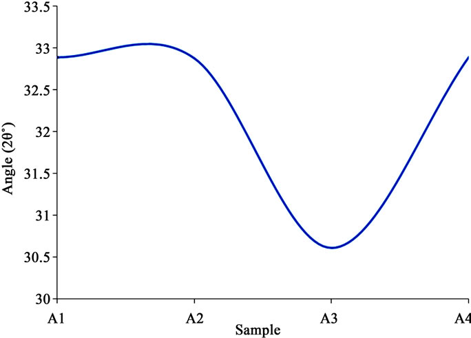
There were here also some trends in the structure characteristics of the specimens in relation to their compositions. The most prominent peaks increased from low ammonium acetate to higher, stabilized, and then decreased again as the composition increased (Figure 8" target="_self">Figure 8). Conversely, the peak angles decreased with increasing ammonium acetate content, and then began to increase again as the content continued to increase (Figure 9" target="_self">Figure 9). This tended to tally with the trends in the results for thickness under RBS, and then transmittance, and bandgap under the optical and electronic characteristics. The XRD results suggest that the peaks were due to ZnO, and this is substantiated by other workers who proved that such peaks became more distinct upon annealing the samples, with more peaks emerging in the process [16-18]. The porous morphology and stable semi-amorphous structure however, have potential application for sensing of oxygen and other gaseous species when made part of conventional, heated metal oxide sensor devices [13].
 11.58498840332" height="453.24500579834 " />
Figure 7" target="_self">Figure 7. XRD spectrum of sample A1 (The Abscissa represents 2θ˚).
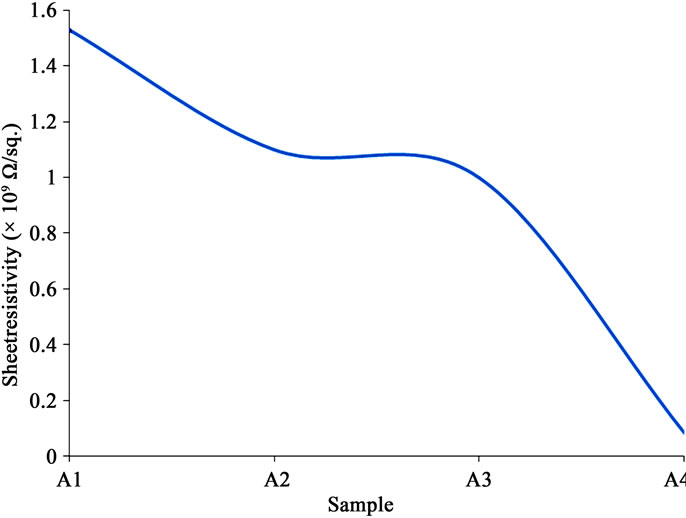
Sheet resistivities obtained for the thin films were 1.53 × 10⁹ Ω/sq. for sample A1, 1.10 × 10⁹ Ω/sq. for sample A2, 1.00 × 10⁹ Ω/sq. for sample A3, and 8.00 × 10⁷ Ω/sq. for sample A4. Some other workers have also obtained resistivity results of similar order [10,13,15,16,19]. Joseph et al. (1999) partially attributed high resistivity to columnar growth on the film surface. But the majority opinion was that the quasicrystalline nature of the films was responsible for the trend in their sheet resistivities. This view was confirmed as some of these workers went further to anneal their films, thereby paving way for the realignment of the grain boundaries. In the process they obtained films with increased crystallinity and enhanced conductivity [13,16]. This is applicable to the thin films of this study if one chooses to anneal. Li (2003), however, recommended only rapid thermal anneal (RTA) in such case, since under conventional anneal process the nitrogen atoms coalesce and form bubbles, giving way to voids on the film surface.
The resistivity decreased sharply from sample A1 to A2, almost leveled between A2 and A3, and then decreased more sharply between A3 and A4. These suggest some enhancement of conductivity with increase in the amount of ammonium acetate in the precursor. Figure 1" target="_self">Figure 10 shows the trend in the sheet resistivity of the samples.
The high resist property of the thin films tend to reemphasise their potential as active semiconducting elements for gas sensors as well as touch sensors. Joseph et al. (1999) reported high resistivity for nitrogen-doped ZnO thin films and which were of p-type. Maksimov (2010) also attributed the high resistivity of his N-doped ZnO thin films to its p-type character. These results propound a high probability that the thin films of this work are of p-type, and if so, a readily available path for achieving cheap fabrication of optoelectric and sensing semiconductor devices would has been struck.
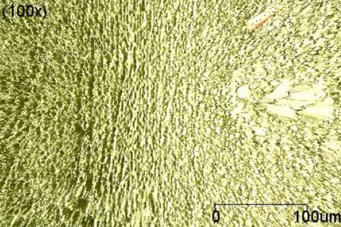
The micrographs of sample A1 is displayed in Figure
11. The figure showed a non-uniform cluster of grains, some of the clusters forming large lumps with sizes larger than 30 μm. The trend in the other samples followed suit. with annealing at slightly elevated temperature, the grains may re-align to give more uniform films with enhanced properties [10,11].
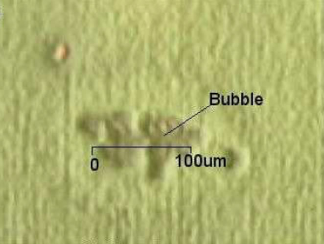
Some nitrogen gas bubbles similar to those reported by Li (2003) were observed on some of the film surfaces. Few of these degenerated into prominent craters measuring up to 50 μm as shown in Figure 1" target="_self">Figure 12.
The voids were possibly contributory to the high resistivity of the thin films. Higher magnification with the optical micrographs showed what looked like columnar growth, which are indicative of the hexagonal nature of the ZnO thin films with c-axis orientation, and useful for piezoelectric and spintronic applications [20].
4. Conclusions
From this work a cheap and easily replicable means of producing direct N-doped ZnO thin films was realized, using a finely divided compound precursor of zinc acetate and ammonium acetate.
The thin films produced had good age and thermal
stability. Their optical and electronic characteristics were maintained, but most other traditional properties were violated, leading to more interesting applicabilities. In particular, the films were found to be semi-amorphous or quasicrystalline with scanty columnar growth, and the sheet resistivities were high. Excess nitrogen coalesced into bubbles and escaped, as the proportion of nitrogen in the thin films remained fairly constant irrespective of the content of ammonium acetate in each precursor producing it.
High-tech applicabilities of the thin films have also been discussed. Applications of particular interest include gas and touch sensors, transparent resistors, piezoelectricity and spintronics.
5. Acknowledgements
The authors are grateful to the following: authorities of the Departments of Physics and Chemistry, Obafemi Awolowo University, Ile-Ife for allowing the use of their equipments and laboratory facilities; Centre for Energy Research and Development (CERD), Obafemi Awolowo University, Ile-Ife for RBS and XRD analyses; Central Laboratory, Obafemi Awolowo University, Ile-Ife for uv-visible analyses, and Engineering Materials Development Institute (EMDI), Akure for uv-visible, XRD, resistivity and microscopy analyses. Our profound gratitude also goes to Dr. A. I. Akinwande of the Department of Electrical Engineering and Computer Science, Massachusetts Institute of Technology, Cambridge for resistivity analyses and other parallel characterizations.
REFERENCES
- D. Look, “Recent Advances in ZnO Materials and Devices,” Materials Science and Engineering: B, Vol. 80, No. 1-3, 2001, pp. 383-387. doi:10.1016/S0921-5107(00)00604-8
- S. O. Kucheyev, “Ion-beam-produced structural defects in ZnO,” Physical Review B, Vol. 67, No. 9, 2003, Article ID: 094115. 1103/PhysRevB.67.094115"> doi:10.1103/PhysRevB.67.094115
- H. T. Wang, B. S. Kang, F. Ren, L. C. Tien, P. W. Sadik, D. P. Norton, S. J. Pearton and J. Lin, “Hydrogen-Selective Sensing at Room Temperature with ZnO Nanorods,” Applied Physics Letters, Vol. 86, No. 24, 2005, Article ID: 243503. doi:10.1063/1.1949707
- Science Daily, “New Small-scale Generator Produces Alternating Current by Stretching Zinc Oxide Wires,” Science Daily, 2008. http://www.sciencedaily.com/releases/2008/11/081109193342.htm
- Access Data, “Database of Select Committee on GRAS Substances, SCOGS) Reviews,” 2009. http://www.accessdata.fda.gov/scripts/fcn/fcnDetailNavigation.cfm?rpt=scogsListing&id=372
- U. Rossler,“New Series, Group III. Vol. 17B, 22, 41B,” Springer, Heidelberg, 1999.
- Ü. Özgür, Y. I. Alivov, C. Liu, A. Teke, M. A. Reshchikov, S. Doğan, V. Avrutin and S. J. Cho, “A Comprehensive Review of ZnO Materials and Devices,” Journal of Applied Physics, Vol. 98, No. 4, 2005, Article ID: 041301. doi:10.1063/1.1992666
- A. C. Mofor, A. El-Shaer, A. Bakin, A. Waag, H. Ahlers, U. Siegner, S. Sievers and M. Albrecht, “Magnetic Property Investigations on Mn-Doped ZnO Layers On Sapphire,” Applied Physics Letters, Vol. 87, No. 6, 2005, Article ID: 062501. doi:10.1063/1.2007864
- T. Ohgaki, N. Ohashi, S. Sugimura, H. Ryoken, I. Sakaguchi, Y. Adachi and H. Haneda, “Positive Hall Coefficients Obtained from Contact Misplacement on Evident N-Type ZnO Films and Crystals,” Journal of Materials Research, Vol. 23, No. 9, 2008, pp. 2293-2295. doi:10.1557/jmr.2008.0300
- J. S. Wellings, N. B. Chaure, S. N. Heavens and I. M. Dharmadasa, “Growth and Characterisation of Electrodeposited ZnO Thin Films,” Thin Solid Films, Vol. 516, No. 12, 2007, pp. 3893-3898. doi:10.1016/j.tsf.2007.07.156
- B. Sang, A. Yamada and M. Konagai, “Highly Stable ZnO Thin Films by Atomic Layer Deposition,” Japanese Journal of Applied Physics, Vol. 37, 1998, pp. L1125-L1128. 1143/JJAP.37.L1125">doi:10.1143/JJAP.37.L1125
- V. Srikant and D. R. Clarke, “Optical Absorption Edge of ZnO Thin Films: The Effect of Substrate,” Journal of Applied Physics, Vol. 81, No. 9, 1997, pp. 6357-6364. doi:10.1063/1.364393
- S. O’Brien, M. G. Nolan, M. Copuruglu, J. A. Hamilton, Povey, I. Pereira, L. Martins, R. Fortunato and E. Pemble, “Zinc oxide thin films: Characterisation and Potential Applications,” Thin Solid Films, Vol. 518, No. 16, 2010, pp. 4515-4519. doi:10.1016/j.tsf.2009.12.020
- S. T. Tan, B. J. Chen, X. W. Sun, M. B. Yu, X. H. Zhang and S. J. Chua, “Realization of Intrinsic p-Type ZnO Thin Films by MOCVD,” Journal of Electronic Materials, Vol. Vol. 34, No. 8, 2005, pp. 1172-1176. 11664-005-0247-6"> doi:10.1007/s11664-005-0247-6
- O. Maksimov, “Recent Advances and Novel Approaches of p-Type Doping of Zinc Oxide,” Reviews on Advanced Materials Science, Vol. 24, No. 1-2, 2010, pp. 26-34.
- S. X. Li, “Nitrogen Doped Zinc Oxide Thin Film, Nitrogen Doped Zinc Oxide Thin Film,” Master’s Thesis, University of California, Berkeley, 2003. http://www.repositories.cdlib.org/lbnl/LBNL-541166
- E. Fortunato, P. Barquinha, A. Pimentel, A. Gonçalves, L. Pereira, A. Marques and R. Martins, “Next Generation of Thin Film Transistors Based on Zinc Oxide,” Materials Research Society, Vol. 811, 2004. 11-E1.9"> doi:10.1557/PROC-811-E1.9
- J. Weng, Y. Zhang, G. Han, Y. Zhang, L. Xu, J. Xu, X. Huang and K. Chen, “Electrochemical deposition and characterization of Wide Band Semiconductor Zno Thin Film,” Thin Solid Films, Vol. 478, No. 1-2, 2005, pp. 25- 29. doi:10.1016/j.tsf.2004.09.047
- M. Joseph, H. Tabata and T. Kawai, “p-Type Electrical Conduction in ZnO Thin Films by Ga and N Codoping,” Japanese Journal of Applied Physics, Vol. 38, 1999, pp. L1205-L1207. 1143/JJAP.38.L1205">doi:10.1143/JJAP.38.L1205
- W. L. Dang, Y. Q. Fu, J. K. Luo, A. J. Flewitt and W. I. Milne, “Deposition and Characterization of Sputtered ZnO Films,” Superlattices and Microstructures, Vol. 42, No. 1-6, 2007, pp. 89-93. doi:10.1016/j.spmi.2007.04.081
NOTES
*Corresponding author.