Wireless Engineering and Technology
Vol.2 No.1(2011), Article ID:3791,8 pages DOI:10.4236/wet.2011.21003
Capacitive Model and S-Parameters of Double-Pole Four-Throw Double-Gate RF CMOS Switch
![]()
1Department of Electronics and Communication Engineering, Jaypee University of Information Technology, Solan, India; 2VLSI Design Group, Central Electronics Engineering Research Institute, Pilani, India.
Email: viranjay@ieee.org
Received September 28th, 2010; revised November 9th, 2010; accepted November 11th, 2010.
Keywords: Capacitive Model, Double-Gate MOSFET, DP4T Switch, Isolation, Radio Frequency, RF Switch, S-Parameter and VLSI
ABSTRACT
In this paper, we have analyzed the Double-Pole Four-Throw Double-Gate Radio-Frequency Complementary Metal-Oxide-Semiconductor (DP4T DG RF CMOS) switch using S-parameters for 1 GHz to 60 GHz of frequency range. DP4T DG RF CMOS switch for operation at high frequency is also analyzed with its capacitive model. The results for the development of this proposed switch include the basics of the circuit elements in terms of capacitance, resistance, impedance, admittance, series equivalent and parallel equivalent of this network at different frequencies which are present in this switch whatever they are ON or OFF.
1. Introduction
Continuous scaling of CMOS technology has now reached to a state of evolution, in terms of both frequency and noise, where it is becoming a rigorous part for RF applications at high frequency region of the system. The aggressive scaling of metal-oxide-semiconductor field effect transistors (MOSFET) has led to the fabrication of high performance with a cut-off frequency more than 150 GHz. As a result of this development, the CMOS is a strong candidate for RF wireless communications in the GHz frequency range. The excellent improvement in the frequency response of silicon CMOS devices in recent years has motivated their use in millimeter-wave applications.
Saha [1] solved a problem of critical issue with the continued scaling of MOSFET devices towards their ultimate dimensions near 10 nm regime, and define the process variability induced device performance variability has become a critical issue in the design of very large scale integrated (VLSI) circuits using advanced CMOS technologies. Manku [2] has discussed the design issues and the microwave properties of CMOS devices with qualitative understanding of the microwave characteristics of the MOS transistors which is helpful for IC circuit design to create better front-end radio-frequency CMOS circuits and presented the network properties of CMOS devices, the frequency response, the microwave noise properties and scaling rule. Mekanand et al. [3] have proposed a transceiver CMOS switch for 2.4 GHz with low insertion loss and excellent control voltage. These simulation results of CMOS switch design demonstrate an insertion loss of 1.102 dB for receiving mode and 1.085 dB for transmitting mode. Both modes can operate using a control voltage of only 1.2 V. Srivastava [4] design a model for a capacitor device using MOS layers with an oxide thickness of 528 Å (measured optically), and measured the material parameters from the curve drawn between capacitance and voltage through the Visual Engineering Environment Programming (VEE Pro) software. In this research, to find good result, vary the voltage with smaller increments and perform the measurements. Litwin [5] has presented a model for gate resistance (Rg) component in silicided polysilicon gate MOSFETs and discussed the high frequency properties depend critically on Rg, which has motivated the recent addition of a resistive gate input in the BSIM3v3 MOSFET model. These results show that the contact resistance between silicide and polysilicon, built into the gate of a typical MOSFET, is of the same magnitude as the silicide sheet resistance. Srivastava et al. [6,7] presented a model for a capacitor device, oxide thickness of 510 Å (measured optically), measures the oxide thickness by the SUPREM simulator. Its accuracy depends on the quality of models, parameters and numerical techniques it employ and also verify the result by measurement of capacitance at different voltages using LCR meter. Based on this oxide thickness measurement of a MOS capacitor, one can measure the device parameters, mainly the substrate dopant concentration.
Ye and Cao [8] realized that the random variations have been regarded as one of the major barriers on CMOS scaling and proposed a compact 3-D model and perform the atomistic simulations to investigate fundamental variations in a scaled CMOS device, including random dopant fluctuation (RDF), line edge roughness (LER), and oxide thickness fluctuation (OTF). These models are scalable with device specifications, enabling quantitative analysis of circuit performance variability in future technology nodes. Caverly et al. [9] fabricated some cells using standard processes of 2.0 µ, 1.2 µ and 0.8 µ CMOS integrated circuit with no post-processing performed. The results indicate that 2.0 µm CMOS can be used successfully up to approximately 0.25 GHz with 0.8 µm cells useful up to approximately 1 GHz. Srivastava et al. [10] investigated the design parameters of RF CMOS cells which is suitable for switch in the wireless telecommunication systems and this results for the development of a cell library which includes the basics of the circuit elements required for the radio frequency sub-systems of the integrated circuits such as V-I characteristics at low voltages, contact resistance which is present in the switches and the potential barrier with contacts available in devices.
Moldovan, et al. [11] demonstrated the capability of undoped Double-Gate (DG) MOSFET explicit and analytical compact model, to forecast the effect of the volume inversion on the intrinsic capacitances. For that purpose, Moldovan simulated the results for these capacitances, which presents an accurate dependence on the silicon layer thickness, consistent with twodimensional numerical simulations, for both thin and thick silicon films. Also, even if the current drive and trans-conductance are enhanced in volume inversion regime, this compact model results that intrinsic capacitances are higher as well, which may limit the highspeed (delay time) behavior of DG MOSFETs under volume inversion regime. Huang [12] fabricated a Single-Pole Double-Throw (SPDT) transceiver switch for 3.0 V for a 0.5 μ CMOS process. This analysis shows that substrate resistances and source/drain-to-body capacitances must be lowered to decrease insertion loss. This switch exhibits a 0.7 dB insertion loss, a 17 dBm power 1 dB compression point (P1 dB), and a 42 dB isolation at 928 MHz. The switch has adequate insertion loss, isolation, P1 dB, and IP3 for 900 MHz ISM band applications requiring a moderate peak transmitter power level (~15 dBm). Hamed et al. [13] emphasized on use of independently driven nano-scale DG MOSFETs for low power analog circuits and satisfied that in independent drive configuration, the top gate response of DG MOSFETs can be altered by application of a control voltage on the bottom gate.
Srivastava, et al. [14] proved that to avoid the uses of multiple RF chain associated with the multiple antennas (used to replace traditional single antennas circuitry in the radio transceiver system in order to improve the transmission capability and reliability), RF switch is most essential component. So in [14] we proposed a Double-Pole Four-Throw (DP4T) RF switch using CMOS technology with inverter property. Due to these advantages, we extend this design for a DP4T DG RF CMOS switch and intend its equivalent network circuit to realize S-parameters after that measured the performance parameter as isolation, VSWR and returns loss in an RF system. The RF switch with CMOS especially striking for various applications because it allows integration of both digital and analog functionality on the same die and increasing performance which is due to double-gate MOSFET. In the design of DP4T DG RF CMOS switch structures for digital and analog, a transaction between speed and frequency response and circuit complexity is always encountered. Applications for a CMOS switch also covers the areas of micro power circuits and other wireless applications at frequencies from 1 GHz to 60 GHz.
In this paper, we present a comprehensive study S-parameter for the low-power, high speed DP4T DG RF CMOS switch. The DP4T DG RF CMOS switch structures with its capacitive models are studied to understand the effect of device geometry on the working of switching properties. The organization of the paper is as follows. The DP4T DG RF CMOS switch model is presented in the Section 2. The capacitive model of DP4T DG RF CMOS switch is discussed in the Section 3. The S-parameters of the DP4T DG RF CMOS switches are discussed in the Section 4. Finally, Section 5 concludes the work.
2. DP4T RF CMOS Switch Model with
Double-Gate
Since connecting an n-channel MOSFET in parallel with a p-channel MOSFET allows signals to pass in either direction. Whether the n-channel or the p-channel device carries more signal current depends on the ratio of input to output voltage. Because the switch has no preferred direction for current flow, it has no preferred input or output. In this section, we have designed a DP4T RF CMOS switch structures using double-gate MOSFET as shown in Figure 1 for low power consumption and low distortion for application of RF switch in communication that operates between 1 GHz to 60 GHz. This switch exhibit high isolation to avoid mixing of received signals at a particular time [15].
This switch contains double-gate n-MOSFET in its main architecture which is shown in Figure 1 and its layout using a design tool Microwind 3.0 version is shown in Figure 2, similarly, we can the design doublegate p-MOSFET. This switch circuit is designed with a Micro-Cap Evaluation 6.0 tool. In this switch, transmitted signal from power amplifier is sent to transmitter through double-gate p-MOSFET to transmitter named as A_Tx and B_Tx, here two identical double-gate p-MOSFET are used and received signal which travel from the antenna through double-gate n-MOSFET to the receiver named as A_Rx and B_Rx, two identical double-gate n-MOSFET. The switch designed here is suitable to drive 50 Ω resistive loads and utilized multiple gate fingers to reduce the parasitic capacitance. This
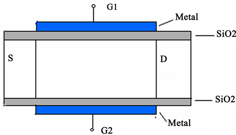
Figure 1. Basic double gate n-MOSFET.
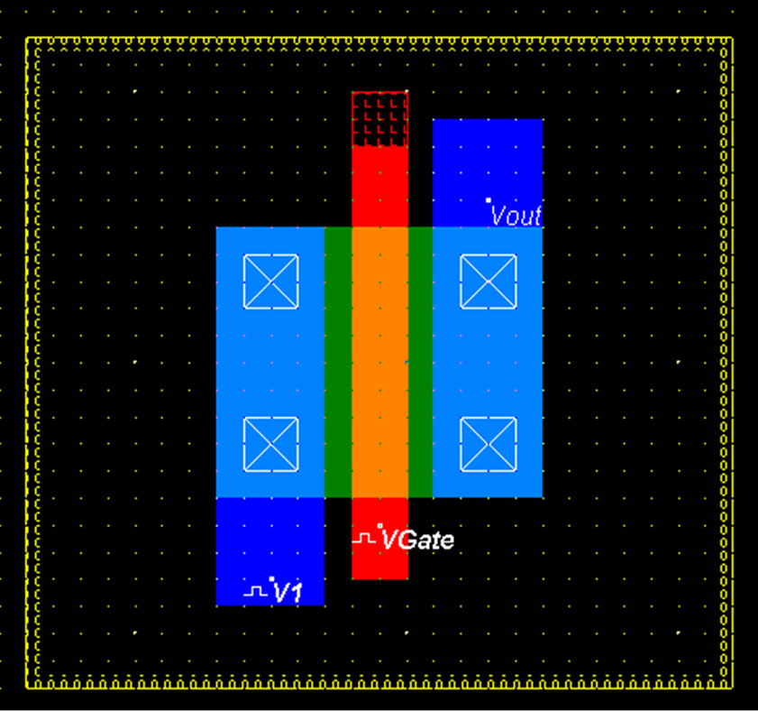
Figure 2. Layout of the Double-Gate (DG) MOSFET.
switch requires only two control lines (V1, V2) of 1.2 V to control the signal congestion between two antennas and four ports. Signal fading effects can be reduced with this DP4T DG RF CMOS switch because sending identical signals through multiple antennas will most likely result in a high quality combined signal at the receiver end.
In DP4T switch as shown in Figure 3, four transistors are used for two antennas. In this antenna by using the CMOS functionality, at a time any one of transistor M1 or M3 will operate and in the same fashion any one of transistor M2 or M4 will operate as these are combination of n-MOSFET and p-MOSFET and supply voltage is either zero or 2.1 V.
3. Capacitive Model of DP4T DG RF CMOS Switch
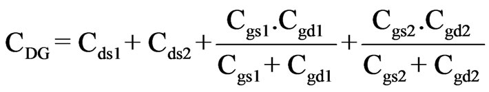
The capacitive models of a DP4T DG RF CMOS Switch is biased in linear region, at the ON state of switch, here at a time only one transistor will be ON either doublegate n-MOSFET or double-gate p-MOSFET. The capacitive model for a double-gate n-MOSFET is shown in Figure 4. For the given design of DP4T DG RF CMOS switch capacitance model under the operating condition is shown in Figure 5. Here we consider the ON status, because the insertion loss is conquered by its ON-resistance and substrate resistance [16,17]. Isolation of the switch is finite due to signal coupling through the parasitic and junction capacitances. For double gate MOSFET at cutoff region, resistance RON1, RON2 will become zero. For maximum capacitance, assuming all the capacitances is present at a time. In the double-gate MOSFET, parasitic capacitances are Cds1, Cds2, Cgs1, Cgs2, Cgd1 and Cgd2 and junction capacitances are not present as bulk that is not available in this MOSFET.
For DG MOSFET when both the transistors are ON, Csb and Cdb are not present so fewer signals being coupled to the substrate as substrate is not present in this structure, so no dissipation in the substrate resistance Rb. When the transistor is in cut-off region, increasing Cds1,
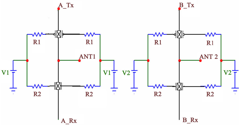
Figure 3. DP4T DG RF CMOS switch proposed by [14].
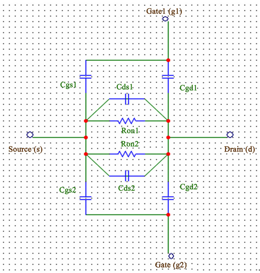
Figure 4. Model of the double gate n-MOSFET transistor operating as a switch at ON state.
Cds2, Cgd1, Cgd2, Cgs1 and Cgs2 leads to higher isolation between the source and drain due to no capacitive coupling between these terminals. At the transistors cut-off region Cds, Cgd and Cgs increases, which directs to lower isolation between the source and drain due to capacitive coupling between these terminals [18]. In Figure 4, for DG MOSFET, the total maximum capacitance across source to drain is given by (1).
 (1)
(1)
For the model of a DP4T DG RF CMOS switch at ON state the total capacitance will be individual capacitance of a particular transistor as any one transistor will be ON at a time which are calculated for double-gate nMOSFET and double-gate p-MOSFET as given by (2) and (3) respectively;
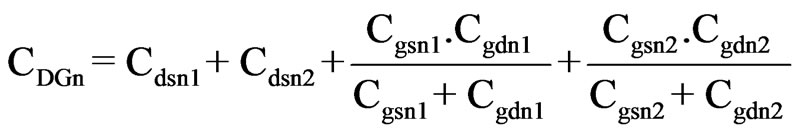 (2)
(2)
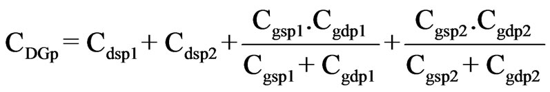 (3)
(3)
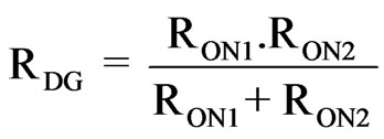
And the ON-resistance will be combination of resistances due to gate 1 (g1) and gate 2 (g2), which are parallel resultant.
 (4)
(4)
where,
 (5)
(5)
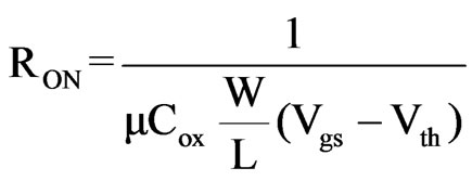
Since by the calculation of capacitances with (1) and (2), we concludes that if the value of capacitances are increases, then isolation will become better in DP4T DG RF CMOS switch compare to already existing DP4T RF CMOS switch. Also the resistance RON is parallel combination of RON1 and RON2 which moves total resistance down and helps in fast current movement and increases the speed of switch. For appropriate working of a switch and to reduce the insertion loss, we can also achieve reduction in ON-resistance with choosing transistor with large μ, increasing W/L, keeping Vgs – Vth large as clear from (5) [19, 20].
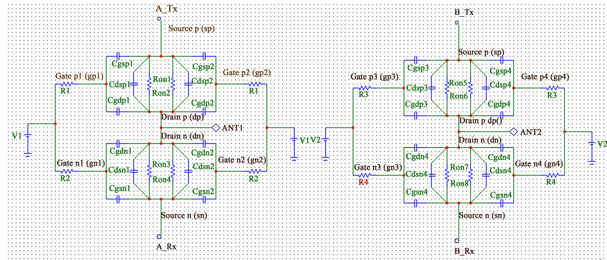
Figure 5. Capacitive model of the DP4T DG RF CMOS switch at ON state.
4. S-Parameters of the DP4T DG RF CMOS Switch
S-parameters describe the response of an N-port network to voltage signals at each port. It has magnitude as well as phase information means gain or loss and phase shift information and it is a powerful way to describe an electrical network. S-parameters change with frequency, load impedance, source impedance and network.
For an example, authors have considered each available capacitance in Figure 5, of a 1 fF for DP4T DG RF CMOS switch, and then it gives total capacitance of CDG of a 3 fF with help of (1). With this capacitance we design a network of switch as shown in Figure 6, with RF Sim-99, free available software. Here the tolerance of total capacitance is consider as +2% to –2%. At frequency band of 0.8 GHz to 60 GHz, we found noise power of –173.83 dBm with return loss 10 dB, transmission loss 0.46 dB, VSWR 1.93:1, reflection coefficient 0.316, system impedance 50 ohm [21]. We analyze this DP4T DG RF CMOS equivalent switch for 1 GHZ, 2.5 GHz, 5 GHZ, 10 GHz, 25 GHz, 50 GHz and 60 GHz of frequency [22-27]. These parameters are summarizes in the Table 1.
Smith chart is a graphical aid, designed for RF engineering to assist in solving problems with transmission lines and matching circuits. Use of the Smith chart utility has grown steadily over the years and it is still widely used today, not only as a problem solving aid, but as a graphical demonstrator of how many RF parameters behave at one or more frequencies, an alternative to using tabular information. The Smith chart is used here to represent impedance, admittance, reflection coefficient, scattering parameter, noise figure circle, constant gain contours and regions for unconditional stability. The Smith chart is most frequently used at or within the unity radius region.
Table 2 shows the impedance, admittance, series equivalent and parallel equivalent of this network at 1 GHz to 60 GHz frequencies. After designing this network
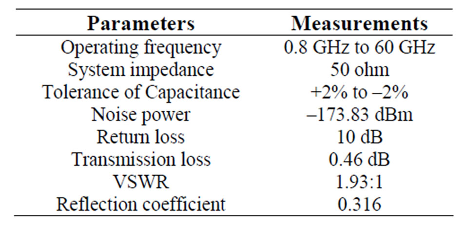
Table 1. Measured parameters for DP4T DG RF CMOS switch.
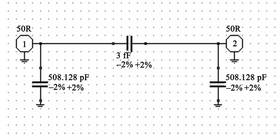
Figure 6. Equivalent circuit of the DP4T DG RF CMOS switch.
of switch, we can draw the curve for S-parameters which are shown in Figure 7 and Figure 8. With the help of this curve, we tabularize the S11, S12, S21 and S22 in Table 3, at the above stated frequencies. These values of S-parameter give magnitude of S12 and S21 in terms of dB as shown in Table 4.
From the Table 2 it is revealed that the impedance, admittance, series equivalent and parallel equivalent decreases with the increase in frequency. But the series equivalent capacitance and parallel equivalent capacitance are fixed at 508.13 pF whatever the value of frequency. Also characteristics of impedance, admittance, series equivalent and parallel equivalent inverted with the increase in frequency.
From the Table 3 it has been concluded that at no signal, the entire unpredictable signal returned back, means no any unwanted signal passes the switch because
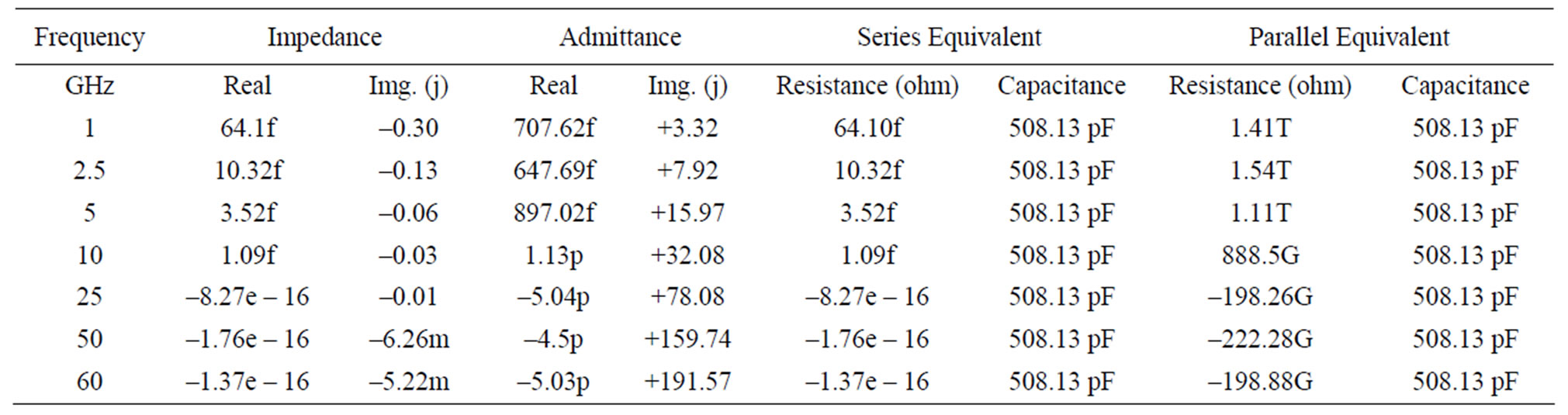
Table 2. Impedance, admittance, series equivalent and parallel equivalent.
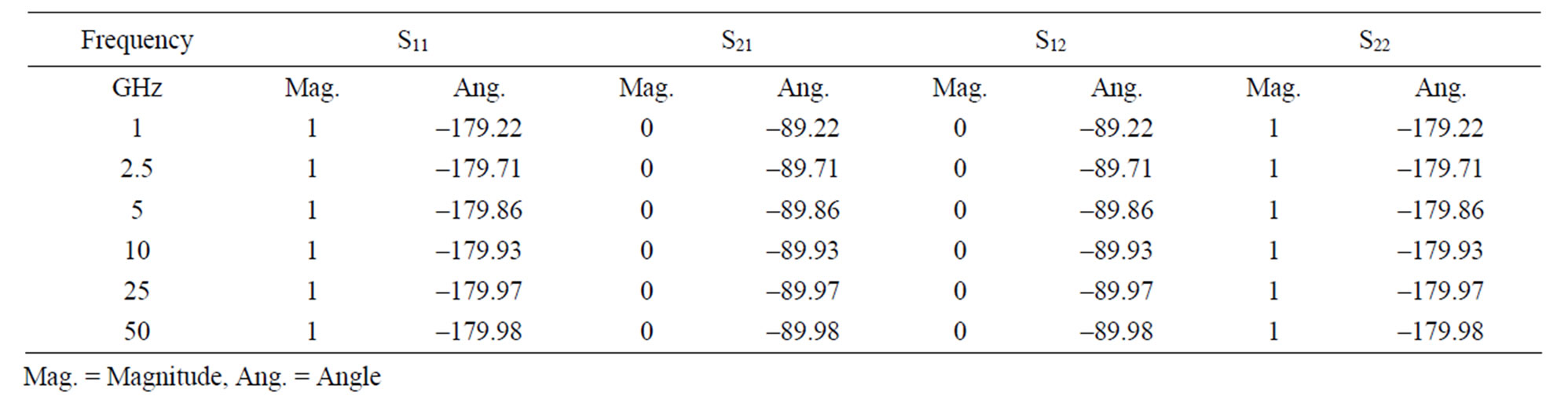
Table 3. S-parameters of a designed switch at different frequencies.
Figure 7. Measurements of S11 and S22, for DP4T DG RF CMOS switch.
Figure 8. The S12 and S21 parameters of the DP4T DG RF CMOS switch.
S11 and S22 are 1 and at same time S12 and S21 is zero. Also with increase in frequency we achieve a fine angle. This table also concludes that the maximum amplitude and minimum amplitude of the resultant signal occurs when the reflected wave is in phase and 180 degree out of phase
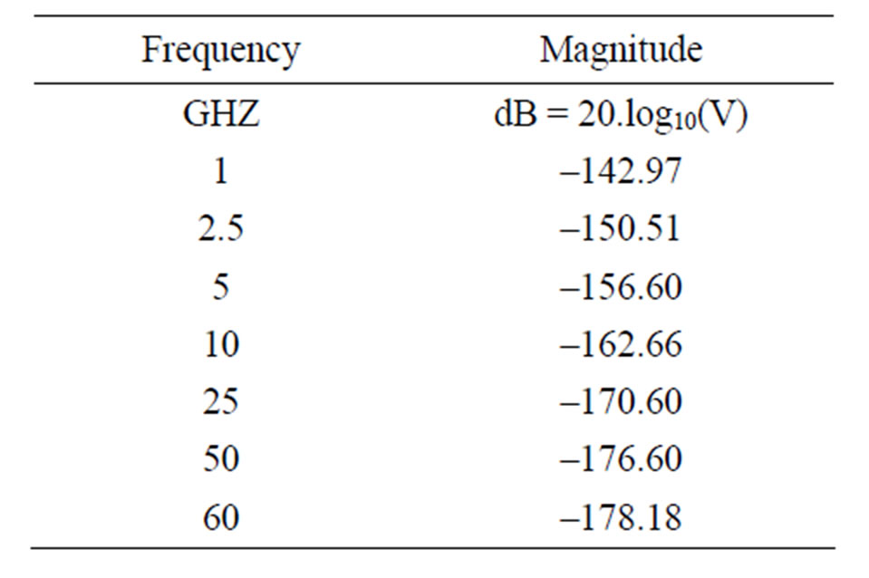
Table 4. Magnitude of S12 and S21 (both are equal) at different frequencies.
with the input signal, respectively. The reflected wave, when summed with the input signal either increases or decreases its net amplitude, depending on whether the reflection is in phase or out of phase with the input signal.
From the Table 4, it is accomplished that the magnitude in terms of dB decreases with increase in frequencies. We can also measure the reflection, VSWR (ratio of the maximum reflected wave (in phase) to minimum reflected wave (out of phase) voltages in the standing wave), return loss (a measure of the power of the reflected signal) [18], also a subset of insertion loss as higher the return loss (or reflections) in an RF system, the higher its insertion loss from these conclusion.
5. Conclusions
For the proposed capacitive model of the DP4T DG RF CMOS switch, the equivalent circuit and simulated S-parameters are presented. It includes the basics of the circuit elements parameter required for the RF sub-systems of the integrated circuits such as ON resistance, parasitic capacitances, S-parameters, impedance, admittance, series equivalent and parallel equivalent. By using these results, we can calculate the return loss, transmission loss, VSWR. For the purpose of a RF switch, we achieve the process to minimize the ON resistance and maximize the parasitic capacitance to control the isolation and switching speed. Since here we discussed the parameters for 1 GHz to 60 GHz operating frequencies of the RF switches so this is useful for IEEE 802.11 industrial applications including Wi-Fi.
REFERENCES
- S. K. Saha, “Modeling Process Variability in Scaled CMOS Technology,” IEEE Journal of Design and Test of Computers, Vol. 27, No. 2, 2010, pp. 8-16. doi:10.1109/ MDT.2010.50
- T. Manku, “Microwave CMOS Device Physics and Design,” IEEE Journal of Solid State Circuits, Vol. 34, No. 3, 1999, pp. 277-285. doi:10.1109/4.748178
- P. Mekanand, P. Prawatrungruang and D. Eungdamrong, “0.5 µ CMOS 2.4 GHz RF Switch for Wireless Communications,” Proceedings of 10th International Conference on Advanced Communication Technology, Phoenix Park, 17-20 February 2008, pp. 447-450. doi:10.1109/ICACT. 2008.4493799
- V. M. Srivastava, K. S. Yadav and G. Singh, “Application of VEE Pro Software for Measurement of MOS Device Parameter Using C-V Curve,” International Journal of Computer Applications, Vol. 1, No. 7, 2010, pp. 43-46. doi:10.5120/164-289
- A. Litwin and A. B. Stockholm, “Overlooked Interfacial Silicide-Polysilicon Gate Resistance in MOS Transistors,” IEEE Transactions on Electron Devices, Vol. 48, No. 9, 2001, pp. 2179-2181. doi:10.1109/16.944214
- V. M. Srivastava, K. S. Yadav and G. Singh, “Measurement of Oxide Thickness for MOS Devices, Using Simulation of SUPREM Simulator,” International Journal of Computer Applications, Vol. 1, No. 6, 2010, pp. 66-70. doi:10.5120/141-260
- V. M. Srivastava, “Relevance of VEE Programming for Measurement of MOS Device Parameters,” Proceedings of IEEE International Advance Computing Conference, Patiala, 6-7 March 2009, pp. 205-209.
- Y. Ye and Y. Cao, “Random Variability Modeling and Its Impact on Scaled CMOS Circuits,” Journal of Computational Electronics, Vol. 9, No. 3-4, 2010, pp. 108-113. doi:10.1007/s10825-010-0336-5
- R. H. Caverly, S. Smith and J. Hu, “RF CMOS Cells for Wireless Applications,” Journal of Analog Integrated Circuits and Signal Processing, Vol. 25, No. 1, 2001, pp. 5-15. doi:10.1023/A:1008365816788
- V. M. Srivastava, K. S. Yadav and G. Singh, “Designing Parameters for RF CMOS Cells,” International Journal of Circuits and Systems, Vol. 1, No. 2, 2010, pp. 49-53. doi:10.4236/cs.2010.12008
- O. Moldovan, F. A. Chaves, B. Iñiguez, et al., “Accurate Prediction of the Volume Inversion Impact on Undoped Double-Gate MOSFET Capacitances,” International Journal of Numerical Modeling, Electronic Networks, Devices and Fields, Vol. 23, No. 6, 2010, pp. 447-457. doi:10.10 02/jnm.745
- F. J. Huang, “A 0.5 μm CMOS T/R Switch For 900 MHz Wireless Applications,” IEEE Journal of Solid-State Circuits, Vol. 36, No. 3, 2001, pp. 486-492. doi:10.1109/4. 910487
- H. Hamed, S. Kaya and J. Starzyk, “Use of Nano-Scale Double-Gate MOSFETs in Low Power Tunable Current Mode Analog Circuits,” Journal of Analog Integrated Circuits, Signal Processing, Vol. 54, No. 3, 2008, pp. 211-217. doi:10.1007/s10470-008-9134-4
- V. M. Srivastava, K. S. Yadav and G. Singh, “DoublePole Four-Throw Switch Design with CMOS Inverter,” Proceeding of 5th IEEE International Conference on Wireless Communication and Sensor Network, Allahabad, 15-19 December 2009, pp. 1-4. doi:10.1109/WCSN.2009. 5434786
- A. V. Garcia, S. Reynolds and J. O. Plouchartv, “60 GHz Transmitter Circuits in 65 nm CMOS,” Radio Frequency Integrated Circuits Symposium, 2008, pp. 641-644. doi: 10.1109/RFIC.2008.4561519
- S. H. Lee, C. S. Kim and H. K. Yu, “A Small Signal RF Model and Its Parameter Extraction for Substrate Effects in RF MOSFETs,” IEEE Transaction on Electron Devices, Vol. 48, No. 7, 2001, pp. 1374-1379. doi:10.110 9/16.930654
- S. Sharma and P. Kumar, “Non Overlapped Single and Double-Gate SOI/GOI MOSFET for Enhanced Short Channel Immunity,” Journal of Semiconductor Technology and Science, Vol. 9, No. 3, 2009, pp. 136-147.
- S. Kang and Y. Leblebici, “CMOS Digital Integrated Circuits Analysis and Design,” 3rd Edition, McGraw Hill, New York, 2002.
- T. H. Lee, “The Design of CMOS Radio-Frequency Integrated Circuits,” 2nd Edition, Cambridge University Press, New York, 2004.
- R. Baker, H. Li and D. Boyce, “CMOS Circuit Design, Layout, and Simulation,” 3rd Edition, IEEE Press Series on Microelectronic Systems, USA, 2010.
- Y. Cheng and M. Matloubian, “Frequency Dependent Resistive and Capacitive Components in RF MOSFETs,” IEEE Electron Device Letters, Vol. 22, No. 7, 2001, pp. 333-335.
- J. P. Carmo, P. M. Mendes, C. Couto and J. H. Correia “A 2.4 GHz RF CMOS Transceiver for Wireless Sensor Applications,” Proceeding of International Conference on Electrical Engineering, Coimbra, 7-10 October 2005, pp. 902-905.
- V. M. Srivastava, K. S. Yadav and G. Singh, “Design and Performance Analysis of Double-Gate MOSFET over Single-Gate MOSFET for RF Switch,” Journal of Microelectronics, in press, 2010. doi:10.1016/j.mejo.2010. 12.007
- Y. Cheng and M. Matloubian, “Parameter Extraction of Accurate and Scalable Substrate Resistance Components in RF MOSFETs,” IEEE Electron Device Letters, Vol. 23, No. 4, 2002, pp. 221-223. doi:10.1109/55.992845
- P. H. Woerlee, “RF CMOS Performance Trends,” IEEE Transaction on Electron Devices, Vol. 48, No. 8, 2001, pp. 1776-1782. doi:10.1109/16.936707
- V. M. Srivastava, K. S. Yadav and G. Singh, “DoublePole Four-Throw CMOS Switch Design With DoubleGate Transistor,” 2010 Annual IEEE India Conference, Kolkata, 17-19 December 2010, in press.
- C. Ta, E. Skafidas and R. Evans, “A 60-GHz CMOS Transmit/Receive Switch,” IEEE Radio Frequency Integrated Circuits Symposium, Hawaii, 3-5 June 2007, pp. 725-728. doi:10.1109/RFIC.2007.380985