Graphene
Vol. 1 No. 2 (2012) , Article ID: 23963 , 4 pages DOI:10.4236/graphene.2012.12004
Characterization of Nanometer-Spaced Few-Layer Graphene Electrodes
Kavli Institute of Nanoscience, Delft University of Technology, Delft, The Netherlands
Email: E.BurzuriLinares@tudelft.nl
Received August 8, 2012; revised September 17, 2012; accepted October 10, 2012
Keywords: Graphene; Spintronics; Three-Terminal Transistors
ABSTRACT
We study graphene electrodes that can be used for contacting single molecules. The nanometer-scale gap is made by feedback controlled electroburning in few-layer graphene sheets. We analyze the time stability, and the influence of the temperature and gate voltage on the current flowing through the empty gaps. The electrodes are stable at room temperature for long periods of time. We show statistics of the relation between the initial resistance of the few-layer graphene flakes and the final size of the gaps. We find that thicker flakes are more suitable for the fabrication of the electrodes.
1. Introduction
Graphene, extensively studied in the last years, has emerged as a material of special interest for spintronics. Being an all organic material, it displays unique electronic transport properties [1] such as high carrier mobility, high flexibility and very low spin-orbit coupling which allows the injection of spin-polarized currents in graphene with very long coherence lengths even at room temperatures [2]. Several prototypes of graphene-based spintronics devices have been proposed such as spin valves [3].
A different approach is to exploit the exceptional properties of graphene for the fabrication of electrodes for molecular spintronics. Molecular spintronics [4] proposes to use the spin state of individual magnetic molecules to process and storage information. Electrical control of the spin is preferred over other stimuli like the magnetic field because it is faster and can be done locally. Such an electric control can be achieved in three-terminal spin transistors, where a single molecule is attached to two nanometer-spaced electrodes. A third electrode is used to gate the different orbitals of the molecule. The most used electrode material is gold due to its noble character. However, gold atoms are highly mobile at room temperature making the electrodes unstable and therefore hindering any possible application at ambient conditions. Some alternatives explore the use of platinum electrodes [5], which are more stable at room temperature. Graphene, however, offers additional advantages over metallic electrodes. The covalent-bond structure of graphite promise stable electrodes at room temperatures and for long periods of time. In addition, few-layer graphene (FLG) electrodes can be made much thinner than their metallic counterparts, thereby enhancing the coupling of the molecules with the gate. The versatility of graphene moreover, allows for combination with ferromagnetic materials enabling the injection of spin-polarized electrons into the molecule. With spin-polarized currents, additional control of the molecular spin is predicted [6,7]. However, this has been out of reach with ferromagnetic metallic electrodes which oxidize during junction fabrication, preventing the injection of current in the molecule.
Recent advances [8] show that it is possible to open nanometer-sized gaps (1 - 2 nm) in ultrathin graphite flakes suitable for trapping molecules. Knowledge on the influence of external parameters, like temperature or gate voltage, on the electrical transport through the empty electrodes, is of fundamental importance for molecular spintronics. This permits to discriminate the electrode contribution to the electronic transport from the features originating from the magnetic molecule once deposited. In this paper we present a detailed study on the stability of FLG electrodes and the dependence of the tunnel current through the empty gap with the temperature, the gate voltage and time. We also present a statistical study on the dependence of the controllability of the electroburning process and the final size of the gap with the initial resistance of the FLG flake.
2. Fabrication of the Electrodes
We first briefly describe the fabrication technique of the electrodes. More details can be found in [8]. Figure 1(a) shows a schematic design of a three-terminal transistor made of graphene source and drain electrodes. Graphene flakes are deposited by mechanical exfoliation of graphite onto a silicon substrate covered with 285 nm of silicon oxide. Few-layer graphene flakes are selected under the optical microscope. Suitable flakes for molecular spintronics need to be thin to maximize the gate coupling with the linking molecule. On the other hand, the electrodes have to be thick enough to act as a continuous reservoir of electrons without discrete level structure and no gate dependence [9,10]. We select flakes of 3 to 18 nm thickness corresponding to approximately 10 to 60 layers of graphene. The initial resistance of the flake ranges between 100 Ω and 2 kΩ.
Afterwards, gold pads are defined on top of the selected flakes by electron-beam lithography and subsequent gold evaporation. The underlying silicon substrate is used as back-gate electrode. The nanogap in the few-layer graphene is opened by using a feedback controlled electroburning technique [8] at room temperature and in air. The experimental procedure is analogous to that used for electromigration of metallic wires [11,12]: a voltage is applied between the gold leads that induces a current through the flake. Graphene heats up by the Joule effect and carbon atoms react with atmospheric oxygen. The opening of the gap begins at an edge around the centre of the flake where the heat removal to the gold pads is minimal and reactivity of the edge atoms with oxygen is maximal. The current through the flake is continuously recorded while ramping the voltage. As soon as the conductance drops 10 % within the last 200 mV of the ramp, the voltage is swept to zero in milliseconds (see [8] for more details of the process). The fast feedback is essential to avoid the sudden breaking of the flake which may then originate a large gap unsuitable for contacting molecules. Several voltage ramps are repeated until the resistance reaches the MΩ range. Figure 1(b) shows a typical current-voltage curve during the electroburning process. Figure 1(c) shows an AFM picture of a flake before and after electroburning. The size of the gap appears larger than a few nanometers. Note, however, that the edges may not be vertical. The upper graphene layers are expected to be more reactive with oxygen and in addition the lower layers can dissipate heat more easily through the substrate. The nanometric gap may therefore be closer to the substrate, which cannot be probed by the AFM tip. We also observe rests of the resist used during the fabrication process in the image taken before electroburning. Interestingly, these impurities disappear after the current annealing of the sample as seen in Figure 1(c).
3. Characterization of the Empty Gap
We start characterizing the time-stability of the electrodes by measuring the tunnel current through the gap when sweeping a bias voltage between source and drain electrodes. The tunnel current depends exponentially on the width of the gap [13] and thus it is very sensitive to small changes in the electrode distance or more generally in its geometry.
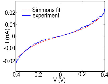
Figure 2(a) shows the current through the gap measured within V = ± 0.4 V (blue solid line). The width of the gap is estimated by fitting the tunnelling current to a Simmons model [13]. The current depends on the width of the gap w and the height of the tunnel barrier φ that depends on the work function of the conductor. The best fitting (red dashed line in Figure 2(b)) is obtained with φ = 0.92 eV and w ~ 1.95 nm.
Figure 2(b) shows the tunnelling curve versus V of the same device measured a few minutes after opening the gap (red line), after four weeks (blue line) and after seven weeks (green line). The sample was kept at room temperature and under vacuum during this period. Importantly, no significant change is observed in the current. The gap and the electrodes are thus stable at room temperature during long periods of time. Such behaviour is observed in around the 90% of the samples with variations in the current levels lower than 5%. The stability of the gap at room temperature thus allows characterization of the empty gap before molecular deposition.
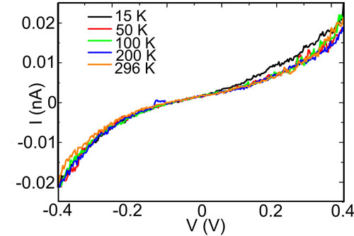
We have also measured the dependence of the current through the empty gap as a function of the temperature and the gate voltage. First, in Figure 3(a) we show I versus V measured at different temperatures covering the range from room temperature down to 15 K. The tunnelling current is independent of T in this range of temperatures. This is expected for a quantum process that is not thermally activated.
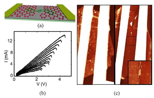
Figure 1. (a) Artist’s impression of a three-terminal device. FLG source and drain electrodes are separated by a nanometer-scale gap. The underlying silicon substrate is used as back-gate electrode; (b) Current-voltage characteristic of a feedback-controlled electroburning process; (c) AFM image (16 µm × 8 µm) showing a typical flake before (left) and after (right) the electroburning. The inset shows a zoom (2 µm × 2 µm) of the central part of the gap.
 (a)
(a)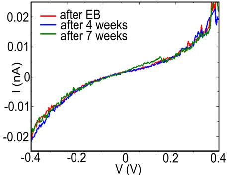 (b)
(b)
Figure 2. (a) Current versus bias measured for a particular FLG gap (blue solid line). The red dashed line is a fit to the Simmons model for tunnelling currents. Fitting parameters are: gap width: 1.95 nm, barrier height: 0.92 eV; (b) Current-voltage characteristic for the same FLG gap measured immediately after EB (red line), four weeks after EB (blue line) and seven weeks after EB (green line). The sample is kept in vacuum at room temperatures between each measurement. No significant change is observed in the current.
Further characterization explores the dependence of the tunnelling current with the gate voltage. Figure 3(b) shows the current as a function of Vg measured at a fixed V = 0.3 V. The current is independent of the gate voltage for all the measured bias and temperatures. Both aspects, temperature and gate independency of the current through the empty gap are of particular importance for molecular spintronics. It guarantees that any gate or temperature variation of the current originates from the properties of the molecule.
4. Statistics and Conclusions
We have electroburned 105 flakes in total. Of these flakes, 42 had an initial resistance lower than 500 Ω, 40 had a resistance between 500 and 1 kΩ. The remaining 23 had a resistance larger than 1 kΩ. After the electroburning process we classify the gaps in four groups depending on the shape of the characteristic I-V curve and the controllability of the electroburning. The first group, “tunnelling gaps”, includes the gaps showing the char-
 (a)
(a)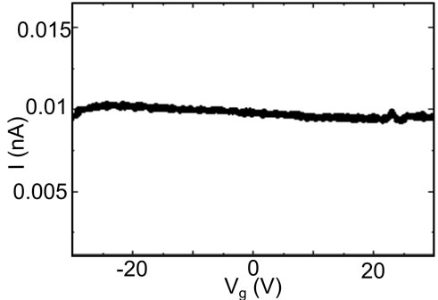 (b)
(b)
Figure 3. (a) Current versus bias measured at different temperatures from room temperature down to 15 K. No significant change is observed in the current; (b) Current versus gate voltage measured at a fixed V = 0.3 V between source and drain. No gate dependence is observed in the current.
acteristic tunnel shape (like the one plotted in Figure 2(a)) within a bias window lower than ±1.2 V. Above this voltage, the gap is not stable and reconnection of the electrodes occurs [14]. The second group, “larger gaps”, includes the gaps that were burned in a controlled step-wise decrease of the conductance but no current is observed within V = ±1.2 V. Due to the exponential decrease of the current with increasing gap width, this most likely implies a larger width than the samples in the first group; they may, however, still be suitable for molecular transport measurements (depending on the length of the molecule). In the third group, “abrupt breaking”, we include the devices in which the feedback was not fast enough during the electroburning. The conductance dropped abruptly to zero from resistance values lower than kΩ. Electroburning is not controlled in this case and therefore the final size of the gap may be larger than a few nanometres, not suitable for molecular linking. None of these gaps showed tunnelling current within the ±1.2 V bias window. Finally, a small percentage of the flakes do not break after several attempts. The reason is not clear but it could originate from impurities or irregularities during the fabrication process.
We have summarized the statistics in Table 1. The
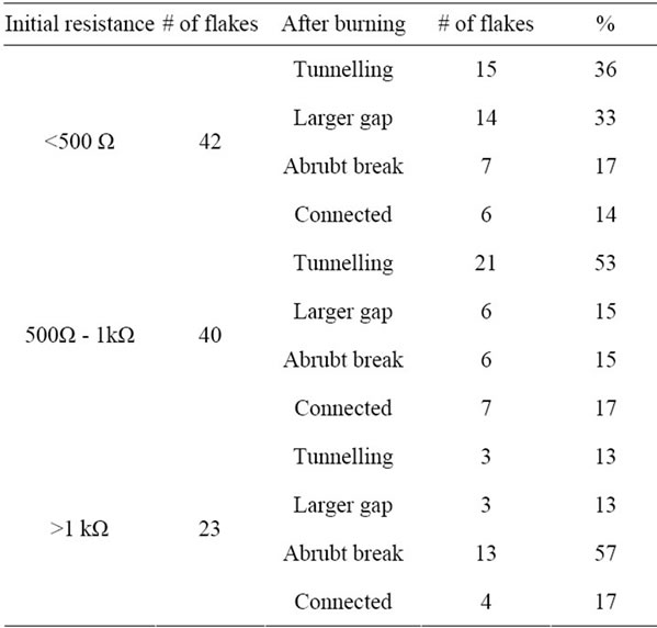
Table 1. Statistics of the relation between the initial resistance of the FLG flake and the final size of the gap.
four cases are separated in three groups depending on the initial resistance of the flakes. The table shows that the percentage of gaps still connected after successive electroburnings is around a 15 %, independent of the initial resistance. Interestingly, the percentage of gaps “broken” during the electromigration process is considerable larger (around 57 %) for flakes with initial resistances higher than 1 kΩ. In contrast, the number of gaps showing tunnelling curves or, at least, a controlled electroburning process is close to 70 % in flakes with initial resistances lower than 1 kΩ. Thicker flakes, with lower resistances, are therefore more suitable for the fabrication of nanometer-sized gaps.
To conclude, we have demonstrated that the tunnel current through the gap separating two graphene electrodes is independent of temperature and gate voltage. These properties together with the long-time stability (weeks) of the electrodes make FLG electrodes good candidates for molecular electronics at room temperatures and in ambient conditions. We conclude that the optimum flakes for the fabrication of nanometer-spaced graphene electrodes are those with initial resistances lower than 1 kΩ.
5. Acknowledgements
This work was supported by FOM and the EU FP7 program under the Grant Agreement ELFOS. We thank the students Nicolas Kramer and Joost Broersen.
REFERENCES
- A. H. Castro Neto, F. Guinea, N. M. R. Peres, K. S. Novoselov and A. K. Geim, “The Electronic Properties of Graphene,” Reviews of Modern Physics, Vol. 81, 2009, pp. 109-162. doi:10.1103/RevModPhys.81.109
- N. Tombros, C. Jozsa, M. Popinciuc, H. T. Jonkman and B. van Wees, “Electronic Transport and Spin Precession in Single Graphene Layers at Room Temperature,” Nature, Vol. 448, No. 7153, 2009, pp. 571-574. doi:10.1038/nature06037
- S. Cho, Y. F. Chen and M. S. Fuhrer, “Gate-Tunable Graphene Spin Valve,” Applied Physics Letters, Vol. 91, No. 12, 2007, Article ID: 123105. doi:10.1063/1.2784934
- S. Sanvito, “Molecular Spintronics,” Chemical Society Reviews, Vol. 40, No. 6, 2011, pp. 3336-3355. doi:10.1039/c1cs15047b
- F. Prins, A. J. Shaikh, J. H. van Esch, R. Eelkema and H. S. J. van der Zant, “Platinum-Nanogaps for Single-Molecule Electronics: Room-Temperature Stability,” Physical Chemistry Chemical Physics, Vol. 13, No. 32, 2011, pp. 14297-14301. doi:10.1039/c1cp20555b
- F. Elste and C. Timm, “Transport through Anisotropic Magnetic Molecules with Partially Ferromagnetic Leads: Spin-Charge Conversion and Negative Differential Conductance,” Physical Review B, Vol. 73, 2006, Article ID: 235305. doi:10.1103/PhysRevB.73.235305
- M. Misiorny and J. Barnas, “Magnetic Switching of a Single Molecular Magnet Due to Spin-Polarized Current,” Physical Review B, Vol. 75, No. 13, 2007, Article ID: 134425. doi:10.1103/PhysRevB.75.134425
- F. Prins, A. Barreiro, J. W. Ruitenberg, J. S. Seldenthuis, N. Aliaga-Alcalde, L. M. K. Vandersypen and H. S. J. van der Zant, “Room-Temperature Gating of Molecular Junctions Using Few-Layer Graphene Nanogap Electrodes” Nano Lettres, Vol. 11, No. 11, 2011, pp. 4607- 4611. doi:10.1021/nl202065x
- S. S. Datta, D. R. Strachan, E. J. Mele and A. T. C. Johnson, “Surface Potentials and Layer Charge Distributions in Few-Layer Graphene Films,” Nano Letters, Vol. 9, No. 1, 2008, pp. 7-11. doi:10.1021/nl8009044
- A. Castellanos-Gomez, R. H. M. Smit, N. Agraït, G. Rubio-Bollinger, “Spatially-Resolved Electronic Inhomogeneities of Graphene Due to Subsurface Charges,” Carbon, Vol. 50, No. 3, 2012, pp. 932-938. doi:10.1016/j.carbon.2011.09.055
- H. Park, A. K. L. Lim, A. P. Alivisatos, J. Park and P. L. McEuen, “Fabrication of Metallic Electrodes with Nanometer Separation by Electromigration,” Applied Physics Letters, Vol. 75, No. 2, 1999, p. 301. doi:10.1063/1.124354
- K. O’Neill, E. A. Osorio and H. S. J. van der Zant, “Self-Breaking in Planar Few-Atom Au Constrictions for Nanometer-Spaced Electrodes,” Applied Physics Letters, Vol. 90, No. 13, 2007, p. 133109. doi:10.1063/1.2716989
- J. G. Simmons, “Generalized Formula for the Electric Tunnel Effect between Similar Electrodes Separated by a Thin Insulating Film,” Journal of Applied Physics, Vol. 34, No. 6, 1963, p. 1793. doi:10.1063/1.1702682
- B. Standley, W. Z. Bao, H. Zhang, J. Bruck, C. N. Lau and M. Bockrath, “Graphene-Based Atomic-Scale Switches”, Nano Letters, Vol. 8, No. 10, 2008, p. 3345. doi:10.1021/nl801774a