Open Journal of Synthesis Theory and Applications
Vol. 2 No. 1 (2013) , Article ID: 27197 , 5 pages DOI:10.4236/ojsta.2013.21003
Synthesis and Characterization of CuIn2n+1S3n+2 (with n = 0, 1, 2, 3 and 5) Powders
Photovoltaic and Semiconductor Materials Laboratory, Tunis-El Manar University, Tunis, Tunisia
Email: *naoufel_khemiri@yahoo.fr
Received November 25, 2012; revised December 28, 2012; accepted January 5, 2013
Keywords: CuIn2n+1S3n+2; Synthesis; Structural Properties
ABSTRACT
CuIn2n+1S3n+2 crystals were synthesized by horizontal Bridgman method using high purity copper, indium, sulfur elements. The phases and crystallographic structure of the CuIn2n+1S3n+2 crystals were analyzed by X-ray diffraction (XRD) and the composition of the material powders was determined using the energy dispersive X-ray analysis (EDX). Measurement data revealed that CuIn2n+1S3n+2 materials have not the same structure. In fact, CuInS2 and CuIn3S5 crystallize in the chalcopyrite structure whereas CuIn5S8, CuIn7S11 and CuIn11S17 crystallize in the cubic spinel structure.
1. Introduction
Developments of thin film solar cells based on CuInS2 and related alloys have made considerable progress in recent years. Copper indium sulfide thin films are one of the most promising absorber materials in solar cells because he has a high optical absorption coefficient (105 cm−1), and an optical band gap of 1.5 eV [1] and that’s why CuIn2n+1S3n+2 materials attract much attention. In addition, the materials do not contain any toxic elements such as Ga or Se, and this may have an advantage in comparison with other ternary materials like CuIn2n+1Se3n+2 and CuGa2n+1S3n+2. They belong to I-III2n+1-VI3n+2 ternary materials which are receiving a great deal of attention as candidate materials for visible-light and IR emitters, high-efficiency solar cells, and other semiconductor and quantum-electronic devices [2]. Many researchers tried to synthesize CuInS2 material by various methods because of its important properties, a new green synthesis is described by some authors without using any organic solvent [3], a new strategy has been presented to the controllable synthesis of CuInS2 hollow nanospheres based on the Cu2O solid nanospheres as the precursor in the absence of any surfactant [4], a facile and low-cost method was developed to prepare metastable wurtzite copper indium sulfide (CuInS2) nanocrystals under atmospheric conditions [5] and luminescent CuInS2 nanocrystals were synthesized in dodecanethiol precursors [6]. I-III2n+1-VI3n+2 ternary materials are called ordered vacancy compound (OVC). The formation of the OVC compound CuIn3Se5 has already been explained as due to the presence of a single pair of the defect complex (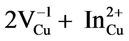 ) in every five units of CIS [7]. In the present study, we have investigated the structural properties of CuIn2n+1S3n+2 powders synthesized by the horizontal Bridgman method.
2. CuIn2n+1S3n+2 Materials
In order to understand the formation of ternary compounds with chemical formula CuIn2n+1S3n+2, their phase equilibrate can be discussed in terms of temperature or composition. These compounds stabilize due to the ordering of the neutral defect pairs ( ) in the CuInS2 phase and this is due to its huge tolerance to off-stoichiometry [8]. In our knowledge, few papers [9] dealing with the physical properties of CuIn2n+1S3n+2 compounds have been reported but not much is known about the fundamental properties of this system. The ternary compositional triangle is the basis for analyzing the composition phase behavior of these materials. In Figure 1, a schematic ternary diagram for CuIn2n+1S3n+2 compounds is shown. This ternary diagram can be reduced in a pseudo-binary diagram along the interconnection line between Cu2S and In2S3 binary materials. Indeed, by combining these two compounds, we can obtain all materials belonging to the family with chemical formula CuIn2n+1S3n+2 with n = 0, 1, 2, 3 and 5. The bold points along the line connecting Cu2S and In2S3 represent these materials.
3. Synthesis of Materials
The CuIn2n+1S3n+2 (with n = 0, 1, 2, 3 and 5) crystals have
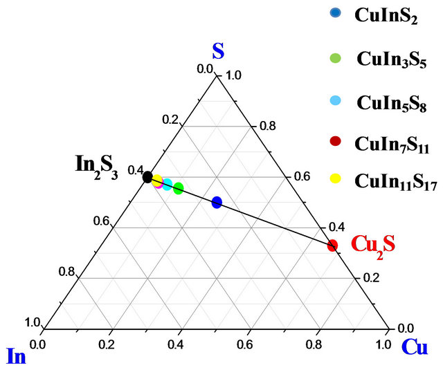
Figure 1. The ternary system Cu-In-S including the pseudo-binary section Cu2S-In2S3.
been prepared by Bridgman horizontal method growth. High purity elemental materials of copper, indium and sulfur (Balzers 99.999%) were taken in proportions corresponding to the stoichiometric composition of the compounds CuInS2, CuIn3S5, CuIn5S8, CuIn7S11 and CuIn11S17 and then loaded into five quartz ampoules. The growth of crystals was carried out in ampoules (20 cm in length with thickness 2 mm), that were pre-cleaned by chemical etching in concentrated acid HF, washed in distilled water then with acetone, and finally, dried in oven at 150˚C during 30 minutes. The ampoules were evacuated down to 10−5 mbar and were sealed off. The sealed ampoules containing the pure elements were placed into a horizontal position in programmable furnace (Nabertherm-Allemagne). For the synthesis, the temperature of the furnace was increased from room temperature to 600˚C with a slow rate of 10˚C/hour in order to avoid explosions due to sulfur vapor pressure (2 atm at 493˚C and 10 atm at 640˚C). The temperature was kept constant at 600˚C for 24 hours. Then, the temperature was increased with a rate of 20˚C/hour up to 1000˚C. A complete homogenization could be obtained by keeping the melt at 1000˚C for 48 hours. After that, the temperature was lowered to 800˚C at a rate of 10˚C/hour and the furnace was switched off until the tube reached room temperature. Then, the ampoules were removed from the furnace and were broken to retrieve the synthesized ingots. The resulting ingots are opaque and black in color. Figure 2 represents the CuIn11S17 ingot. Finally, the CuIn2n+1S3n+2 ingots were crushed in order to obtain CuIn2n+1S3n+2 powders. The phases and crystallographic structure of the CuIn2n+1S3n+2 powders were investigated by X-ray diffraction (XRD) using monochromatic CuKα (λ = 1.54052 Å) radiation in 2θ range of 20˚ - 60˚. The operation voltage and current used are, respectively, 40 kV and 30 mA. The observed phases were determined by

Figure 2. Photographs showing the CuIn11S17 ingot.
comparing the d-spacing with Joint Committee on Powder Diffraction Standard (JCPDS) data files. The composition of powders was determined by means of energy dispersive X-ray analysis (EDX) by a JEOL 6700F equipment which uses K-ray for Cu and L-ray for In and S as standards.
4. Structural Characterization
4.1. XRD Results
X-ray diffraction (XRD) was used to study the structural properties of CuInS2, CuIn3S5, CuIn5S8, CuIn7S11 and CuIn11S17 powders. Figure 3 shows the X-ray diffraction (XRD) patterns of the CuIn2n+1S3n+2 materials (with n = 0, 1, 2, 3 and 5). It is clear from Figures 3(a), (b) that the peak due to the 112 plane has the highest intensity for the CuInS2 (PDF 27-0159) and CuIn3S5 (PDF 35-1349) powders while the highest intensity for CuIn5S8 (PDF 72-0956), CuIn7S11 (PDF 49-1383) and CuIn11S17 (PDF 34-0797) powders is the peak due to the 311 plane. All the diffraction peaks of the patterns shown in Figure 3 could be indexed as those of CuIn2n+1S3n+2 (n = 0, 1, 2, 3 and 5) with tetragonal chalcopyrite structure for CuInS2 (space group I-42d [10]) and CuIn3S5 (space group P-42c [11]) and with cubic spinel structure (space group Fd3m [12-14]) for CuIn5S8, CuIn7S11 and CuIn11S17. This transition in the crystal structure between n = 0 and 1 and n = 2, 3 and 5 in the CuIn2n+1S3n+2 system can be explained by the migration of a part of In3+ ions towards octahedral sites when the indium atoms increase in the structure. Indeed, the In3+ ions can be stabilized in both tetrahedral and octahedral sites but tend to form bonding with octahedral coordinations. The spinel structure is favored by increasing the indium content in the CuIn2n+1S3n+2 system [15]. We also note that the XRD patterns of all compounds do not contain extra reflections corresponding to the elements or other secondary phases, which confirms the homogeneity of the synthesized materials. The lattice parameters (a) and (c) of CuInS2 and CuIn3S5 was calculated by using Equation (1) whereas Equation (2) was used to calculate the lattice parameter (a) of CuIn5S8, CuIn7S11 and CuIn11S17 [16].
 (1)
(1)
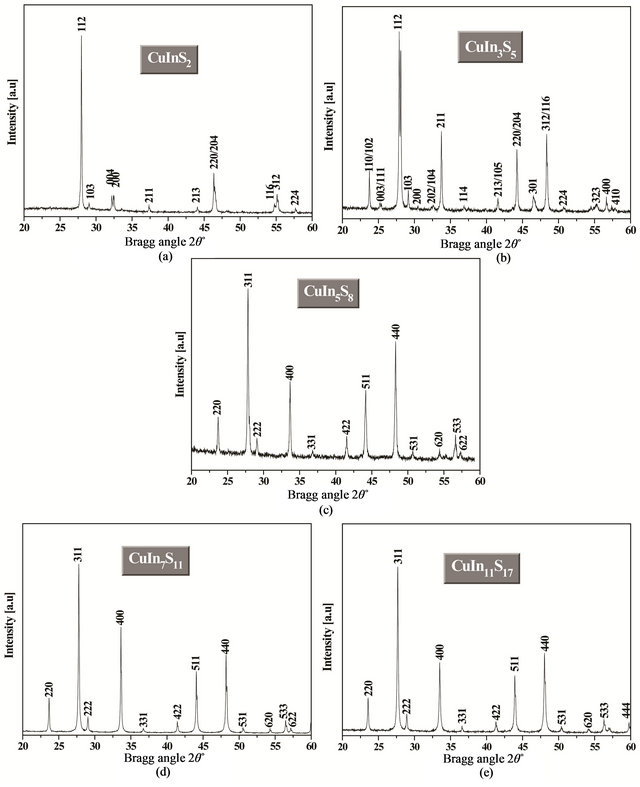
Figure 3. XRD patterns of the synthesized: (a) CuInS2 (b) CuIn3S5 (c) CuIn5S8 (d) CuIn7S11 and (e) CuIn11S17 powders.
 (2)
(2)
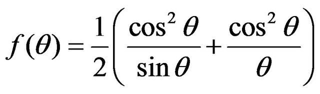
where d is interplanar spacing determined using Bragg’s equation and h, k, l are the miller indices of the lattice planes. The corrected values of lattice parameters are estimated from Nelson-Riley [17] method. Consequently, Nelson-Riley function [18]:
 (3)
(3)
(where θ is Bragg angle) is calculated and the Nelson-Riley plot is represented for different reflections. In this method, the value of lattice parameter is determined by extrapolating Nelson-Riley functions to f(θ) → 0.
Figure 4 represents the Nelson-Riley plots for CuInS2 and CuIn7S11 powders. The calculated values of lattice parameters were collected in Table 1.
4.2. EDX Results
The atomic ratios of Cu, In and S elements and the chemical composition of the prepared powders have been determined using the energy dispersive X-ray analysis (EDX). The EDX analysis is made at several zones of the powders in order to obtain an average atomic concentration. The atomic ratios of the elements and the composition of powders are presented in Table 2. The uncertainty of the present measurements is about 5%. As is seen in Table 2, the compositions of CuIn2n+1S3n+2 (n = 0, 1, 2, 3 and 5) powders is fairly close to the ideal theoretical values of the starting composition. We also note that all powders were deficient in sulfur.
5. Conclusion
In summary, CuIn2n+1S3n+2 (n = 0, 1, 2, 3 and 5) materials were successfully synthesized using the horizontal Bridgman method. The XRD spectra of the powders indicate that the CuIn2n+1S3n+2 powders can be formed in different structures. Indeed, for n = 0 and 1, the powders crystallize in the chalcopyrite structure with the preferential orientation along 112 plane. On the passage to n = 2, 3 and 5, CuIn5S8, CuIn7S11 and CuIn11S17 powders crystallize in the spinel structure with the preferential orientation along 311 plane. The compositions of CuIn2n+1S3n+2

Lattice parameters (Å)
Figure 4. Nelson-Riley plots for calculation of corrected lattice parameters of CuInS2 and CuIn7S11 powders.
Table 1. Lattice parameters of CuIn2n+1S3n+2 (n = 0, 1, 2, 3 and 5) powders.

Table 2. Chemical compositions of CuIn2n+1S3n+2 (n = 0, 1, 2, 3 and 5) powders.

powders were verified by EDX measurements and all powders are deficient in sulfur.
REFERENCES
- Y. Peña, S. Lugo, M. Calixto-Rodriguez, A. Vázquez, I. Gómez and P. Elizondo, “CuInS2 Thin Films Obtained through the Annealing of Chemically Deposited In2S3-CuS Thin Films,” Applied Surface Science, Vol. 257, No. 6, 2011, pp. 2193-2196. doi:10.1016/j.apsusc.2010.09.071
- I. V. Bodnar, “Growth, Transmission Spectra, and Thermal Expansion of CuGa3Se5 Single Crystals,” Inorganic Materials, Vol. 44, No. 2, 2008, pp. 104-109. doi:10.1134/S0020168508020040
- F. Bensebaa, C. Durand and A. Aouadou, “A New Green Synthesis Method of CuInS2 and CuInSe2 Nanoparticles and Their Integration into Thin Films,” Journal of Nanoparticle Research, Vol. 12, No. 5, 2010, pp. 1897-1903. doi:10.1007/s11051-009-9752-5
- W. Zhang, H. Zeng, Z. Yang and Q. Wang, “New Strategy to the Controllable Synthesis of CuInS2 Hollow Nanospheres and Their Applications in Lithium Ion Batteries,” Journal of Solid State Chemistry, Vol. 186, 2012, pp. 58-63. doi:10.1016/j.jssc.2011.11.042
- J. Guo, W. H. Zhou, M. Li, Z. L. Hou, J. Jiao, Z. J. Zhou and S. X. Wu, “Synthesis of Bullet-Like Wurtzite CuInS2 Nanocrystals under Atmospheric Conditions,” Journal of Crystal Growth, Vol. 359, 2012, pp. 72-76. doi:10.1016/j.jcrysgro.2012.08.029
- D. Li, Y. Zou and D. Yang, “Controlled Synthesis of Luminescent CuInS2 Nanocrystals and Their Optical Properties,” Journal of Luminescence, Vol. 132, No. 2, 2012, pp. 313-317. doi:10.1016/j.jlumin.2011.08.030
- R. R. Philip, S. Dhanya, T. N. Ashokan and B. Pradeep, “Effect of Ga Incorporation on Valence Band Splitting of OVC CuIn3Se5 Thin Films,” Journal of Physics and Chemistry of Solids, Vol. 72, No. 4, 2011, pp. 294-29. doi:10.1016/j.jpcs.2011.01.011
- B. Berenguier and H. J. Lewerenz, “Efficient Solar Energy Conversion with Electrochemically Conditioned CuInS2 Thin Film Absorber Layers,” Electrochemistry Communications, Vol. 8, No. 1, 2006, pp. 165-169. doi:10.1016/j.elecom.2005.08.012
- I. V. Bodnar, V. A. Polubok, V. Y. Rud and M. S. Serginov, “Structure Based on Silicon Compounds Cu(Ag)InnSm,” Physics and Semiconductors Technique, Vol. 38, No. 2, 2004, pp. 202-206.
- S. H. Chaki and A. Agarwal, “Growth, Surface Microtopographic and Thermal Studies of CuInS2,” Journal of Crystal Growth, Vol. 308, No. 1, 2007, pp. 176-179.
- N. Khemiri and M. Kanzari, “Comparative Study of Structural and Morphological Properties of CuIn3S5 and CuIn7S11 Materials,” Nuclear Instruments and Methods in Physics Research B, Vol. 268, No. 3-4, 2010, pp. 268-272. doi:10.1016/j.nimb.2009.10.175
- A. F. Qasrawi and N. M. Gasanly, “Crystal Data, Photoconductivity and Carrier Mechanisms in CuIn5S8 Single Crystals,” Crystal Research and Technology, Vol. 36, No. 12, 2001, pp. 1399-1410. doi:10.1002/1521-4079(200112)36:12<1399::AID-CRAT1399>3.0.CO;2-O
- F. Py, M. Womes, J. M. Durand, J. Olivier-Fourcade, J. C. Jumas, J. M. Esteva and R. C. Karnatak, “Copper in In2S3: A Study by X-Ray Diffraction, Diffuse Reflectance and X-Ray Absorption,” Journal of Alloys and Compounds, Vol. 178, No. 1-2, 1992, pp. 297-304. doi:10.1016/0925-8388(92)90271-A
- K. Basavaswaran, T. Sugiura, Y. Ueno and H. Minoura, “Preparation of Polycrystalline CuIn11S17 Semiconductor with High Crystallinity and Its Preparation of Polycrystalline CuIn11S17 Semiconductor with High Crystallinity and Its Characterization,” Journal of Materials Science Letters, Vol. 9, No. 12, 1990, pp. 1448-1452. doi:10.1007/BF00721612
- N. Khemiri and M. Kanzari, “A Comparative Study of the Properties of Thermally Evaporated CuIn2n+1S3n+2 (n = 0, 1, 2 and 3) Thin Films,” Thin Solid Films, Vol. 519, No. 21, 2011, pp. 7201-7206. doi:10.1016/j.tsf.2010.12.212
- M. Ladd and R. Palmer, “Structure Determination by X-Ray Cristallography,” Plenum Publishers, New York, 2003. doi:10.1007/978-1-4615-0101-5
- B. D. Cullity, “Elements of X-Ray Diffraction,” Addison-Wesley, Boston, 1979.
- G. I. Rusu, P. Prepelita, R. S. Rusu, N. Apetroaie, G. Oniciuc and A. Amarie, “On the Structural and Optical Characteristics of Zinc Telluride Thin Films,” Journal of Optoelectronics and Advanced Materials, Vol. 8, No. 3, pp. 922-926.
NOTES
*Corresponding author.