Advances in Materials Physics and Chemistry
Vol.07 No.02(2017), Article ID:74252,16 pages
10.4236/ampc.2017.72005
Characterization and Structural Property of Indium Tin Oxide Thin Films
Ehsan Parsianpour*, Davood Raoufi, Mojtaba Roostaei, Bahram Sohrabi, Feridoun Samavat
Physics Department, Bu-Ali Sina University, Hamedan, Iran

Copyright © 2017 by authors and Scientific Research Publishing Inc.
This work is licensed under the Creative Commons Attribution-NonCommercial International License (CC BY-NC 4.0).
http://creativecommons.org/licenses/by-nc/4.0/


Received: December 3, 2016; Accepted: February 17, 2017; Published: February 20, 2017
ABSTRACT
In this study, Indium Tin Oxide (ITO) thin films were deposited by electron beam evaporation on white glass substrates with thicknesses of about 50, 100 and 170 nm. We investigated structural properties by X-ray Diffraction (XRD) and X-ray reflectivity (XRR). The results showed that ITO thin films have a crystalline structure with a domain that increases in size with increasing thickness. For uniform electron density, as the thin film roughness increases, reflectivity curve slope also increases. Also thinner film has more fringes than thicker film. The roughness determines how quickly the reflected signal decays. XRR technique is more suitable for very thin films, approximately 20 nm and less.
Keywords:
ITO, Thin Film, X-Ray Reflectivity

1. Introduction
Indium oxide doped with tin (In2O3 90%: SnO2 10%) is briefly called ITO that is from the most famous transparent conductive oxides. Grown layers’ completeness depends on the quality of interfaces which in turn depend on numbers of properties such as crystal structure and defects existence in thin film. In order to optimize above characteristics such as high transparency and low electrical resistance parameters such as thickness, doping type and level, and other conditions should be optimized deposited [1] - [6] . ITO has been specified optical property of conductive oxides such as In2O3 that heavily depends on caused imperfect density by external doping or their growth conditions. Originally, the addition of fluorine and tin atoms has been reported for external doping [7] . ITO films have played an important role in deciding their characteristics and achieving highly crystalline and morphologically uniform thin films on flexible or suitable substrates for two applications [8] [9] . Also ITO thin films find different applications in optoelectronic system, for example, organic light-emitting diodes (OLEDs) [7] [10] [11] , transparent electrodes, transparent heating elements, coating electrodes in optoelectronics instruments (flat panel displays (FPDs)), photovoltaic cells, charge-coupled tools, electro-luminescence instruments [12] [13] [14] , photo-diodes [15] [16] [17] , windows with energy efficient, electro chromic instruments, liquid crystal displays (LCDs) [18] , image sensors [19] [20] , solar cells [21] - [28] , gas sensors, photo crystal and photo electro crystal and heat reflector mirrors [29] [30] [31] . ITO thin films can be produced by different deposition techniques such as direct current (DC) and radio frequency (RF) magnetron sputtering although a variety of production methods have been used for making ITO films [32] - [41] , for example electron beam evaporation [42] [43] [44] , chemical vapor deposition [45] [46] , spray pyrolysis [47] [48] and reactive thermal evaporation [49] . One of the techniques, important for studying physical and structural feature of thin films is X-ray reflectivity (XRR). Also XRR is a highly efficient technique to research the structure of thin films from atomic scales to micrometer to obtain interface structures of thin film, density, thickness, and interfacial roughness. In the other word, the roughness of an interface is considered as a very important parameter in many industrial applications and quality of interfaces estimated by that [50] [51] . The ITO has proven to be an advanced semiconducting material opening a new window in many electronic and optical industries due to its large optical band gap and the plasma frequency lying in the near IR spectral region [52] . Spray pyrolysis technique offers a simple and inexpensive experimental arrangement, ease of adding various doping materials, high growth rate and mass production capability for uniform large- area coatings which are desirable for industrial applications [53] [54] [55] . Although the dominant commercial market for laser glass is in large laser systems for inertial confinement fusion research with application to fusion energy and weapons physics science [56] , these materials have also found their way into a number of industrial and laboratory environments. For example, one leading application is in the field of laser shock peening [57] . Structural characteristics of thin films are technologically very important. Characteristics of these films are necessary to design the films with required physical properties. Grazing incidence X-ray reflectivity (GIXR) technique is becoming popular for structural characteristics of thin inorganic and organic films. This is a non-destructive tool for structural characteristics of thin films and multi-layer structures. In GIXR technique, the X-ray beam is incident on the sample at a grazing angle and the interfered reflected beam is collected by an X-ray counter. The interference occurs due to the presence of interfaces in the sample. The interference periods depend on the thickness of the layers and the amplitude of the interference oscillations depends on the contrast of the electron density between the layers and the interfacial roughness. Thus, the GIXR data contain structural information about the film such as thickness, density and roughness of the film and its individual layers [58] - [64] . This study focuses on structural properties of ITO thin films deposited by electron beam evaporation technique.
2. Materials and Methods
In this study, due to high melting point of Indium Tin Oxide (ITO; SnO2, In2O3, Merck), the electron beam evaporation method instead of thermal evaporation technique was used. Indium Tin Oxide (weight ratio; 90% In2O3 and 10% SnO2) was used as the evaporation source. Before the exposure of substrates in the vacuum chamber, they were immersed in an acid bath and hydrogen peroxide for 20 minutes, and then cleaned in pure acetone for 5 minutes. Finally, they were washed with distilled water and then dried. In order to ensure about the absence of lipid, the substrates were ultrasonically defeated in bath of alcohol Ethy- lic. After installing the substrates in the vacuum chamber of deposition, the initial pressure was adjusted to 1 × 10⁻⁶ mbar. Then by flowing of inert gas the substrate surface was bombarded. The cleaning process of substrate was performed to improve the substrate adhesion and prevent contamination of layers. Control of the partial pressure of the oxygen (purity 99.99%) was regulated in stable amount 6.2 × 10⁻⁵ mbar. The film deposition was carried out in deposition rate 0.10 nm・s−1 to produce thin films with thicknesses of about 50, 100 and 170 nm. Film thicknesses were measured with a quartz crystal microbalance. The substrate temperature, during the film deposition, was kept constant at 400˚C for 1 h.
Characterization
Structures of ITO thin films were studied using X-ray diffraction (XRD; Philips Powder Diffractometer type PW 1373 goniometer) and X-ray reflectivity (XRR; XPERT-PRO reflectometer). The X-ray wavelength was 1.5405 Å and the diffraction patterns were recorded over the 2θ range 20˚ - 70˚ with a scanning speed of 0.04˚ min−1 for all thin films. The XRR diffraction patterns were recorded over the 2θ range 0˚ - 4˚ with a scanning speed of 0.002˚ min−1 for thin films with nominal thicknesses of 50 and 100 nm and a scanning speed of 0.001˚ min−1 for thin film with thickness of 170 nm.
3. Results and Discussions
3.1. XRD Characterization
The structural studies of the ITO thin films were carried out using X-ray diffraction. Figure 1 shows the X-ray diffraction pattern of ITO thin film, clearly demonstrating a crystalline structure.
The most useful information to be extracted by the XRD method is a grain size calculation, using the peak width at half height. Peak width at half height depends on the number of coherent reflector plates the crystalline structure. Using the Scherrer equation, the crystalline domain size (which can be equal to or smaller than the grain size) can be calculated from measurement of the width of the observed X-ray diffraction peaks:
 (1)
(1)
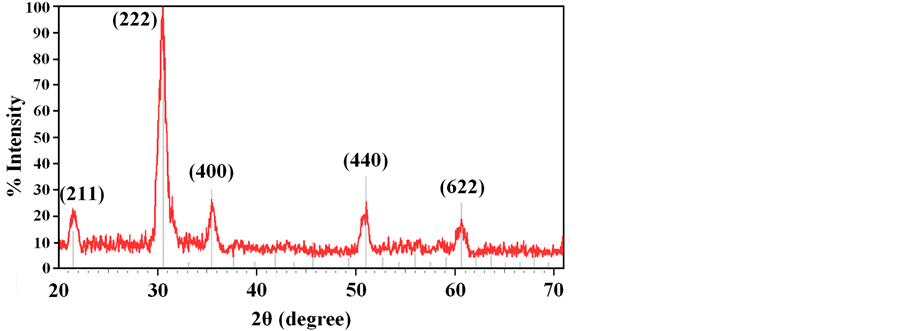
Figure 1. X-ray diffraction pattern of ITO thin film with deposition rate 0.10 nm・s−1 and In2O3 spectra peaks.
In which the D represents crystalline domain size (nm), λ is the wavelength of the X-ray probe beam (0.15405 nm), B is the peak width at half height (phase peak) in terms of radians, K is the shape factor (approximately 0.94) and θ is the diffraction angle. Tables 1-3 present the values of K and λ are constant and determinate for each of 5 standard major peaks. Also B and θ values were obtained by the use of XPowderProVer.2010.01.30 software. The results of analysis material by X-ray diffraction are shown in Figure 1, which can be indexed as the primitive cubic system by comparison with data from ITO (JCPDS No. 06-0416) [65] . The diffraction peaks at 2θ = 21.88˚, 30.84˚, 35.81˚, 51.32˚, 60.96˚, correspond to (211), (222), (400), (440) and (622) planes respectively. The average size of nanoparticles 20 to 34 nm was obtained. X ray diffraction pattern of thin films 50, 100 and 170 nm is shown in Figure 2. The results show decreasing X-ray diffraction peak widths with increasing thickness, corresponding to more regular crystalline structure of the material and reduced structural.
3.2. XRR Analyses
3.2.1. X-Ray Interaction with Matter
The material index of refraction in the X-ray region can be written as:
 (2)
(2)
where , here λ is the X-ray wavelength (λ = 1.54 Å),
  is the classical electron radius or Thompson scattering length (2.82 × 10⁻⁵ Å),
  is effective electron density and
 , where µ is the X-ray absorption length. Since the X-ray wavelength is comparable with atomic dimensions and the roughness of thin film surface, X-ray specular reflection can be described by Fresnel laws of classical optics. XRR critical angle
 (3)
(3)
Equation (2) is resulting the evaluation of Snell’s law for small angles  [67] . The critical angle for a layer is a function of its electron density, if one is known, the other can be determined using XRR. Figure 3 shows, the

Table 1. Characteristics of ITO thin film at thickness 50 nm.
Table 2. Characteristics of ITO thin film at thickness 100 nm.
Table 3. Characteristics of ITO thin film at thickness 170 nm.
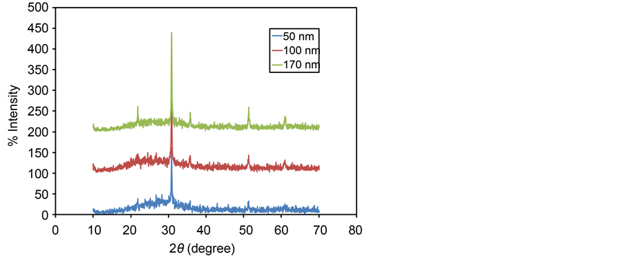
Figure 2. X-ray diffraction pattern of ITO thin films with deposition rate 0.10 nm∙s−1 for thicknesses of 50, 100 and 170 nm.
experimental data of ITO thin films with nominal thicknesses of 50, 100 and 170 nm. The critical angles directly were obtained from XRR logarithmic curve. Then, the mean electron density (MED) of thin films was obtained from Equation (2) (Table 4).
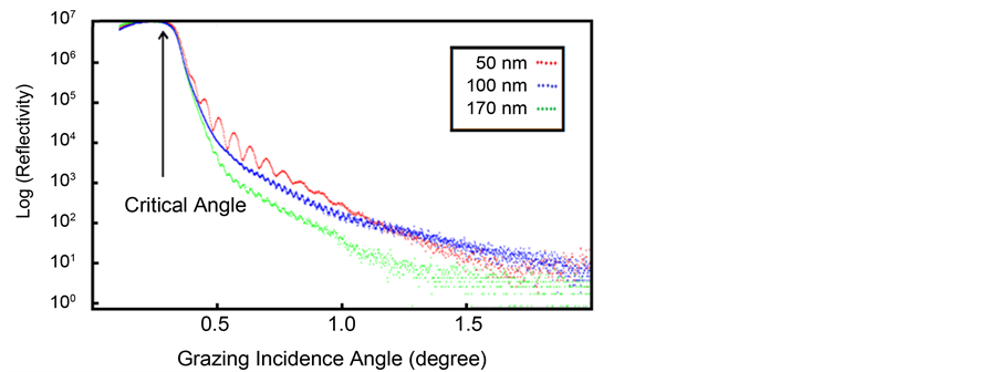
Figure 3. XRR data of ITO thin films in different thicknesses.
Table 4. Calculated structural parameters of ITO thin films for thicknesses 50, 100 and 170 nm.
By the way, up proceedings were not carried out for thin film 250 nm due to the detection absence of Kiessig fringes. The following equation describes refraction coefficient n. Materials scattering property is with electron density ρ and scattering amplitude  for each electron.
 (4)
(4)
where  and radiation wavelength
  depends on wave vector k. Elec-
tron density  is in order
  in condensed material. In other word, with
r0 = 2.82 × 10⁻⁵ Å and k approximately 4 Å−1,  is in order
  and less than 1 that it describe the refraction phenomenon is visible in range X ray weakly. Snell’s law with small angles
  and
and  is according to equation
 . The critical angle is
  for external general reflection with control
  and with expansion to cosines:
 (5)
(5)
By using up parameter magnitudes,  is in order 1 m radian. Vertical axis shows reflected X-ray intensity from the surface and interfacial layers measured by the detector, according to the angle 2θ (Figure 3 and Figure 4). The first noted notice that attracts attention is Kiessig fringes absence of thin film of 250 nanometers. Thus, XRR technique is more suitable for thin film of less than 100 nm and preferably will have very good results for ultra-thin films (less than 20 nm) [58] .
Figure 5 and Figure 6 have been shown schematic of film structure information and detector from film surface with X-ray reflectivity technique. The point
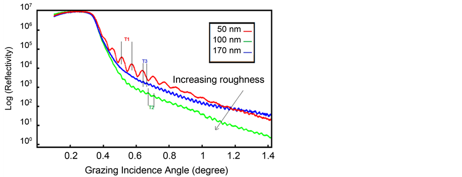
Figure 4. Simulated curve of ITO thin films in different thicknesses.
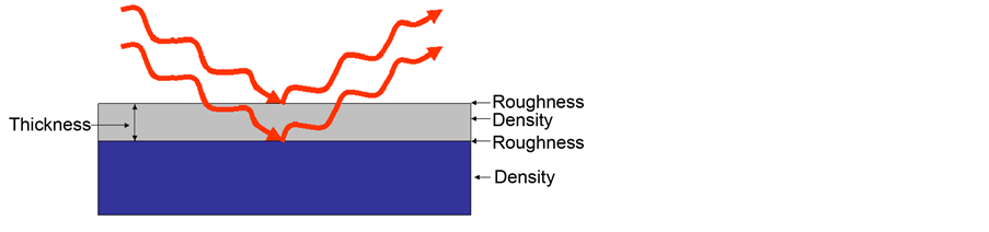
Figure 5. Thin film structure information with X-ray reflectivity technique.

Figure 6. Schematic of X-ray reflectivity detector from thin film surface.
in Figure 4 is critical angle adjustment of films that it illustrates the same quality of films in the crystal structure and conditions of film deposition. In the other word, the films are relatively uniform electron density (Equations (4) and (5)). In early look at the curves; difference in the Kiessig fringes is obvious for each sample. According to Equations (4), (5) and with known critical angle, they are calculated electron density, refraction coefficient and film thickness according to Kiessig fringes of X-ray reflectivity curves. Also reflectivity curve slope is the same roughness of thin film surface. Reflectivity curve slope increases with the increasing of thin film roughness [68] [69] .
3.2.2. Roughness and Thickness
Generally, there are three ways to data analyses of X-ray reflectivity for thin films:
1) The model of dynamic scattering by using of recursive formula.
2) The model of Distorted Wave Born Approximate (DWBA).
3) The model of reverse furrier transform by Born Approximate (BA).
In present work, the GENX software by DWBA was used to data analyses and real thickness of films, also Simulation and fitting X-ray reflectivity data and data analysis were carried out using MATLAB software by curve fitting tool (smooth) that simulated curves are shown in Figure 6. The Kiessig fringes result from constructive and destructive interference of X rays reflected from the two interfaces as a consequence of the angular-dependent phase shift. Their period is determined by the thickness of the layer. The film thickness is the same distance two consecutive peaks incurve and it has reverse relation with its magnitude. In the other word, thinner film has more fringes than thicker film (Figure 6).
To measure the thickness, according to Snell’s law for two consecutive peaks of the reflectivity curves:
 (6)
(6)
where, d is the thickness of film. Due to the small angle approximation for Snell’s law , we have used:
 (7)
(7)
Therefore, the thickness of each film is obtained (Table 4). Interference fringes are created by the phase difference between X-rays reflected from different surfaces. Roughness determines how quickly the reflected signal decays. A rougher surface produces more diffuse scatter, causing the reflected beam intensity to decay more with Theta (Figure 6). The roughness of each thin film was calculated as shown in Table 4 [68] .
3.2.3. Optical Theory
The optical absorption coefficient, α is obtained using the optical absorbance A from , d is the film thickness and A was obtained from the equation
 ,
,  and I are the primary and secondary intensity of beams, respectively. The film energy gap
 , is calculated using the formula from Davis and Mott
  that for direct transition n = 2 and for an indirect transition n = 0.5, hν is the input photon energy and B is given by
 ,
,  is the extrapolated dc conductivity at T = 0 K, c is the light speed, Eₑ is the extent of the band tailing and nb is the refractive index of the material [70] [71] [72] [73] [74] [75] . Also for the amorphous materials in the high absorption region
 , α can be described using the Davis and Mott formula, if the multiple reflections are neglected, the transmittance, T of the film is given by:
 (8)
(8)
R is the reflectance that can be determined from measurements of both A and T using above equation, which can be rewritten in the following form:
 (9)
(9)
The reflectance R of the material of refractive index, n and extinction coefficient, k is given by:
 (10)
(10)
The absorption coefficient α is related to k by:
 (11)
(11)
where λ is the wavelength. Using above equations the values of R, n, and k are calculated, respectively.
But, if the absorption edge in numerous amorphous materials in the low absorption region , follows the Urbach rule given by [73] [76] :
 (12)
(12)
where hν is the photon energy and  is the terminative width of localized situations in the band causing from absence of long-range order (wonky depending on temperature) [77] . For optimizing the optical and physical properties of nanomaterials, the most important parameter to control is the interfacial system free energy of the system (solution) [78] . Whit Gibb’s adsorption equation
  that
that  is the chemical potential of the adsorbed species and y is
the superficial adsorption density.  where G is Gibb’s free energy and
 is the amount of substance of the component or specie i. Using Gibb’s adsorption equation, the variation of water oxide surface (interfacial) tension with ionic strength (I) maximum surface charge density
 , and pH has been developed from Gibbs adsorption equation.
It is given as

 , y, I is given in respectively
 ,
,  ,
,  and
and  means interfa-
cial tension at equilibrium [78] . The size of the nanoparticles is directly related to the conditions for nucleation that include pH, ionic strength and concentration of precursors. Solid phases (particles, crystals thin films) evolve from solutions through nucleation and growth processes. The total change in free energy
of the system is given as ,
,  is the
chemical component while  is the surface component
  is the free energy per unit volume. With assume that the new phase is there-fore and
spherical has a volume of .
.  is the surface component of the free energy due to surface tension
  where θ is the
wetting angle  differentiates the expression for change in free energy of the system from that of homogeneous nucleation [78] [79] .
3.2.4. Suggestions
Using of X-ray reflectivity technique for various thin films study and investigation, the films should be very thin (approximately 20 nm and less).
4. Conclusion
In this work, ITO thin films were deposited by electron beam evaporation on white glass substrates with thicknesses of about 50, 100 and 170 nm. Using XRD and XRR, as the thickness were increased; the changes in structural properties of the ITO thin films were investigated. The results showed that ITO thin films maintained the crystalline structure and they had crystalline structure with a do- main that increased in size with increasing thickness. The distance between the Kiessig fringes is inversely proportional to the thickness of film. Hence, thicker films have smaller fringes compared with thinner films. The films with relatively uniform electron density, with increased reflectivity curve slope, increase thin film roughness. Roughness determines how quickly the reflected signal decays. Performed proceedings for each three thin films were not carried out for thin film 250 nm due to the detection absence of Kiessig fringes. Thus, XRR technique is more suitable for thin film of less than 100 nm and preferably will have very good results for ultra-thin films (less than 20 nm).
Acknowledgements
We would like to acknowledge KEFA Company (Iran, Tehran) that has supported us by providing X-ray reflectivity of thin films.
Cite this paper
Parsianpour, E., Raoufi, D., Roostaei, M., Sohrabi, B. and Samavat, F. (2017) Characterization and Structural Property of Indium Tin Oxide Thin Films. Advances in Materials Physics and Chemistry, 7, 42-57. https://doi.org/10.4236/ampc.2017.72005
References
- 1. Islam, S., Saklayen, G., Rahman, F., Baerwolff, H. and Ismail, A.B. (2014) Investigation on Lanthanum Fluoride as a Novel Cathode Buffer Material Layer for the Enhancement of Stability and Performance of Organic Solar Cell. Optics and Photonics Journal, 4, 280-287.
https://doi.org/10.4236/opj.2014.410027 - 2. Saklayen, G., Islam, S., Rahman, F. and Ismail, A.B. (2014) Investigation on the Effect of Film Thickness on the Surface Morphology, Electrical and Optical Properties of E-Beam Deposited Indium Tin Oxide (ITO) Thin Film. AMPC, 4, 194-202.
https://doi.org/10.4236/ampc.2014.410023 - 3. Senthilkumar, V., Senthil, K. and Vickraman, P. (2012) Microstructural, Electrical and Optical Properties of Indium Tin Oxide (ITO) Nanoparticles Synthesized by Co-Precipitation Method. Materials Research Bulletin, 47, 1051-1056.
https://doi.org/10.1016/j.materresbull.2011.12.040 - 4. Lee, J., Lim, D., Yang, K. and Choi, W. (2011) Influence of Different Plasma Treatments on Electrical and Optical Properties on Sputtered AZO and ITO Films. Journal of Crystal Growth, 326, 50-57.
https://doi.org/10.1016/j.jcrysgro.2011.01.050 - 5. Khusayfan, N.M. and El-Nahass, M.M. (2013) Study of Structure and Electro-Optical Characteristics of Indium Tin Oxide Thin Films. Advances in Condensed Matter Physics, 2013, Article ID: 408182.
https://doi.org/10.1155/2013/408182 - 6. Farhan, M.S., Zalnezhad, E., Bushroa, A.R. and Sarhan, A.A.D. (2013) Electrical and Optical Properties of Indium-Tin Oxide (ITO) Films by Ion-Assisted Deposition (IAD) at Room Temperature. International Journal of Precision Engineering and Manufacturing, 14, 1465-1469.
https://doi.org/10.1007/s12541-013-0197-5 - 7. Jonda, C., Mayer, A.B.R., Stolz, U., Elschner, A. and Karbach, A. (2000) Surface Roughness Effects and Their Influence on the Degradation of Organic Light Emitting Devices. Journal of Materials Science, 35, 5645-5651.
https://doi.org/10.1023/A:1004842004640 - 8. Takayama, S., Tanaka, A., Sugawara, T. and Himuro, T. (2002) Effects of Oxygen Gas Annealing on Electrical Properties and Internal Stress in Indium Tin Oxide Films. Japanese Journal of Applied Physics, 41, L619-L621.
https://doi.org/10.1143/jjap.41.l619 - 9. De Waal, H. and Simons, F. (1981) Tin Oxide Coatings: Physical Properties and Applications. Thin Solid Films, 77, 253-258.
https://doi.org/10.1016/0040-6090(81)90380-1 - 10. Kim, J.S., Friend, R.H. and Cacialli, F. (1999) Improved Operational Stability of Polyfluorene-Based Organic Light-Emitting Diodes with Plasma-Treated Indium-Tin-Oxide Anodes. Applied Physics Letters, 74, 3084-3086.
https://doi.org/10.1063/1.124069 - 11. Kim, H., Gilmore, C.M., Pique, A., Horwitz, J.S., Mattoussi, H., Murata, H., Kafafiand, Z.H. and Chrisey, D.B. (1999) Electrical, Optical and Structural Properties of Indium-Tin-Oxide Thin Films for Organic Light-Emitting Devices. Journal of Applied Physics, 86, 6451-6461.
https://doi.org/10.1063/1.371708 - 12. Jung, S., Lim, K., Kang, J., Kim, J., Oh, S., Eun, K., Kim, D. and Choa, S. (2014) Electromechanical Properties of Indium-Tin-Oxide/Poly(3,4-Ethylenedioxythio-phene): Poly(Styrenesulfonate) Hybrid Electrodes for Flexible Transparent Electrodes. Thin Solid Films, 550, 435-443.
https://doi.org/10.1016/j.tsf.2013.09.075 - 13. Sierros, K.A., Morris, N.J., Ramjiand, K. and Cairns, D.R. (2009) Stress-Corrosion Cracking of Indium Tin Oxide Coated Polyethylene Terephthalate for Flexible Optoelectronic Devices. Thin Solid Films, 517, 2590-2595.
https://doi.org/10.1016/j.tsf.2008.10.031 - 14. Penza, M., Cozzi, S., Tagliente, M.A., Mirenghi, L., Martucci, C. and Quirini, A. (1999) Characterization of Transparent and Conductive Electrodes of Indium Tin Oxide Thin Films by Sequential Reactive Evaporation. Thin Solid Films, 349, 71-77.
https://doi.org/10.1016/S0040-6090(99)00182-0 - 15. Bocksrocker, T., Hülsmann, N., Eschenbaum, C., Pargner, A., Höfle, S., Maier-Flaig, F. and Lemmer, U. (2013) Highly Efficient Fully Flexible Indium Tin Oxide Free Organic Light Emitting Diodes Fabricated Directly on Barrier-Foil. Thin Solid Films, 542, 306-309.
https://doi.org/10.1016/j.tsf.2013.06.090 - 16. Kim, J.S., Granstrom, M., Friend, R.H., Johansson, N., Salaneck, W.R., Daik, R., Feast, W.J. and Cacialli, F. (1998) Indium-Tin Oxide Treatments for Single- and Double-Layer Polymeric Light-Emitting Diodes: The Relation between the Anode Physical, Chemical, and Morphological Properties and the Device Performance. Journal of Applied Physics, 84, 6859-6870.
https://doi.org/10.1063/1.368981 - 17. Kajii, H., Sakakibara, A., Okuya, H., Morimune, T. and Ohmori, Y. (2006) Organic Transistors with Indium tin Oxide Electrodes for Driving Organic Light Emitting Diode. Thin Solid Films, 499, 415-419.
https://doi.org/10.1016/j.tsf.2005.06.080 - 18. Choi, J.H., Kang, S.H., Oh, H.S., Yu, T.H. and Sohn, I.S. (2013) Design and Characterization of Ga-Doped Indium Tin Oxide Films for Pixel Electrode in Liquid Crystal Display. Thin Solid Films, 527, 141-146.
https://doi.org/10.1016/j.tsf.2012.11.035 - 19. Street, R.A., Wu, X.-D., Apte, R.B., Weisfield, R., Ready, S., Nguyen, M. and Nylen, P. (1995) Two Dimensional Amorphous Silicon Image Sensor Arrays. MRS Symposium Proceedings, 377, 757-766.
- 20. Street, R.A., Weisfield, R.L., Apte, R.B., Ready, S.E., Moore, A., Nguyen, M., Jackson, W.B. and Nylen, P. (1997) Amorphous Silicon Sensor Arrays for X-Ray and Document Imaging. Thin Solid Films, 296, 172-176.
https://doi.org/10.1016/S0040-6090(96)09340-6 - 21. Wei, Y.H., Chen, C.S., Ma, C.C.M., Tsai, C.H. and Hsieh, C.K. (2014) Electrochemical Pulsed Deposition of Platinum Nanoparticles on Indium Tin Oxide/Polyethylene Terephthalate as a Flexible Counter Electrode for Dye-Sensitized Solar Cells. Thin Solid Films, 570, 277-281.
https://doi.org/10.1016/j.tsf.2014.03.060 - 22. Sears, K., Fanchini, G., Watkins, S.E., Huynh, C.P. and Hawkins, S.C. (2013) Aligned Carbon Nanotube Webs as a Replacement for Indium Tin Oxide in Organic Solar Cells. Thin Solid Films, 531, 525-529.
https://doi.org/10.1016/j.tsf.2013.01.018 - 23. Lee, K.M., Shih, K.L., Chiang, C.H. and Suryanarayanan, V. (2014) Fabrication of High Transmittance and Low Sheet Resistance Dual Ion Doped Tin Oxide Films and Their Application in Dye-Sensitized Solar Cells. Thin Solid Films, 570, 7-15.
https://doi.org/10.1016/j.tsf.2014.08.038 - 24. Carlson, R.K., Shim, Y. and Ingler, W.B.J. (2011) Optimization of Indium Tin Oxide by Pulsed DC Power on Single Junction Amorphous Silicon Solar Cells. Thin Solid Films, 519, 6053-6058.
https://doi.org/10.1016/j.tsf.2011.03.035 - 25. Ryu, K., Lee, Y., Ju, M., Choi, H., Kim, B., Lee, J., Oh, W., Choi, K., Balaji, N. and Yi, J. (2012) Optimal Indium Tin Oxide Layer as Anti Reflection Coating for Crystalline Silicon Solar Cell with Shallow Emitter. Thin Solid Films, 521, 50-53.
https://doi.org/10.1016/j.tsf.2012.03.073 - 26. Zhou, Y., Shim, J.W., Hernandez, C.F., Khan, T.M. and Kippelen, B. (2014) Inverted Organic Solar Cells with Polymer-Modified Fluorine-Doped Tin Oxide as the Electron-Collecting Electrode. Thin Solid Films, 554, 54-57.
https://doi.org/10.1016/j.tsf.2013.05.059 - 27. Chen, L.C., Wang, C.C. and Cheng, C.B. (2009) Influence of Dopant and Polymeric Matrix on Indium Tin Oxide/p-Zinc Phtalocyanine/n-Si Hybrid Solar Cells. Thin Solid Films, 517, 1790-1793.
https://doi.org/10.1016/j.tsf.2008.08.195 - 28. Rached, D. and Mostefaoui, R. (2008) Influence of the Front Contact Barrier Height on the Indium Tin Oxide/Hydrogenated p-Doped Amorphous Silicon Heterojunction Solar Cells. Thin Solid Films, 516, 5087-5092.
https://doi.org/10.1016/j.tsf.2008.02.031 - 29. Chopra, K.L., Major, S. and Pandya, D.K. (1983) Transparent Conductors—A Status Review. Thin Solid Films, 102, 1-46.
https://doi.org/10.1016/0040-6090(83)90256-0 - 30. Vaishnav, V.S., Patel, P.D. and Patel, N.G. (2005) Indium Tin Oxide Thin Film Gas Sensors for Detection of Ethanol Vapours. Thin Solid Films, 490, 94-100.
https://doi.org/10.1016/j.tsf.2005.04.006 - 31. Vaishnav, V.S., Patel, P.D. and Patel, N.G. (2005) Preparation and Characterization of Indium Tin Oxide Thin Films for Their Application as Gas Sensors. Thin Solid Films, 487, 277-282.
https://doi.org/10.1016/j.tsf.2005.01.079 - 32. Latz, R., Michael, K. and Scherer, M. (1991) High Conducting Large Area Indium Tin Oxide Electrodes for Displays Prepared by DC Magnetron Sputtering. Japanese Journal of Applied Physics, 30, L149.
https://doi.org/10.1143/jjap.30.l149 - 33. Utsumi, K., Iigusa, H., Tokumaru, R., Song, P.K. and Shigesato, Y. (2003) Study on In2O3-SnO2 Transparent and Conductive Films Prepared by D.C. Sputtering Using High Density Ceramic Targets. Thin Solid Films, 445, 229-234.
https://doi.org/10.1016/S0040-6090(03)01167-2 - 34. Kiristi, M., Gulec, A., Bozduman, F., Oksuz, L., Oksua, A.U. and Hala, A. (2014) Radio Frequency-H2O Plasma Treatment on Indium Tin Oxide Films Produced by Electron Beam and Radio Frequency Magnetron Sputtering Methods. Thin Solid Films, 567, 32-37.
https://doi.org/10.1016/j.tsf.2014.07.035 - 35. Kusano, E., Kikuchi, N., Ishihara, Y. and Takahashi, H. (2010) Electrochromic Phenomenon in Indium-Tin Oxide Thin Films Deposited by RF Magnetron Sputtering. Thin Solid Films, 518, S6-S9.
https://doi.org/10.1016/j.tsf.2010.03.019 - 36. Gehman, B.L., Jonsson, S., Rudolph, T., Scherer, M., Weigert, M. and Werner, R. (1992) Influence of Manufacturing Process of Indium Tin Oxide Sputtering Targets on Sputtering Behavior. Thin Solid Films, 220, 333-336.
https://doi.org/10.1016/0040-6090(92)90594-2 - 37. Shin, S.H., Shin, J.H., Park, K.J., Ishida, T., Tabata, O. and Kim, H.H. (1999) Low Resistivity Indium Tin Oxide Films Deposited by Unbalanced DC Magnetron Sputtering. Thin Solid Films, 341, 225-229.
https://doi.org/10.1016/S0040-6090(98)01531-4 - 38. Muta, M., Ohgushi, S., Matsuda, Y. and Fujiyama, H. (1999) Two-Dimensional Spatial Profiles of Plasma Parameters in DC Reactive Magnetron Sputtering of Indium-Tin-Oxide. Thin Solid Films, 341, 221-224.
https://doi.org/10.1016/S0040-6090(98)01528-4 - 39. Smith, J., Aronson, A., Chen, D. and Class, W. (1980) Reactive Magnetron Deposition of Transparent Conductive Films. Thin Solid Films, 72, 469-474.
https://doi.org/10.1016/0040-6090(80)90533-7 - 40. Joshi, R.N., Singh, V.P. and McClure, J.C. (1995) Characteristics of Indium Tin Oxide Films Deposited by R.F. Magnetron Sputtering. Thin Solid Films, 257, 32-35.
https://doi.org/10.1016/0040-6090(94)06331-1 - 41. Baia, I., Quintela, M., Mendes, L., Nunes, P. and Martins, R. (1999) Performances Exhibited by Large Area ITO Layers Produced by R.F. Magnetron Sputtering. Thin Solid Films, 337, 171-175.
https://doi.org/10.1016/S0040-6090(98)01393-5 - 42. Banerjee, R. and Das, D. (1987) Properties of Tin Oxide Films Prepared by Reactive Electron Beam Evaporation. Thin Solid Films, 149, 291-301.
https://doi.org/10.1016/0040-6090(87)90392-0 - 43. Das, D. and Banerjee, R. (1987) Properties of Electron Beam Evaporated Tin Oxide Films. Thin Solid Films, 147, 321-331.
https://doi.org/10.1016/0040-6090(87)90028-9 - 44. Banerjee, R., Das, D., Ray, S., Batabyal, A.K. and Barua, A.K. (1986) Characterization of Tin Doped Indium Oxide Films Prepared by Electron Beam Evaporation. Solar Energy Materials, 13, 11-23.
https://doi.org/10.1016/0165-1633(86)90024-9 - 45. Wang, C.Y., Cimalla, V., Romanus, H., Kups, T., Niebelschutz, M. and Ambacher, O. (2007) Tuning of Electrical and Structural Properties of Indium Oxide Films Grown by Metal Organic Chemical Vapor Deposition. Thin Solid Films, 515, 6611-6614.
https://doi.org/10.1016/j.tsf.2006.11.079 - 46. Maruyama, T. and Fukui, K. (1991) Indium Tin Oxide Thin Films Prepared by Chemical Vapour Deposition. Thin Solid Films, 203, 297-302.
https://doi.org/10.1016/0040-6090(91)90137-M - 47. Ramaiah, K.S., Raja, V.S., Bhatnagar, A.K., Tomlinson, R.D., Pilkington, R.D., Hill, A.E., Chang, S.J., Su, Y.K. and Juang, F.S. (2000) Optical, Structural and Electrical Properties of Tin Doped Indium Oxide Thin Films Prepared by Spray-Pyrolysis Technique. Semiconductor Science and Technology, 15, 676-683.
https://doi.org/10.1088/0268-1242/15/7/305 - 48. Hichou, A.E., Kachouane, A., Bubendorff, J.L., Addou, M., Ebothe, J., Troyon, M. and Bougrine, A. (2004) Effect of Substrate Temperature on Electrical, Structural, Optical and Cathodoluminescent Properties of In2O3-Sn Thin Films Prepared by Spray Pyrolysis. Thin Solid Films, 458, 263-268.
https://doi.org/10.1016/j.tsf.2003.12.067 - 49. Amaral, A., Brogueir, P., de Carvalho, C.N. and Lavareda, G. (2000) Early Stage Growth Structure of Indium Tin Oxide Thin Films Deposited by Reactive Thermal Evaporation. Surface and Coatings Technology, 125, 151-156.
https://doi.org/10.1016/S0257-8972(99)00596-4 - 50. Stoev, K. and Sakurai, K. (2013) Optimization of the Design of a Multilayer X-Ray Mirror for Cu-Kα Energy. Japanese Journal of Applied Physics, 53, Article ID: 05FH01.
- 51. Innis-Samson, V.A., Mizusawa, M. and Sakurai, K. (2011) X-Ray Reflection Tomography: A New Tool for Surface Imaging. Analytical Chemistry, 83, 7600-7602.
https://doi.org/10.1021/ac201879v - 52. Ambrosini, A., Duarte, A., Poeppelemelier, K.R., Lank, M., Kannewurf, C.R. and Mason, T.O. (2000) Electrical, Optical, and Structural Properties of Tin-Doped In2O3-M2O3 Solid Solutions (M = Y, Sc). Journal of Solid State Chemistry, 153, 41-47.
https://doi.org/10.1006/jssc.2000.8737 - 53. Reddy, K.T.R., Gopalswamy, H., Reddy, P.J. and Miles, R.W. (2000) Effect of Gallium Incorporation on the Physical Properties of ZnO Films Grown by Spray Pyrolysis. Journal of Crystal Growth, 210, 516-520.
https://doi.org/10.1016/S0022-0248(99)00868-4 - 54. Shanthi, S., Subramanian, C. and Ramasamy, P. (1999) Growth and Characterization of Antimony Doped Tin Oxide Thin Films. Journal of Crystal Growth, 197, 858-864.
https://doi.org/10.1016/S0022-0248(98)01066-5 - 55. Thangaraju, B. (2002) Structural and Electrical Studies on Highly Conducting Spray Deposited Fluorine and Antimony Doped SnO2 Thin Films from SnCl2 Precursor. Thin Solid Films, 402, 71-87.
https://doi.org/10.1016/S0040-6090(01)01667-4 - 56. Emmett, J.L., Krupke, W.F. and Trenholme, J.B. (1982) The Future Development of High-Power Solid State Laser Systems. Soviet Journal of Quantum Electronics, 13, 1.
- 57. Clauer, A.H., Fairand, B.P., Ford, S.C. and Walters, C.T. (1983) Laser Shock Processing. Vol. 4, US Patent 401477.
- 58. Banerjee, S., Ferrari, S., Chateigner, D. and Gibaudd, A. (2004) Recent Advances in Characterization of Ultra-Thin Films Using Specular X-Ray Reflectivity Technique. Thin Solid Films, 450, 23-28.
https://doi.org/10.1016/j.tsf.2003.10.042 - 59. De Boer, D.K.G., Leenaers, A.J.G. and van den Hoogenhof, W.W. (1995) Glancing-Incidence X-Ray Analysis of Thin-Layered Materials: A Review. X-Ray Spectrometry, 24, 91-102.
https://doi.org/10.1002/xrs.1300240304 - 60. Etgens, V.H. (1993) ZnTe/GaAs(001): Growth Mode and Strain Evolution during the Early Stages of Molecular-Beam-Epitaxy Heteroepitaxial Growth. Physical Review B, 47, 10607-10612.
https://doi.org/10.1103/physrevb.47.10607 - 61. Stoev, K.N. and Sakurai, K. (1999) Review on Grazing Incidence X-Ray Spectrometry and Reflectometry. Spectrochimica Acta Part B, 54, 41-82.
https://doi.org/10.1016/S0584-8547(98)00160-8 - 62. Dietrich, S. and Haase, A. (1995) Scattering of X-Rays and Neutrons at Interfaces. Physics Reports, 260, 1-138.
https://doi.org/10.1016/0370-1573(95)00006-3 - 63. Robinson, I.K. and Tweet, D.J. (1992) Surface X-Ray Diffraction. Reports on Progress in Physics, 55, 599.
https://doi.org/10.1088/0034-4885/55/5/002 - 64. Zabel, H. (1994) X-Ray and Neutron Reflectivity Analysis of Thin Films and Super Lattices. Applied Physics A, 58, 159-168.
https://doi.org/10.1007/BF00324371 - 65. Pramod, N.G., Pandey, S.N. and Sahay, P.P. (2013) Sn-Doped In2O3 Nanocrystalline Thin Films Deposited by Spray Pyrolysis: Microstructural, Optical, Electrical, and Formaldehyde-Sensing Characteristics. Journal of Thermal Spray Technology, 22, 1035-1043.
https://doi.org/10.1007/s11666-013-9933-8 - 66. Solookinejad, G., Rozatian, A.S.H. and Habibi, M.H. (2011) ZnO Thin Film Characterization by X-Ray Reflectivity. Applied Surface Science, 258, 260-264.
https://doi.org/10.1016/j.apsusc.2011.08.043 - 67. Nielsen, J.A. and Morrow, D.M. (2011) Elements of Modern X-Ray Physics. 2nd Edition, Ørsted Laboratory, Niels Bohr Institute, Copenhagen University, Des McMorrow, London Centre for Nanotechnology, University College London, London, 34.
- 68. Jiménez, F. (2011) Basic Principles of X-Ray Reflectivity in Thin Films. University of Northeastern, Boston, 2-24.
- 69. Speakman, S.A. (2012) Introduction to High Resolution X-Ray Diffraction of Epitaxial Thin Films. MIT Center for Materials Science and Engineering, Cambridge.
- 70. Shinde, V.R., Gujar, T.P., Lokhande, C.D., Mane, R.S. and Han, S.H. (2006) Mn Doped and Undoped ZnO Films: A Comparative Structural, Optical and Electrical Properties Study. Materials Chemistry and Physics, 96, 326-330.
https://doi.org/10.1016/j.matchemphys.2005.07.045 - 71. An, R.S., Chauhan, R.N. and Kumar, J. (2014) Structural, Electrical and Optical Properties of Radio Frequency Sputtered Indium Tin Oxide Thin Films Modified by Annealing in Silicon Oil and Vacuum. Thin Solid Films, 556, 253-259.
https://doi.org/10.1016/j.tsf.2014.02.023 - 72. Liang, C.H., Chen, S.C., Qi, X., Chen, C.S. and Yang, C.C. (2010) Influence of Film Thickness on the Texture, Morphology and Electro-Optical Properties of Indium Tin Oxide Films. Thin Solid Films, 519, 345-350.
https://doi.org/10.1016/j.tsf.2010.07.095 - 73. Urbach, F. (1953) The Long-Wavelength Edge of Photographic Sensitivity and of the Electronic Absorption of Solids. Physical Review, 92, 1324.
https://doi.org/10.1103/PhysRev.92.1324 - 74. Melsheimer, J. and Ziegler, D. (1985) Band Gap Energy and Urbach Tail Studies of Amorphous, Partially Crystalline and Polycrystalline Tin Dioxide. Thin Solid Films, 129, 35-47.
https://doi.org/10.1016/0040-6090(85)90092-6 - 75. Saha, B., Thapa, R. and Chattopadhyay, K. (2008) Band Gap Widening in Highly Conducting CdO Thin Film by Ti Incorporation through Radio Frequency Magnetron Sputtering Technique. Solid State Communications, 145, 33-37.
https://doi.org/10.1016/j.ssc.2007.10.001 - 76. Brodsky, M.H. (1976) Topics in Applied Physics: Amorphous Semiconductors. Springer-Verlag, Berlin Hidelberg and New York.
- 77. Pal, M., Tsujigami, Y., Yoshikado, A. and Sakata, H. (2000) Electrical and Optical Properties of MoO3-TeO2 Amorphous Films Prepared by PVD Method. Physical Status Solidi, 182, 727-736.
https://doi.org/10.1002/1521-396X(200012)182:2<727::AID-PSSA727>3.0.CO;2-A - 78. Edelstein, H., Rahman, Z. and Schubert, U. (2002) Nano-Structured Material. Springer-Verlage, Berlin.
- 79. Vayssières, L., Chanéac, C., Tronc, E. and Jolivet, J.P. (1998) Size Tailoring of Magnetite Particles Formed by Aqueous Precipitation: An Example of Thermodynamic Stability of Nanometric Oxide Particles. Journal of Colloid and Interface Science, 205, 205-212.
https://doi.org/10.1006/jcis.1998.5614