Crystal Structure Theory and Applications, 2013, 2, 34-38
http://dx.doi.org/10.4236/csta.2013.21005 Published Online March 2013 (http://www.scirp.org/journal/csta)
Influence of Oxygen to Argon Ratio on the Structural
and Morphological Properties of Nb-Doped SrTiO3
Epitaxial Films Grown by Reactive Ion Beam Sputter
Deposition
Gasidit Panomsuwan1, Nagahiro Saito1,2,3
1Department of Materials, Physics and Energy Engineering, Graduate School of Engineering, Nagoya, Japan
2EcoTopia Science Institute, Nagoya University, Nagoya, Japan
3Green Mobility Collaborative Research Center, Nagoya, Japan
Email: gasidit@rd.numse.nagoya-u.ac.jp
Received October 31, 2012; revised December 13, 2012; accepted December 26, 2012
ABSTRACT
Nb-doped SrTiO3 (STNO) films were grown on (001)-oriented LaAlO3 substrates by a reactive ion beam sputter depo-
sition at various

2
OArO2
mixing ratios (OMRs) with a substrate temperature of 800˚C. The STNO films exhib-
ited good crystallinity with an epitaxial orientation as characterized by high-resolution X-ray diffraction, grazing-inci-
dence X-ray diffraction, and in-plane pole figure analysis. A decrease of out-of-plane and in-plane lattice constants was
observed with an increase of OMR. The surface morphology of the STNO films showed a very dense fine-grain struc-
ture. The root-mean-square roughness was found to be increased as the OMR increased. Moreover, the elemental com-
positions of the STNO films were examined by X-ray photoelectron spectroscopy.
Keywords: Nb-Doped SrTiO3; Epitaxial Films; Crystal Structure; Ion Beam Sputter Deposition.
1. Introduction
SrTiO3 (STO) has received much attention in the past
decade as a potential material for a wide range of elec-
tronic devices owing to its excellent dielectric properties
[1-3]. Another interesting property of STO is the ability
to adjust the electrical conductivity, which is achievable
with an n-type semiconductor and metallic behaviors by
doping an appropriate level of impurity atoms (e.g. La2+,
Nb5+, etc.) [4,5]. Very recently, n-type semiconductor
Nb-doped STO (STNO) has become an attractive mate-
rial for thermoelectric applications, and has also served
as the bottom electrodes for perovskite ferroelectric
thin-film capacitors [6,7]. Most studies extensively used
pulsed laser deposition (PLD) and molecular beam epi-
taxy (MBE) to grow the epitaxial STNO films with con-
trol at an atomic level. However, they are not suitable for
large area deposition in the viewpoint of industrial proc-
esses. Electron-cyclotron-resonance ion beam sputter
deposition (ECR-IBSD) has been demonstrated as a po-
tential technique for fabricating complex oxide films
with high crystalline quality and flat surface. It also pro-
vides several advantages, such as well-controlled ion
energy and growth rate, low operating pressure, (~5 ×
105 - 5 × 10⁴ Torr), good film adhesion, and ease of fab-
rication of thin film over a large area [8,9]. The ECR ion
source is a non-filament type, leading to a long lifetime
and allowing for the use of various kinds of gas species
[10]. Not only selecting a suitable growth technique, but
the effect of growth conditions on the physical properties
of the film is also very important to consider. Oxygen
pressure has been found to be a critical parameter for the
growth of oxide films because it significantly affects the
crystal structure, surface morphology, stoichiometry, and
electrical properties [11-14]. Therefore, careful control of
the oxygen pressure during growth is very important in
order to obtain films with desirable properties.
In the present study, we have focused on the growth of
epitaxial STNO films using the reactive ECR-IBSD
technique. The effects of the
22
mixing
ratio (OMR) to their structural and morphological prop-
erties were studied and discussed.
OArO
2. Experimental
STNO films were grown on (001)-oriented LaAlO3
(LAO) single crystal substrates using the ECR-IBSD
technique. 20 mol% Nb-doped STO was used as a target.
To prepare the substrate with atomically flat surface, the
LAO substrates (MTI Corporation) were ultrasonically
C
opyright © 2013 SciRes. CSTA
G. PANOMSUWAN, N. SAITO 35
cleaned with acetone and ethanol (purity 99.0%, Wako
Pure Chemical Industries) followed with etching in con-
centrated hydrochloric acid (37 wt%, Sigma-Aldrich)
under ultrasonic agitation at room temperature [15]. The
chamber was initially evacuated to a base pressure of <2
106 Torr. The cleaned LAO substrates were placed
above the target in parallel at a distance of 40 mm. The
STNO films were grown on the LAO substrates at vari-
ous OMRs (12.5%, 25.0%, 37.5% and 50.0%), while
total pressure of the Ar + O2 gas mixtures was main-
tained at 6 104 Torr. These were the optimal condition
to obtain the stable beam during film growth. The gas
mixtures were discharged by a microwave ECR ion
source at a fixed power output of 180
W. Then the ions were extracted from the source at a
voltage of 1800 V and delivered to the target at an inci-
dent angle of 45˚. All films were grown at a substrate
temperature of 800˚C.
2.45 GHzf
Structural properties of the STNO films were charac-
terized by x-ray diffraction (XRD, Rigaku SmartLab)
with CuKα radiation (λ = 1.5418 Å). The X-ray power
was 9 kW. Surface morphology of the films was ob-
served by atomic force microscopy (AFM, Seiko Instru-
ment, SPA-300HV). To analyze elemental composition,
X-ray photoelectron spectroscopy (XPS) measurement
was performed with an Omicron ESCA Probe (Omicron,
Nanotechnology). Monochromatic MgKα radiation (pho-
ton energy of 1256.6 eV) was used as an excitation
source.
3. Results and Discussion
3.1. Structural Properties
Figure 1 shows a grazing-incidence X-ray reflection
(GIXRR) spectrum of the STNO film grown on the LAO
substrate. The oscillation pattern began to be observed at
an angle greater than the critical angle

.
The film thickness could be determined from the period
of this oscillation. The inset of Figure 1 demonstrates
average growth rate as a function of OMR. By increasing
OMR, the average growth rate decreased from 0.56 to
0.17 nm/min due to its low sputtering yield. This growth
rate was calculated by dividing the film thickness (as
extracted from GIXRR) by the growth time. A high-
resolution X-ray diffraction (HRXRD) ω2θ scan in Fig-
ure 2(a) revealed only 00l reflection peaks correspond-
ing to the STNO film and the LAO substrate without the
reflection peaks from randomly oriented grains and im-
purity phases, such as with Nb2O3, SrNb2O7, SrNb2O6 or
Nb2TiO7. This indicated that the STNO films were single
phase, and preferred (001) orientation in a direction nor-
mal to the substrate surface. A grazing incidence x-ray
diffraction (GIXRD) 2θχ scan was also measured and
shown in Figure 2(b). An incident angle was fixed at
0.315
C
Figure 1. GIXRR spectrum of the STNO film grown on
LAO substrate. The inset shows growth rate as a function of
OMR.
(a)
(b)
Figure 2. (a) HRXRD ω2θ scan and (b) GIXRD 2θχ scan
of the STNO film grown on LAO substrate at 25% OMR.
ω = 0.3˚ for the measurement, which provided the pene-
tration depth near the film surface. The measurement was
fixed at a scattering vector normal to the 200LAO plane.
Only the 200STN O peak together with the 200LAO peak
along the 2θχ scan was detected, indicating good in-plane
alignment. The same HRXRD and GIXRD patterns were
found for all STNO films.
Figures 3(a) and (b) present the HRXRD ω2θ scans
and GIXRD 2θχ scans around the 002STNO and 200STNO
reflections, respectively. Pendellösung fringes were
clearly seen around the 002STNO reflection from the
HRXRD spectra, which provided evidence that the
grown films had good crystallinity, smooth surfaces, and
Copyright © 2013 SciRes. CSTA
G. PANOMSUWAN, N. SAITO
36
well-defined film/substrate interfaces. Another observa-
tion was a slight shift of the 002STNO and 200STNO reflec-
tions toward a higher angle, suggesting a change of the
crystal lattice structure. Out-of-plane and in-plane lattice
constants calculated from the angle position of the
002STNO and 200STNO reflections, respectively, using
Bragg’s law were plotted as a function of OMR in Fig-
ure 4. The out-of-plane lattice constants were larger than
in-plane lattice constants for all films. This implied that
the STNO films grew on the LAO substrate with a
tetragonal structure due to an in-plane compressive stress
from the LAO substrate. With an increase of OMR, both
out-of-plane and in-plane lattice constants decreased,
while tetragonality
ca
increased from 1.001 to
1.003. The larger lattice constants at low OMR were at-
tributed to Ti3+ and Nb4+ ions induced by oxygen vacan-
cies. The ion radii of Ti3+ (67 pm) and Nb4+ (68 pm) are
much larger than those of Ti4+ (60.5 pm) and Nb5+ ions
(64 pm), resulting in lattice expansion [16].
(a) (b)
Figure 3. (a) HRXRD ω2θ scans around 002STNO; and (b)
GIXRD 2θχ scans around the 200STNO reflections of the
STNO films grown at various OMRs.
Figure 4. Lattice constants and tetragonality
ca
Orientation quality of the STNO films was confirmed
by out-of-plane and in-plane rocking curve measure-
ments on the 002STNO reflection (ω scan) and the 200STNO
reflection (ϕ scan), respectively. The out-of-plane rock-
ing curve consisted of two intensity components: a nar-
row peak corresponding to the reflection from a good
alignment of crystal, and a broad peak corresponding to
local atomic displacement. This behavior is normally
found in epitaxial layers due to the presence of misfit
dislocations lying at the film/substrate interface. Full-
width at half-maximum (FWHM) of the out-of-plane
rocking curve was found to be the lowest value for the
film grown at 25% OMR, which was about 0.1˚ and 1˚
for the narrow and broad peaks, respectively. A gradual
increase of the FWHM of out-of-plane rocking curve was
investigated when the OMR was greater than 25%. This
suggested that the orientation quality of the films
dropped when they grew at over 25% OMR. On the other
hand, in-plane rocking curve revealed only one peak with
the FWHM of about 1˚ and remained almost constant
with increasing OMR. The FWHMs of out-of-plane and
in-plane rocking curves plotted versus the OMR are
shown in Figure 5.
To confirm in-plane orientation of the STNO films on
the LAO substrates, an in-plane pole figure analysis was
examined on the {011}LAO and {011}STNO planes by fix-
ing the 2θ at ~33.4˚ and ~32.2˚, respectively. By varying
0360

 and
090

, the samples were
rotated relative to the scattering vector. Both in-plane
pole figures revealed four intense spots at with
an equal space of 90˚ at the same β-angle position
45
270 ,
0 ,90 ,180
 and
as depicted in Figure 6.
This result confirmed that the films exhibited a cube-
on-cube orientation and a good in-plane alignment. The
orientation relationship could be given as:
STNO LAO
001001 and
STNO LAO
110110
of the
STNO films as a function of OMR.
Figure 5. FWHMs of out-of-plane and in-plane rocking
curves of the STNO films grown at various OMRs.
Copyright © 2013 SciRes. CSTA
G. PANOMSUWAN, N. SAITO 37
(a)
(b)
Figure 6. In-plane pole figures measured on (a) the {011}LAO
and (b) the {011}STNO planes.
3.2. Surface Morphology
AFM topography images of the STNO film surfaces
grown at various OMRs are illustrated in Figure 7.
Three-dimensional islands covered on the substrate ter-
race were clearly observed. Moreover, the film surfaces
became rougher as the OMR increased. The rms rough-
ness was increased up to about 0.32 nm when the OMR
reached 50%. This might be attributed to the different
physical and chemical properties of the vapor species. At
higher OMR, these species lost their kinetic energy due
to the scattering effect of oxygen molecules, leading to a
decrease of surface mobility and lateral growth inhibi-
tion.
3.3. Elemental Composition Analysis
All binding energies detected with XPS wide scans
showed that the STNO films were composed of Sr, Ti,
Nb, and O elements. Elemental compositions near the
film surface were obtained by quantitative analysis using
Sr3d, Ti3p, Nb3d, and O1s peaks. It was found that the
compositional ratio of
(a) (b)
(c) (d)
Figure 7. AFM topography images (1 1 μm2 scan area) of
the STNO films grown at various OMRs: (a) 12.5%; (b)
25.0%; (c) 37.5%; and (d) 50.0%.
Figure 8. Narrow scan XPS spectrum of the O1s peak of
STNO film. The inset shows the relative ratio of CL
OO
as a function of OMR.
chemically adsorbed oxygen was much weaker than that
of lattice oxygen in the XPS spectrum. The relative ratio
of CL
OO calculated from peak areas was found to
decrease with an increase of OMR, as demonstrated in
the inset of Figure 8. A decrease of OC indicated that
oxygen vacancies decreased when the films were grown
at higher OMR. This might be explained that there were
only a few atoms on the film surface that allowed for the
Sr TiNb was close to unity.
Figure 8 shows a narrow scan of O1s, which consisted of
two overlapping peaks. One peak at a lower binding en-
ergy was attributed to the lattice oxygen
L in the film. Another peak at a higher binding en-
ergy arose from the chemically ad-
sorbed oxygen on the film surface . The peak of
530 eV
B
E
532 eV
B
E
O

C
Ochemical adsorption of oxygen.
Copyright © 2013 SciRes. CSTA
G. PANOMSUWAN, N. SAITO
Copyright © 2013 SciRes. CSTA
38
epitaxially grown on the LAO sub-
e ECR-IBSD at various OMRs. The
owledgements
supported by Micro-Nano
(G-COE), Nagoya Un
REFERENCES
[1] C. W. Schnei. Rietschel, “High
Dielectric Cof Epitaxial SrTiO3
4. Conclusion
STNO films were
strates by reactiv
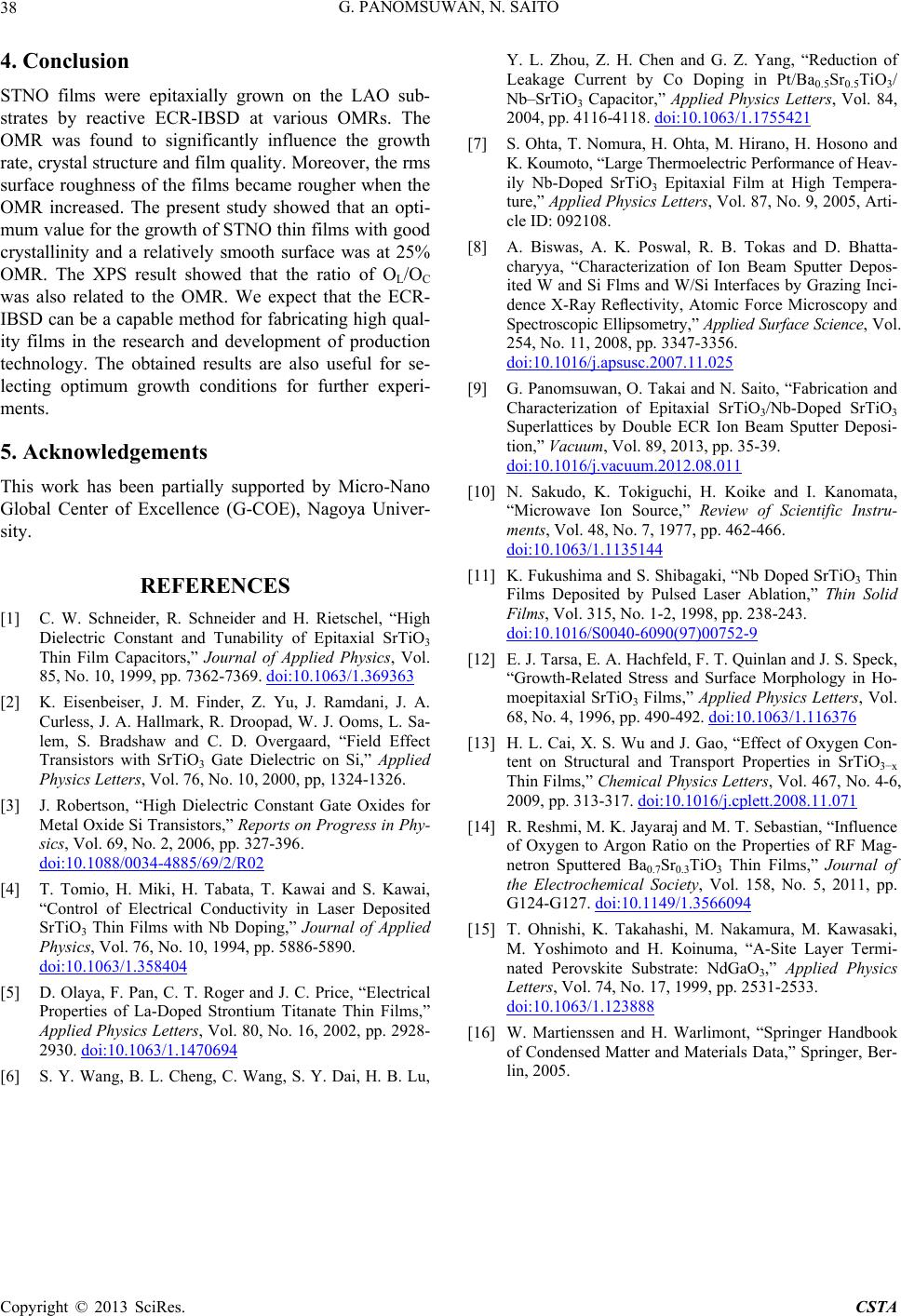
OMR was found to significantly influence the growth
rate, crystal structure and film quality. Moreover, the rms
surface roughness of the films became rougher when the
OMR increased. The present study showed that an opti-
mum value for the growth of STNO thin films with good
crystallinity and a relatively smooth surface was at 25%
OMR. The XPS result showed that the ratio of OL/OC
was also related to the OMR. We expect that the ECR-
IBSD can be a capable method for fabricating high qual-
ity films in the research and development of production
technology. The obtained results are also useful for se-
lecting optimum growth conditions for further experi-
ments.
5. Ackn
This work has been partially
Global Center of Excellence
iver-
sity.
der, R. Schneider and H
nstant and Tunability o
Thin Film Capacitors,” Journal of Applied Physics, Vol.
85, No. 10, 1999, pp. 7362-7369. doi:10.1063/1.369363
[2] K. Eisenbeiser, J. M. Finder, Z. Yu, J. Ramdani, J. A.
Curless, J. A. Hallmark, R. Droopad, W. J. Ooms, L. Sa-
-
lem, S. Bradshaw and C. D. Overgaard, “Field Effect
Transistors with SrTiO3 Gate Dielectric on Si,” Applied
Physics Letters, Vol. 76, No. 10, 2000, pp, 1324-1326.
[3] J. Robertson, “High Dielectric Constant Gate Oxides for
Metal Oxide Si Transistors,” Reports on Progress in Phy
sics, Vol. 69, No. 2, 2006, pp. 327-396.
doi:10.1088/0034-4885/69/2/R02
[4] T. Tomio, H. Miki, H. Tabata, T. Kawa
“Control of Electrical Conductivi
i and S. Kawai,
ty in Laser Deposited
SrTiO3 Thin Films with Nb Doping,” Journal of Applied
Physics, Vol. 76, No. 10, 1994, pp. 5886-5890.
doi:10.1063/1.358404
[5] D. Olaya, F. Pan, C. T. Roger and J. C. Price, “E
Properties of La-Doped
lectrica
Strontium Titanate Thin Films,”
l
Applied Physics Letters, Vol. 80, No. 16, 2002, pp. 2928-
2930. doi:10.1063/1.1470694
[6] S. Y. Wang, B. L. Cheng, C. Wang, S. Y. Dai, H. B. Lu,
Y. L. Zhou, Z. H. Chen and G. Z. Yang, “Reduction of
Leakage Current by Co Doping in Pt/Ba0.5Sr0.5TiO3/
Nb–SrTiO3 Capacitor,” Applied Physics Letters, Vol. 84,
2004, pp. 4116-4118. doi:10.1063/1.1755421
[7] S. Ohta, T. Nomura, H. Ohta, M. Hirano, H. Hosono and
oswal, R. B. Tokas and D. Bhatta-
K. Koumoto, “Large Thermoelectric Performance of Heav-
ily Nb-Doped SrTiO3 Epitaxial Film at High Tempera-
ture,” Applied Physics Letters, Vol. 87, No. 9, 2005, Arti-
cle ID: 092108.
[8] A. Biswas, A. K. P
charyya, “Characterization of Ion Beam Sputter Depos-
ited W and Si Flms and W/Si Interfaces by Grazing Inci-
dence X-Ray Reectivity, Atomic Force Microscopy and
Spectroscopic Ellipsometry,” Applied Surface Science, Vol.
254, No. 11, 2008, pp. 3347-3356.
doi:10.1016/j.apsusc.2007.11.025
[9] G. Panomsuwan, O. Takai and N. Saito, “Fabrication and
Characterization of Epitaxial SrTiO3/Nb-Doped SrTiO3
Superlattices by Double ECR Ion Beam Sputter Deposi-
tion,” Vacuum, Vol. 89, 2013, pp. 35-39.
doi:10.1016/j.vacuum.2012.08.011
[10] N. Sakudo, K. Tokiguchi, H. Koike and I. Kanomata,
“Microwave Ion Source,” Review of Scientific Instru-
ments, Vol. 48, No. 7, 1977, pp. 462-466.
doi:10.1063/1.1135144
[11] K. Fukushima and S. Shibagaki, “Nb Doped SrTiO Thin
3
Films Deposited by Pulsed Laser Ablation,” Thin Solid
Films, Vol. 315, No. 1-2, 1998, pp. 238-243.
doi:10.1016/S0040-6090(97)00752-9
[12] E. J. Tarsa, E. A. Hachfeld, F. T. Quinlan and J. S. Speck,
“Growth-Related Stress and Surface Morphology in Ho-
moepitaxial SrTiO3 Films,” Applied Physics Letters, Vol.
68, No. 4, 1996, pp. 490-492. doi:10.1063/1.116376
[13] H. L. Cai, X. S. Wu and J. Gao, “Effect of Oxygen Con-
tent on Structural and Transport Properties in SrTiO3x
Thin Films,” Chemical Physics Letters, Vol. 467, No. 4-6,
2009, pp. 313-317. doi:10.1016/j.cplett.2008.11.071
[14] R. Reshmi, M. K. Jayaraj and M. T. Sebastian, “Influence
of Oxygen to Argon Ratio on the Properties of RF Mag-
netron Sputtered Ba0.7Sr0.3TiO3 Thin Films,” Journal of
the Electrochemical Society, Vol. 158, No. 5, 2011, pp.
G124-G127. doi:10.1149/1.3566094
[15] T. Ohnishi, K. Takahashi, M. Nakamura, M. Kawasaki,
M. Yoshimoto and H. Koinuma, “A-Site Layer Termi-
nated Perovskite Substrate: NdGaO3,” Applied Physics
Letters, Vol. 74, No. 17, 1999, pp. 2531-2533.
doi:10.1063/1.123888
[16] W. Martienssen and H. Warlimont, “Springer Handbook
of Condensed Matter and Materials Data,” Springer, Ber-
lin, 2005.