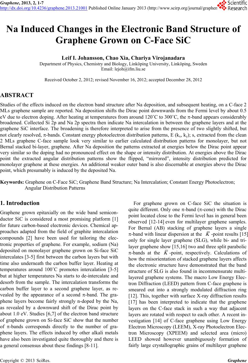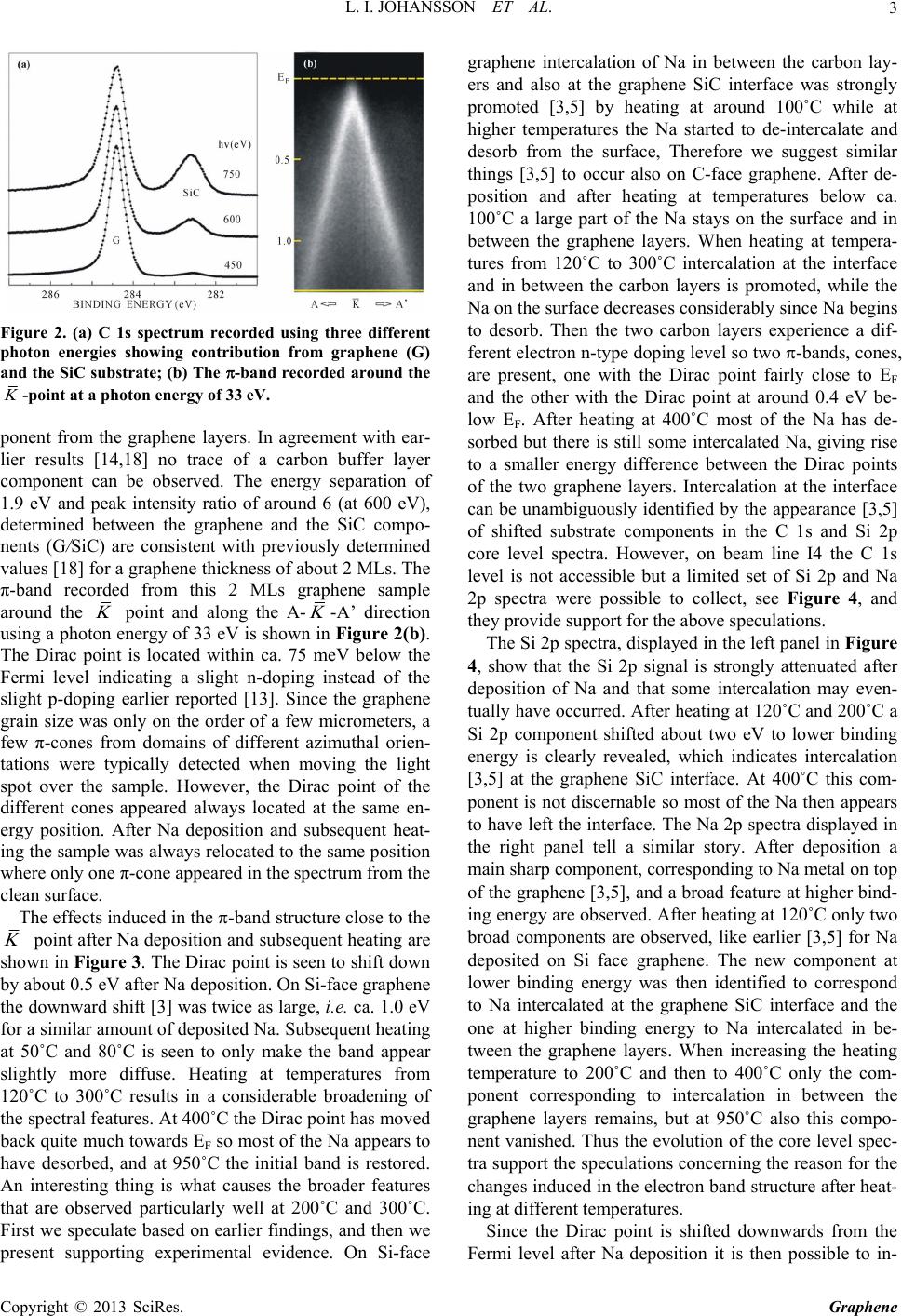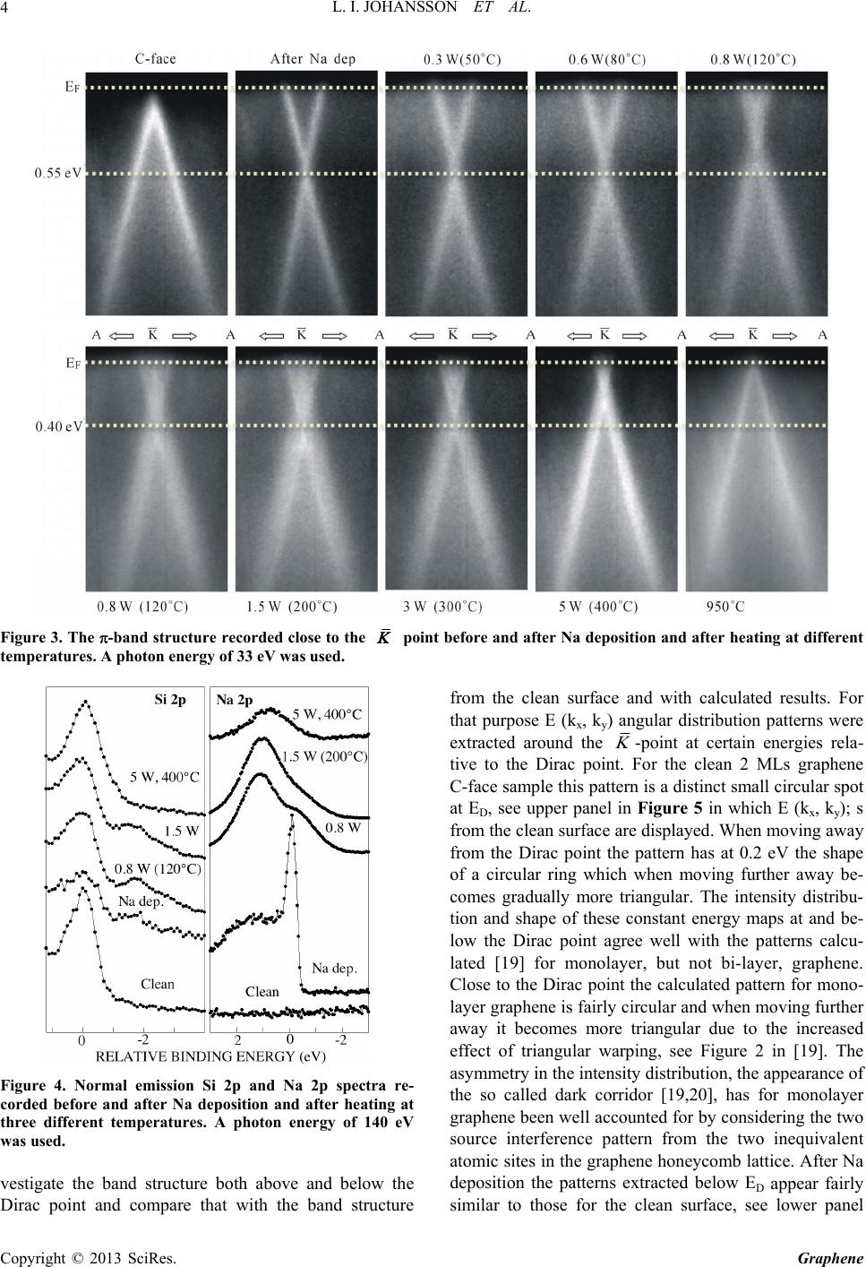
L. I. JOHANSSON ET AL.
6
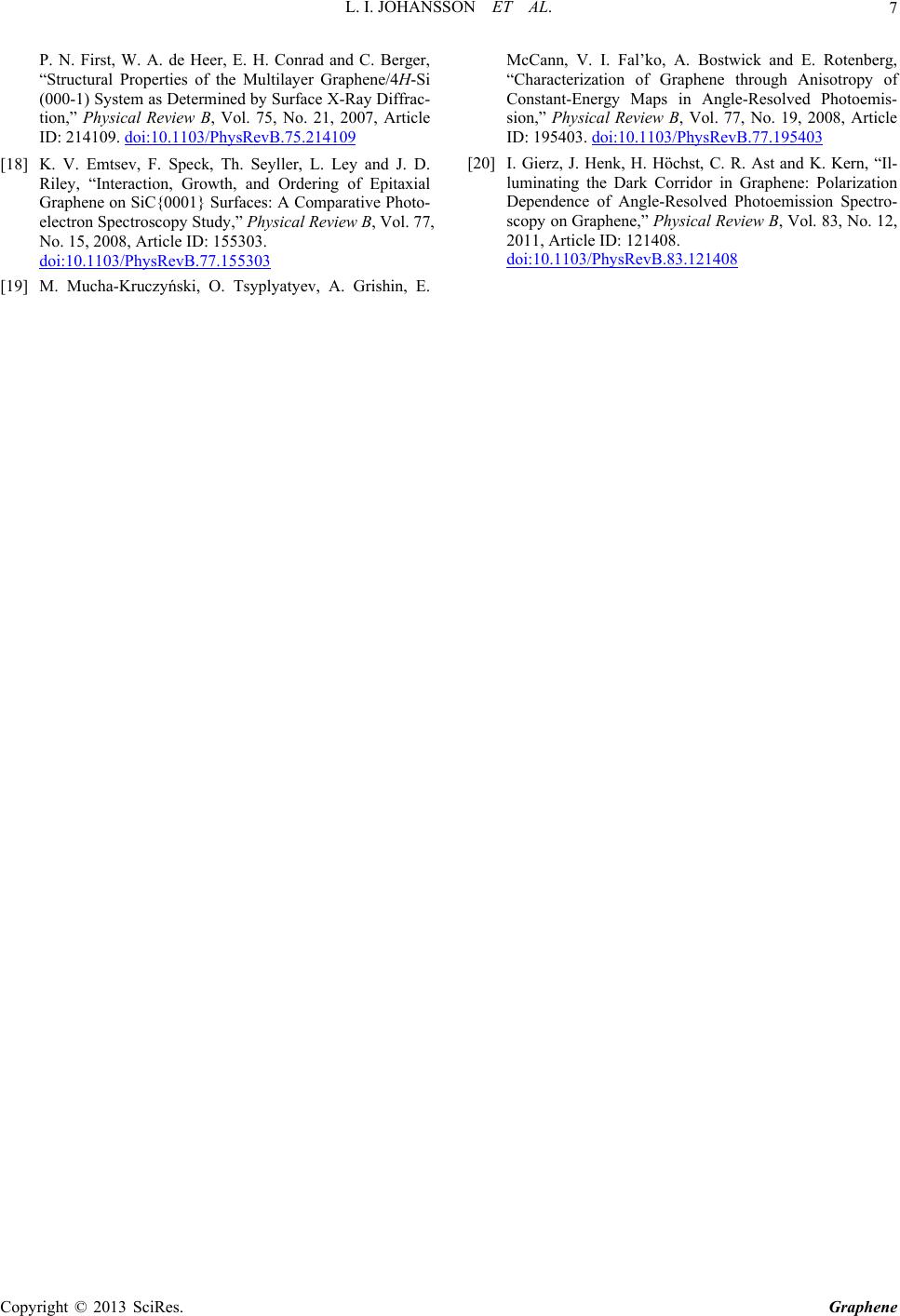
Figure 6. Cuts from the data set recorded after Na deposi-
tion in Figure 5. In a) the cut is along the A-
-A’ direction
and at the
point, i.e. at kx ≈ 1.7 [1/Å]. In b) the cut is
also at the
point but along the Γ-
-
direction. In
c) the cut is along the A-
-A’, direction but at kx ≈ 1.8
[1/Å], see lower panel in Figure 5.
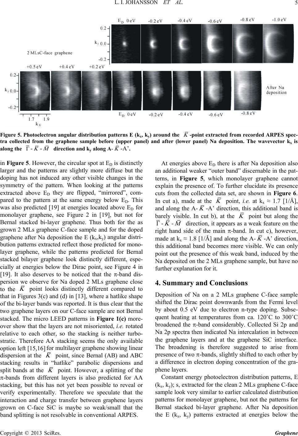
Dirac point appear very similar to those for the clean
sample so the doping did not visibly affect the shape or
intensity distribution. Then at energies above the Dirac
point the angular distribution patterns show the flipped,
“mirrored”, intensity distribution predicted for mono-
layer, but not bi-layer, graphene. The deposited Na in-
duced an additional weaker outer band at energies above
the Dirac point, which calculated results for monolayer
graphene could not account for.
5. Acknowledgements
The authors gratefully acknowledge support from the
European Science Foundation, within the EuroGRA-
PHENE (EPIGRAT) program, and the Swedish Research
Council (#621-2011-4252 and Linnaeus Grant).
REFERENCES
[1] P. N. First, W. A. de Heer, T. Seyller, C. Berger, J. A.
Stroscio and J.-S. Moon, “Epitaxial Graphenes on Silicon
Carbide,” MRS Bulletin, Vol. 35, No. 4, 2010, pp. 296-
305. doi:10.1557/mrs2010.552
[2] M. S. Dresselhaus and G. Dresselhaus, “Intercalation
Compounds of Graphite,” Advances in Physics, Vol. 51,
No. 1, 2002, pp. 1-186. doi:10.1080/00018730110113644
[3] S. Watcharinyanon, L. I. Johansson, C. Xia and C. Viro-
janadara, “Changes in Structural and Electronic Proper-
ties of Graphene Grown on 6H-SiC(0001) Induced by Na
Deposition,” Journal of Applied Physics, Vol. 111, No. 8,
2012, Article ID: 083711. doi:10.1063/1.4704396
[4] A. Sandin, T. Jayasekera, J. E. Rowe, K. W. Kim, M. B.
Nardelli and D. B. Dougherty, “Multiple Coexisting In-
tercalation Structures of Sodium in Epitaxial Graphene-
SiC Interfaces,” Physical Review B, Vol. 85, 2012, Arti-
cle ID: 125410. doi:10.1103/PhysRevB.85.125410
[5] C. Xia, S. Watcharinyanon, A. A. Zakharov, L. I. Johans-
son, R. Yakimova and C. Virojanadara, “Detailed Studies
of Na Intercalation on Furnace-Grown Graphene on 6H-
SiC(0001),” in Press.
[6] T. Ohta, A. Bostwick, J. L. Mc-Chesney, T. Seyller, K.
Horn and E. Rotenberg, “Interlayer Interaction and Elec-
tronic Screening in Multilayer Graphene Investigated with
Angle-Resolved Photoemission Spectroscopy,” Physical
Review Letters, Vol. 98, No. 20, 2007, Article ID: 206802.
doi:10.1103/PhysRevLett.98.206802
[7] A. Bostwick, T. Ohta, T. Seyller, K. Horn and E. Roten-
berg, “Quasiparticle Dynamics in Graphen,” Nature Phys-
ics, Vol. 3, 2007, pp. 36-40. doi:10.1038/nphys477
[8] A. A. Bostwick, F. Speck, T. Seyller, K. Horn, M. Polini,
R. Asgari, A. H. MacDonald and E. Rotenberg, “Obser-
vation of Plasmarons in Quasi-Freestanding Doped Gra-
phene,” Science, Vol. 328, No. 5981, 2010, pp. 999-1002.
doi:10.1126/science.1186489
[9] C. Virojanadara, S. Watcharinyanon, A. A. Zakharov and
L. I. Johansson, “Epitaxial Graphene on 6H-SiC and Li
Intercalation,” Physical Review B, Vol. 82, No. 20, 2010,
Article ID: 205402. doi:10.1103/PhysRevB.82.205402
[10] S. Watcharinyanon, C. Virojanadara and L. I. Johansson,
“Rb and Cs Deposition on Epitaxial Graphene Grown on
6H-SiC(0001),” Surface Science, Vol. 605, No. 21-22,
2011, pp. 1918-1922. doi:10.1016/j.susc.2011.07.007
[11] A. L. Walter, A. Bostwick, K.-J. Jeon, F. Speck, M. Os-
tler, T. Seyller, L. Moreschini, Y. J. Chang, M. Polini, R.
Asgari, A. H. MacDonald, K. Horn and E. Rotenberg,
“Effective Screening and the Plasmaron Bands in Gra-
phene,” Physical Review B, Vol. 84, No. 8, 2011, Article
ID: 085410. doi:10.1103/PhysRevB.84.085410
[12] M. Sprinkle, D. Siegel, Y. Hu, J. Hicks, A. Tejeda, A.
Taleb-Ibrahimi, P. Le Fe’vre, F. Bertran, S. Vizzini, H.
Enriquez, S. Chiang, P. Soukiassian, C. Berger, W. A. de
Heer, A. Lanzara and E. H. Conrad, “First Direct Obser-
vation of a Nearly Ideal Graphene Band Structure,” Phy-
sical Review Letters, Vol. 103, No. 22, 2009, Article ID:
226803. doi:10.1103/PhysRevLett.103.226803
[13] D. A. Siegel, C. G. Hwang, A. W. Fedorov and A. Lan-
zara, “Quasifreestanding Multilayer Graphene Films on
the Carbon Face of SiC,” Physical Review B, Vol. 81, No.
24, 2010, Article ID: 241417.
doi:10.1103/PhysRevB.81.241417
[14] L. I. Johansson, S. Watcharinyanon, A. A. Zakharov, T.
Iakimo, R. Yakimova and C. Virojanadara, “Stacking of
Adjacent Graphene Layers Grown on C-Face SiC,” Phy-
sical Review B, Vol. 84, No. 12, 2011, Article ID: 125405.
doi:10.1103/PhysRevB.84.125405
[15] S. Latil, V. Meunier and L. Henrard, “Massless Fermions
in Multilayer Graphitic Systems with Misoriented Layers:
Ab Initio Calculations and Experimental Fingerprints,”
Physical Review B, Vol. 76, No. 20, 2007, Article ID:
201402. doi:10.1103/PhysRevB.76.201402
[16] S. Latil and L. Henrard, “Charge Carriers in Few-Layer
Graphene Films,” Physical Review Letters, Vol. 97, No. 3,
2006, Article ID: 036803.
doi:10.1103/PhysRevLett.97.036803
[17] J. Hass, R. Feng, J. E. Millan-Otoya, X. Li, M. Sprinkle,
Copyright © 2013 SciRes. Graphene