Open Journal of Applied Sciences, 2013, 3, 65-67
Published Online March 2013 (http://www.scirp.org/journal/ojapps)
Copyright © 2013 SciRes. OJAppS
A Programmable High Speed Vision System with
Superscalar PE and Its Parallel Computing Language
Jie Yang, Cong Shi, Xitian Long, Nanjian Wu
Institute of Semiconductors, Chinese Academy of Sciences, Beijing, China
Email: yangjie@semi.ac.cn
Received 2012
ABSTRACT
Pixe l-parallel PE and SIMD architectures are widely used in high-speed image processing to enhance computing power.
With fully exploiting the data level parallelism of low- and middle-level image processing, SIMD architecture is able to
finish great amount of computation with much less instruction cycle thus satisfy the high-speed system requirement.
The main computation parts in those SIMD image processing hardware is known as PE (processing element) and it is
responsible for transferring, storing and processing the image data. This paper describes a high-speed vision system
with superscalar PE to enhance system performance and its dedicated parallel computing language specifically devel-
oped for this vision system. The vision system can achieve motion detection at more than 2000fps and face detection at
more than 100 fps which overwhelms some general serial CPUs in the same applications.
Keywords: High-Speed Vision System; SIMD; Superscalar; PE
1. Introduction
Researchers have been interested in high -speed vision
system for decades [1]. It can be applied in many fields,
such as real-time object-tracking, machine vision, indus-
try controls. Traditional machine vision systems which
are composed of image sensor and general-purpose pro-
cessor have heavy I/O load induced by large amount of
image data transfer and lack of computational power for
low- and middle-level processing. Our previous design [2]
using multi-level parallel processors to fully cover low-,
middle-, and high-level image processing and with dedi-
cated programming language this design can finish vari-
ous high-speed image processing tasks. However the
image sensor exposure and data transfer of every frame
consume large amount of time and instruction cycles thus
greatly reduce the processing rate of our vision system.
In this paper, we apply a superscalar PE to our pre-
vious architecture. The new PE structure is capable of
simultaneously executing an image transfer instruction
and an image processing instruction, thus frame pipeline
is achieved. A calculated PE performance improvement
is nearly 100% for some algorithms. A parallel compu-
ting language and its compiler and assembler are devel-
oped to support the new PE programming and related
further designs.
This paper proceeds as follows. In section II, we will
describe the architecture of our vision system, the new
PE structure and the parallel computing language. In sec-
tion III, the FPGA implementation is presented. And
finally we draw conclusion in section IV.
2. Architecture of the System
2.1. System Architecture
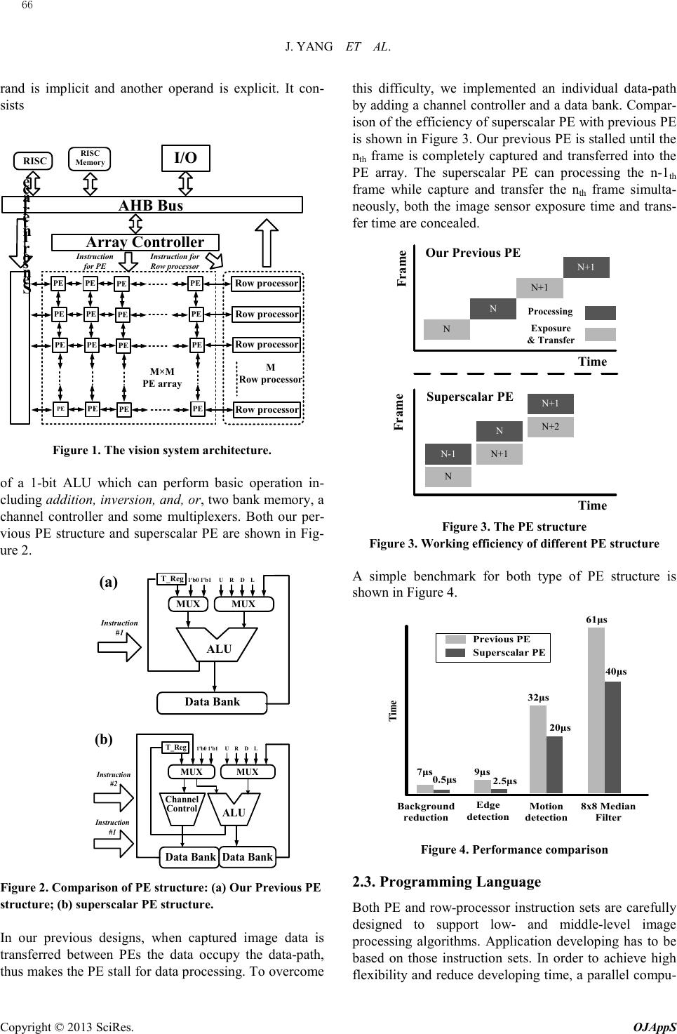
The architecture of the proposed vision system is pre-
sented in fig.1. It consists of a pixel-parallel PE array, a
row-parallel processor, a RISC core, an on-chip AHB
bus, a sensor controller and an I/O module. The sensor
interface is responsible for sub sampling the image plane.
The PE array is composed of M×M identical PEs, each
PE is a single bit processor connected with its up, down,
left, right PE neighborhoods. The row-parallel processors
serve as the interface of PE array with the RISC core and
carry out middle-level image processing. The RISC core
controls the whole system and performs high-level image
pro c e ssing.
In summary, the system architecture integrates three
different kinds of processors targets at different levels of
image processing. It is specifically designed for
high -speed image processing.
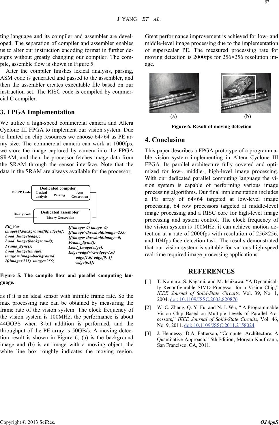
2.2. PE Structure
Every PE cell is connected to its nearest four neighbors
in four directions: up, right, down, left. All PEs receive
the same instructions and operate in an SIMD fashion.
PE is built in accumulator architecture [3] that one ope-
J. YANG ET AL.
Copyright © 2013 SciRes. OJAppS
rand is implicit and another operand is explicit. It con-
sists
RISC RISC
Memory
AHB Bus
S
e
n
s
o
r
I
n
t
e
r
f
a
c
e
PE PE PE
PE PE PE
PE PE PE
PE
PE
PE
PE PE PE PE
Row processor
Row processor
Row processor
Row processor
M×M
PE array
M
Row processor
Array Controller
Instruction
for PE
Instruction for
Row processor
I/O
Figure 1. The vision system architecture.
of a 1-bit ALU which can perform basic operation in-
cluding addition, inversion, and, or, two bank memory, a
channel controller and some multiplexer s. Both our per-
vious PE structure and superscalar PE are shown in Fig-
ure 2.
Figure 2. Comparison of PE structure: (a) Our Previous PE
structure; (b) superscalar PE structure.
In our previous designs, when captured image data is
transferred between PEs the data occupy the data-path,
thus makes the PE stall for data processing. To overcome
this difficulty, we implemented an individual data-path
by adding a channel controller and a data bank. Compar-
ison of the ef ficienc y of superscalar PE with previous PE
is shown in Figure 3. Our previous PE is stalled until the
nth frame is completely captured and transferred into the
PE array. The superscalar PE can processing the n-1th
frame while capture and transfer the nth frame simulta-
neously, both the image sensor exposure time and trans-
fer time are concealed.
Figure 3. The PE structure
Figure 3. Working efficiency of different PE structure
A simple benchmark for both type of PE structure is
shown in Figure 4.
Figure 4. Performance comparison
2.3. Programming Language
Both PE and row-processor instruction sets are carefully
designed to support low- and middle-level image
processing algorithms. Application developing has to be
based on those instruction sets. In order to achieve high
flexibility and reduce developing time, a parallel compu-
N
N
N+1
N+1
N-1
N
N
N+1
Time
Time
Frame
Processing
Exposure
& Transfer
N+1
N+2
Our Previous PE
Superscalar PE
Frame
ALU
MUX
MUX
U RD L
T_Reg
1'b0 1'b1
Data Bank
Instruction
#1
(a)
ALU
MUX
MUX
U RDL
T_Reg
1'b0 1'b1
Data Bank
Control
Channel
Data Bank
Instruction
#2
(b)
Instruction
#1
Time
Background
reduction
Edge
detection
Motion
detection
8x8 Median
Filter
7μs 9μs
32μs
Previous PE
Superscalar PE
61μs
0.5μs2.5μs
20μs
40μs
J. YANG ET AL.
Copyright © 2013 SciRes. OJAppS
ting language and its compiler and assembler are devel-
oped. The separation of compiler and assembler enables
us to alter our instruction encoding format in further de-
signs without greatly changing our compiler. The com-
pile, assemble flow is shown in Figure 5.
After the compiler finishes lexical analysis, parsing,
ASM code is generated and passed to the assembler, and
then the assembler creates executable file based on our
instruction set. The RISC code is compiled by commer-
cial C compiler.
3. FPGA Implementation
We utilize a high-speed commercial camera and Altera
Cyclone III FPGA to implement our vision system. Due
to limited on chip resources we choose 64×64 as PE ar-
ray size. The commercial camera can work at 1000fps,
we store the image captured by camera into the FPGA
SRAM, and then the processor fetches image data from
the SRAM through the sensor interface. Note that the
data in the SRAM are always available for the processor,
Figure 5. The compile flow and parallel computing lan-
guage.
as if it is an ideal sensor with infinite frame rate. So the
max processing rate can be obtained by measuring the
frame rate of the vision system. The clock frequency of
the vision system is 100MHz, the performance is about
44GOPS when 8-bit addition is performed, and the
throughput of the PE array is 50GB/s. A moving detec-
tion result is shown in Figure 6, (a) is the background
image and (b) is an image with a moving object, the
white line box roughly indicates the moving region.
Great performance improvement is achieved for low- and
middle-level image processing due to the implementation
of superscalar PE. The measured processing rate for
moving detection is 2000fps for 256×256 resolution im-
age.
Figure 6. Result of moving detection
4. Conclusion
This paper describes a FPGA prototype of a programma-
ble vision system implementing in Altera Cyclone III
FPGA. Its parallel architecture fully covered and opti-
mized for low-, middle-, high-level image processing.
With our dedicated parallel computing language the vi-
sion system is capable of performing various image
processing algorithms. Our final implementation includes
a PE array of 64×64 targeted at low-level image
processing, 64 row processors targeted at middle-level
image processing and a RISC core for high-level image
processing and system control. The clock frequency of
the vision system is 100MHz. it can achieve motion de-
tection at a rate of 2000fps with resolution of 256×256,
and 104fps face detection task. The results demonstrated
that our vision system is suitable for various high-speed
real-time required image processing applications.
REFERENCES
[1] T. Komuro, S. Kagami, and M. Ishikawa, “A Dynamical-
ly Reconfigurable SIMD Processor for a Vision Chip,”
IEEE Journal of Solid-State Circuits, Vol. 39, No. 1,
2004. doi: 10.1109/JSSC.2003.820876
[2] W .C. Zhang, Q. Y. Fu, and N. J. Wu, “ A Programmable
Vision Chip Based on Multiple Levels of Parallel Pro-
cessors,” IEEE Journal of Solid-State Circuits, Vol. 46,
No. 9, 2011. doi: 10.1109/JSSC.2011.2158024
[3] J. Hennessy, D.A. Patterson, “Computer Architecture: A
Quantitative Approach,” 5th Edition, Morgan Kaufmann,
San Francisco, CA, 2011.
PE RP CodeLexical
analysis Parsing
Binary Generation
Dedicated compiler
Asm
Generation
Dedicated assembler
Binary code
PE_Var
image[8],background[8],edge[8];
Load_Image(edge);
Load_Image(background);
Frame_Sync();
Load_Image(image);
image = image-background
If(image>255) image=255;
If(image<0) image=0;
If(image>threshold)image=255;
If(image<threshold)image=0;
Frame_Sync();
Load_Image(edge);
Edge=edge>>2-edge{-1,0}
-edge{1,0}-edge{0,-1}
-edge{0,1};
(a)
(b)