 Optics and Photonics Journal, 2012, 2, 344-351 http://dx.doi.org/10.4236/opj.2012.24043 Published Online December 2012 (http://www.SciRP.org/journal/opj) Analysis of As2S3-Ti: LiNbO3 Taper Couplers Using Supermode Theory Xin Xia, Yifeng Zhou, Christi K. Madsen Department of Electrical and Computer Engineering, Texas A&M University, College Station, USA Email: cmadsen@tamu.edu Received October 16, 2012; revised November 14, 2012; accepted November 24, 2012 ABSTRACT In this work, we develop a simulation method based on supermode theory and transfer matrix formalism, and then apply it to the analysis and design of taper couplers for vertically integrated As2S3 and Ti: LiNbO3 hybrid waveguides. Test structures based on taper couplers are fabricated and characterized. The experimental results confirm the validity of the modeling method, which in turn, is used to analyze the fabricated couplers. Keywords: Optical Waveguides; Couplers; Coupled Mode Analysis 1. Introduction As study on integrated Optics proceeds, several schemes with regard to materials and structures were developed, such as silicon-on-insulator, chalcogenide glass wave- guides, III-V semiconductor waveguides and titanium diffused waveguides. While different schemes have their own merits and shortcomings, reciprocal benefits can be obtained from integration of them, namely, the hybrid waveguides. For example, preliminary result was re- ported on As2S3-on-Ti: LiNbO3 hybrid waveguide de- vices [1,2], which benefit from the high index contrast of As2S3 and easy connection with commercial single mode fibers. For integration of different waveguides, light cou- pling is the key. A directional coupler is the simplest functional device to couple light by transferring energy between two waveguides. However, in practice its cou- pling efficiency can be fairly low due to the phase mis- match and small tolerance to fabrication errors. Alterna- tively grating and taper couplers are used, and taper cou- plers are generally preferred owing to its simplicity in design and fabrication. Despite diverse forms, the general taper coupler is composed of two parallel waveguides placed in close proximity: one is uniform whereas at one end of the other one, the width is gradually varied. Two ends of the taper match the wave guiding properties of two waveguides, so the mode is transformed gradually from one into another during propagation in the taper. Although the principle is intuitively quite simple, the design in most cases is conservative because of the lack of precise modeling guidelines and accurate modeling tools [3]. A lot of theoretical study was carried out to investigate them, and different approaches were devel- oped. Lee et al. proposed an equivalent waveguide con- cept employing a conformal mapping method, which was combined with the Beam Propagation Method (BPM) to conduct analysis [4]. In [3], tapered waveguides were analyzed by considering the whole taper as a succession of short linear taper fragments and modeling each of them using a two-dimensional BPM that solves directly the Helmholtz equation. However, most of the early work focused on correct- ing simulation methods to improve the accuracy, and the underlying physical mechanism governing the power transfer was not described [5]. Therefore, few guidelines can be found for designers. Thus more and more re- searchers began to look into taper couplers from the an- gle of supermodes, i.e. local modes. In [5], Xia et al. de- fined and distinguished between the resonant coupling and adiabatic coupling from the view of supermodes [5]. Resonant couplers are compact and simple but highly sensitive to unavoidable variations during fabrication [5]. Adiabatic couplers , on the contrary, don’t require exact control of taper length and gap, but need longer lengths [6]. Sun et al. conducted a series of studies on the be- havior of supermodes in adiabatic couplers [6,7] and derived a mathematical expression of the shortest adia- batic tapers [6]. As such theoretical work contributed a lot to our understanding of taper couplers, the study on issues of practical application and modeling is still lack- ing. In practice, we often need to balance the taper length and the coupling efficiency, since we may not have suf- ficient space to fulfill the adiabatic condition, and we may want certain coupling efficiency that is not neces- sarily 100%. Mach-Zehnder interference filters, for ex- ample, typically use 3 dB couplers. Moreover, the mate- C opyright © 2012 SciRes. OPJ  X. XIA ET AL. 345 rials and structures used may limit the coupling. Thus, there are a lot of efficient but non-adiabatic taper cou- plers desired in practice. In published papers most simulations were conducted based on beam propagation method (BPM) [8]. BPM calculates the electromagnetic fields during light propa- gation process and gives distributions of electric and magnetic fields. It is highly accurate as long as certain assumptions are met. However, limited knowledge of underlying mechanism can be obtained from the simula- tion process, so it is widely used to as a means of exam- ining the designed taper coupler instead of guiding the design at the first place. Alternatively, the modeling of taper couplers can be based on the concept of modes us- ing the coupled mode theory, which can provide insights to the mode evolvement in the coupler and thus provide immediate guidelines for design. 2. Modeling Methods A taper coupler, which consists of two adjacent wave- guides, can be regarded as a modified directional coupler. In each waveguide, only one mode is allowed to propa- gate. The coupled mode theory analyzes the coupled waveguides by taking one waveguide as the subject and studying the influence of the perturbation imposed by the presence of the other one. The supermode theory, how- ever, views the coupled waveguides as a whole system, i.e. a composite two-waveguide structure, and studies the normalized local modes of the system, which are called supermodes. Nevertheless, both theories describe mode coupling for scenarios that coupled waveguides are in- variable along the propagation direction. But the taper coupler is a varying structure where the width of one of the waveguides is constantly changing along the propa- gation direction. However, the coupler can be divided into a succession of infinitely short sections. The length of each section is so small that the width can be regarded as invariant. So the simulation of a taper coupler can be divided into two steps: modeling of individual divisions and a cascade of individual models. For each division, as the width is deemed constant, it is actually a simple di- rectional coupler, in which there are fundamental super- mode and first order supermode, named as even mode (Ee) and odd mode (Eo) respectively according to the symmetry of their field distributions. The total field is a linear combination of the even and odd mode. If the propagation constants of modes in indivi- dual waveguides are the same, namely, they are phase matched, two lobes of even and odd mode have the same size. If two propagation constants are different, that is, the phases are mismatched, the symmetry of lobes of Ee and Eo is broken, and their shapes are different. When phase mismatch is large, two waveguides are effectively decoupled: a wave propagating in either one is virtually unaffected by the existence of the other, and the super- modes of the composite structure just become those of the individual waveguides [9]. δ is defined as the differ- ence of the propagation constants of two individual modes while βc is for two supermodes in a similar way in (1): 21 and 22 eo c (1) As shown in Figure 1, if δ is much smaller than 0, most energy of the even mode is located in waveguide 1 while if it is much larger than 0, most energy is located in waveguide 2. The opposite is true for the odd mode. So, the essence of taper coupling is to spatially transfer the energy of a supermode (even mode) from one waveguide to the other by designing the tapered waveguide so that δ sweeps from a negative value to a positive value while suppressing the coupling to the other supermode (odd mode) [6]. The larger scope δ covers, the more thorough the energy transfer is. Ideally, δ changes from negative infinity to positive infinity, whereas in practice, the scope is determined by the materials and structures. Solving the coupled mode equations by substituting the general supermode solutions into them, we can obtain the expressions of supermodes and the relationship be- tween the phase mismatch of supermodes (βc) and that of individual modes (δ) [7] 22 c 2 (2) As δ and βc are known, the coupling strength κ [9] can be calculated. Then we have a complete mathematical description of the model with parameter δ, κ and βc. Fol- lowing the same method, models of all the divisions in the taper coupler can be built. Subsequently, transfer matrix formalism is derived to cascade all the models based on coupled mode equations. In the matrix form, the solution to coupled mode equa- tions is (3). 1i 2 i 1 i 2 cossin e sin esin e 0 cossin e0 cc c iz z cc cc z cc c Ez j zz Ez jj zz E j zz E (3) where 10E and 20E are the input electric fields in waveguide 1 and 2 respectively. Let 0 and re-form the equation to obtain the expression of vector, let 0 zz zz z to re-write (3), substitute the vector expres- sion into it, and we arrive at the transfer matrix formal- ism relating the model at to the model at 0 zz Copyright © 2012 SciRes. OPJ 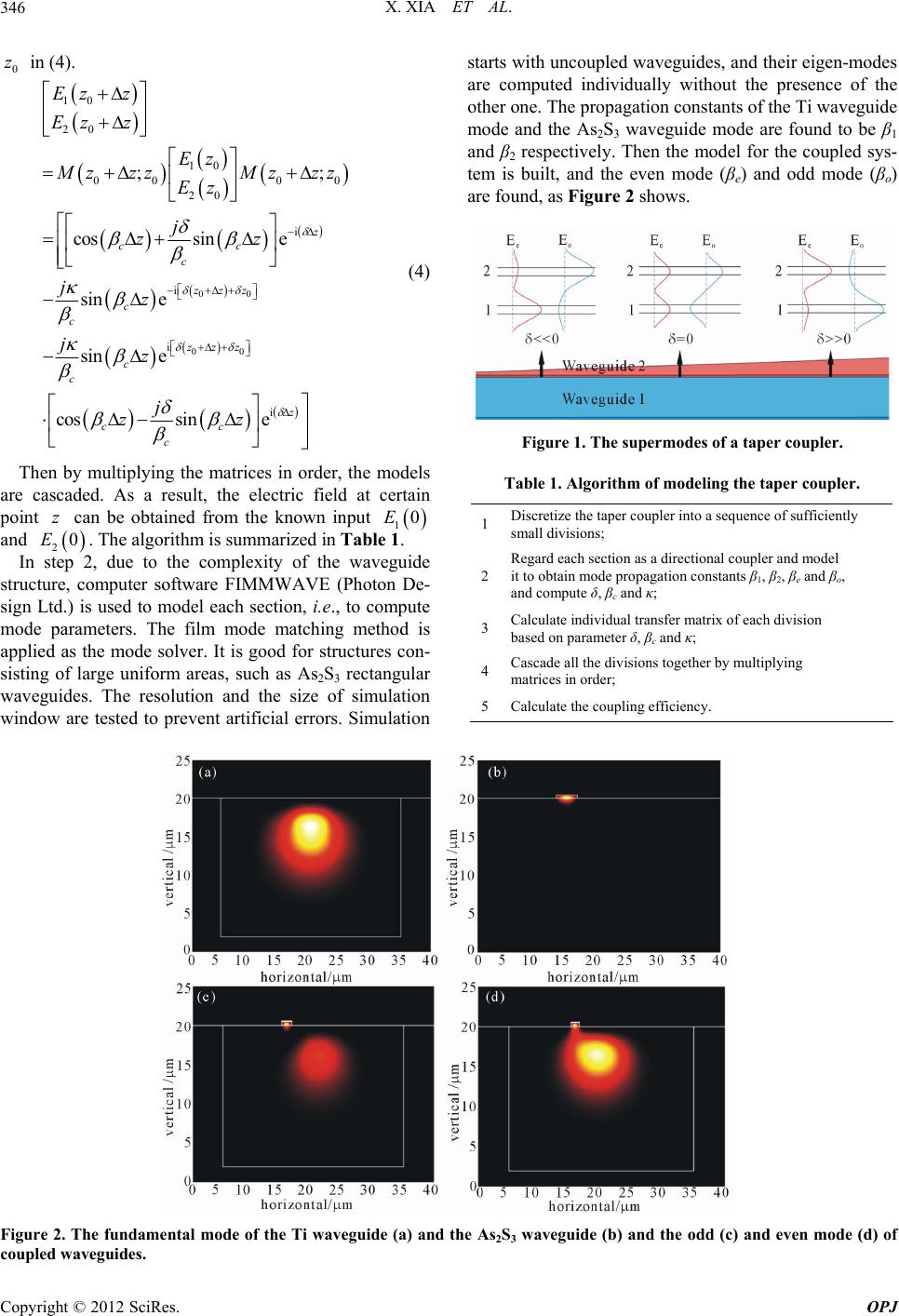 X. XIA ET AL. Copyright © 2012 SciRes. OPJ 346 0 z in (4). 00 00 10 20 10 00 00 20 i i i i ; cossin e sin e sin e cossin e z cc c zzz c c zzz c c z cc c Ez z Ez z Ez ; zzz Mzzz Ez j zz jz jz j zz (4) starts with uncoupled waveguides, and their eigen-modes are computed individually without the presence of the other one. The propagation constants of the Ti waveguide mode and the As2S3 waveguide mode are found to be β1 and β2 respectively. Then the model for the coupled sys- tem is built, and the even mode (βe) and odd mode (βo) are found, as Figure 2 shows. Figure 1. The supermodes of a taper coupler. Then by multiplying the matrices in order, the models are cascaded. As a result, the electric field at certain point can be obtained from the known input z 10E and . The algorithm is summarized in Table 1. 2 E 0 Table 1. Algorithm of modeling the taper coupler. 1Discretize the taper coupler into a sequence of sufficiently small divisions; 2 Regard each section as a directional coupler and model it to obtain mode propagation constants β1, β2, βe and βo, and compute δ, βc and κ; 3Calculate individual transfer matrix of each division based on parameter δ, βc and κ; 4Cascade all the divisions together by multiplying matrices in order; 5Calculate the coupling efficiency. In step 2, due to the complexity of the waveguide structure, computer software FIMMWAVE (Photon De- sign Ltd.) is used to model each section, i.e., to compute mode parameters. The film mode matching method is applied as the mode solver. It is good for structures con- sisting of large uniform areas, such as As2S3 rectangular waveguides. The resolution and the size of simulation window are tested to prevent artificial errors. Simulation Figure 2. The fundamental mode of the Ti waveguide (a) and the As2S3 waveguide (b) and the odd (c) and even mode (d) of coupled waveguides. 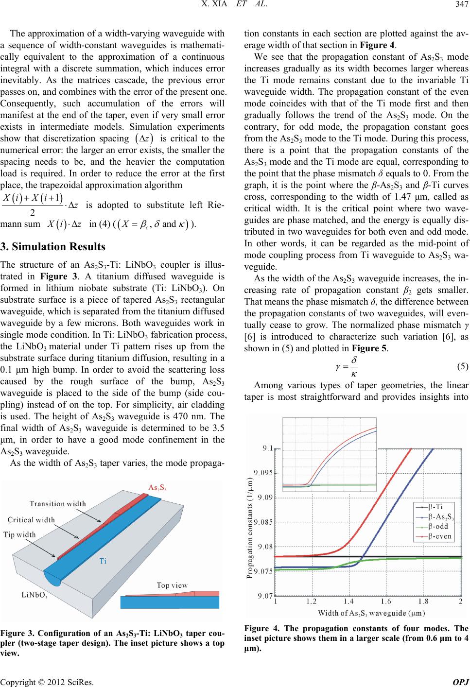 X. XIA ET AL. 347 The approximation of a width-varying waveguide with a sequence of width-constant waveguides is mathemati- cally equivalent to the approximation of a continuous integral with a discrete summation, which induces error inevitably. As the matrices cascade, the previous error passes on, and combines with the error of the present one. Consequently, such accumulation of the errors will manifest at the end of the taper, even if very small error exists in intermediate models. Simulation experiments show that discretization spacing is critical to the numerical error: the larger an error exists, the smaller the spacing needs to be, and the heavier the computation load is required. In order to reduce the error at the first place, the trapezoidal approximation algorithm z 1 2 Xi Xiz is adopted to substitute left Rie- mann sum iz in (4) ( ,and c X ). 3. Simulation Results The structure of an As2S3-Ti: LiNbO3 coupler is illus- trated in Figure 3. A titanium diffused waveguide is formed in lithium niobate substrate (Ti: LiNbO3). On substrate surface is a piece of tapered As2S3 rectangular waveguide, which is separated from the titanium diffused waveguide by a few microns. Both waveguides work in single mode condition. In Ti: LiNbO3 fabrication process, the LiNbO3 material under Ti pattern rises up from the substrate surface during titanium diffusion, resulting in a 0.1 μm high bump. In order to avoid the scattering loss caused by the rough surface of the bump, As2S3 waveguide is placed to the side of the bump (side cou- pling) instead of on the top. For simplicity, air cladding is used. The height of As2S3 waveguide is 470 nm. The final width of As2S3 waveguide is determined to be 3.5 μm, in order to have a good mode confinement in the As2S3 waveguide. As the width of As2S3 taper varies, the mode propaga- Figure 3. Configuration of an As2S3-Ti: LiNbO3 taper cou- pler (two-stage taper design). The inset picture shows a top view. tion constants in each section are plotted against the av- erage width of that section in Figure 4. We see that the propagation constant of As2S3 mode increases gradually as its width becomes larger whereas the Ti mode remains constant due to the invariable Ti waveguide width. The propagation constant of the even mode coincides with that of the Ti mode first and then gradually follows the trend of the As2S3 mode. On the contrary, for odd mode, the propagation constant goes from the As2S3 mode to the Ti mode. During this process, there is a point that the propagation constants of the As2S3 mode and the Ti mode are equal, corresponding to the point that the phase mismatch δ equals to 0. From the graph, it is the point where the β-As2S3 and β-Ti curves cross, corresponding to the width of 1.47 μm, called as critical width. It is the critical point where two wave- guides are phase matched, and the energy is equally dis- tributed in two waveguides for both even and odd mode. In other words, it can be regarded as the mid-point of mode coupling process from Ti waveguide to As2S3 wa- veguide. As the width of the As2S3 waveguide increases, the in- creasing rate of propagation constant β2 gets smaller. That means the phase mismatch δ, the difference between the propagation constants of two waveguides, will even- tually cease to grow. The normalized phase mismatch γ [6] is introduced to characterize such variation [6], as shown in (5) and plotted in Figure 5. (5) Among various types of taper geometries, the linear taper is most straightforward and provides insights into Figure 4. The propagation constants of four modes. The inset picture shows them in a larger scale (from 0.6 μm to 4 μm). Copyright © 2012 SciRes. OPJ 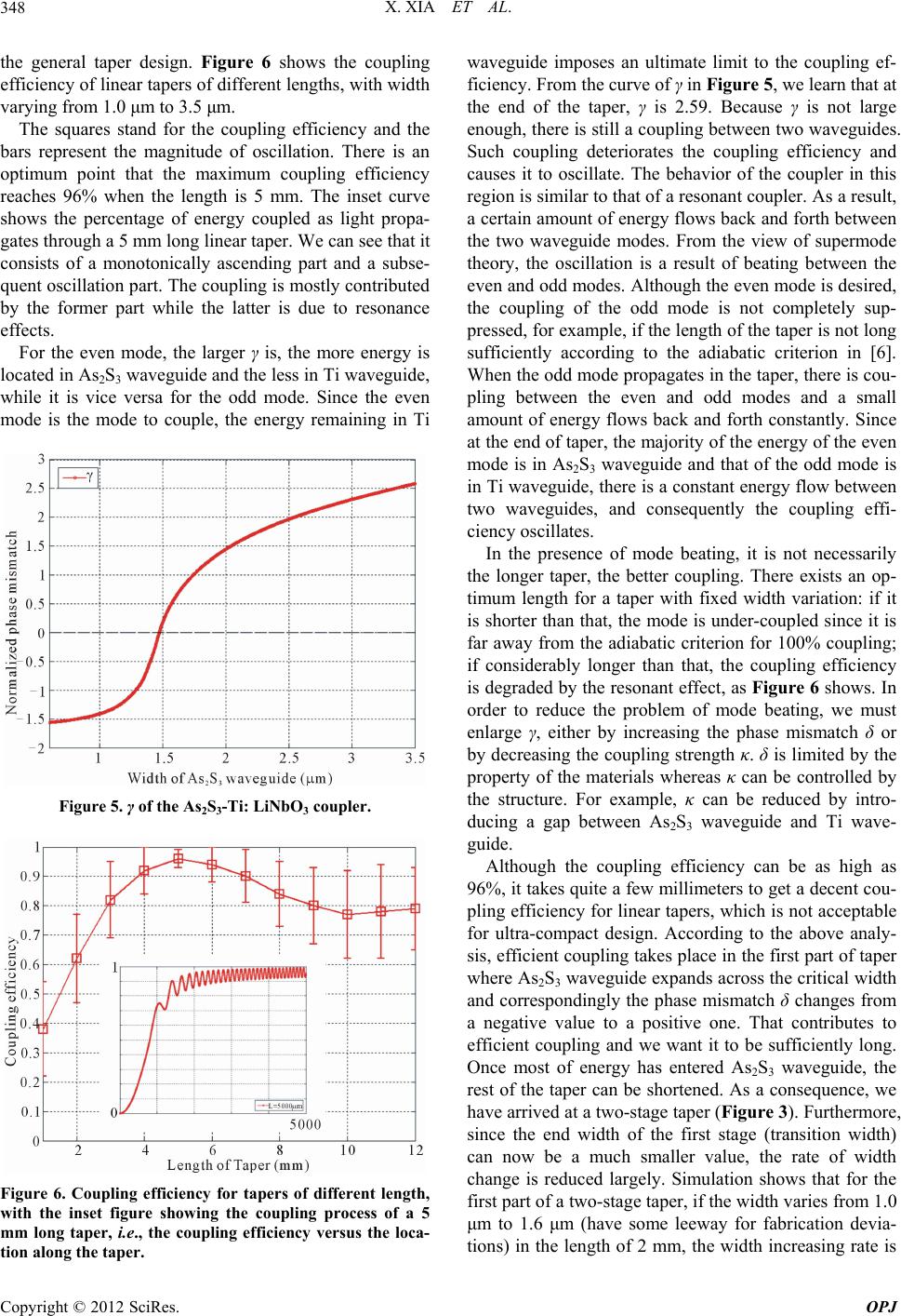 X. XIA ET AL. 348 the general taper design. Figure 6 shows the coupling efficiency of linear tapers of different lengths, with width varying from 1.0 μm to 3.5 μm. The squares stand for the coupling efficiency and the bars represent the magnitude of oscillation. There is an optimum point that the maximum coupling efficiency reaches 96% when the length is 5 mm. The inset curve shows the percentage of energy coupled as light propa- gates through a 5 mm long linear taper. We can see that it consists of a monotonically ascending part and a subse- quent oscillation part. The coupling is mostly contributed by the former part while the latter is due to resonance effects. For the even mode, the larger γ is, the more energy is located in As2S3 waveguide and the less in Ti waveguide, while it is vice versa for the odd mode. Since the even mode is the mode to couple, the energy remaining in Ti Figure 5. γ of the As2S3-Ti: LiNbO3 coupler. Figure 6. Coupling efficiency for tapers of different length, with the inset figure showing the coupling process of a 5 mm long taper, i.e., the coupling efficiency versus the loca- tion along the taper. waveguide imposes an ultimate limit to the coupling ef- ficiency. From the curve of γ in Figure 5, we learn that at the end of the taper, γ is 2.59. Because γ is not large enough, there is still a coupling between two waveguides. Such coupling deteriorates the coupling efficiency and causes it to oscillate. The behavior of the coupler in this region is similar to that of a resonant coupler. As a result, a certain amount of energy flows back and forth between the two waveguide modes. From the view of supermode theory, the oscillation is a result of beating between the even and odd modes. Although the even mode is desired, the coupling of the odd mode is not completely sup- pressed, for example, if the length of the taper is not long sufficiently according to the adiabatic criterion in [6]. When the odd mode propagates in the taper, there is cou- pling between the even and odd modes and a small amount of energy flows back and forth constantly. Since at the end of taper, the majority of the energy of the even mode is in As2S3 waveguide and that of the odd mode is in Ti waveguide, there is a constant energy flow between two waveguides, and consequently the coupling effi- ciency oscillates. In the presence of mode beating, it is not necessarily the longer taper, the better coupling. There exists an op- timum length for a taper with fixed width variation: if it is shorter than that, the mode is under-coupled since it is far away from the adiabatic criterion for 100% coupling; if considerably longer than that, the coupling efficiency is degraded by the resonant effect, as Figure 6 shows. In order to reduce the problem of mode beating, we must enlarge γ, either by increasing the phase mismatch δ or by decreasing the coupling strength κ. δ is limited by the property of the materials whereas κ can be controlled by the structure. For example, κ can be reduced by intro- ducing a gap between As2S3 waveguide and Ti wave- guide. Although the coupling efficiency can be as high as 96%, it takes quite a few millimeters to get a decent cou- pling efficiency for linear tapers, which is not acceptable for ultra-compact design. According to the above analy- sis, efficient coupling takes place in the first part of taper where As2S3 waveguide expands across the critical width and correspondingly the phase mismatch δ changes from a negative value to a positive one. That contributes to efficient coupling and we want it to be sufficiently long. Once most of energy has entered As2S3 waveguide, the rest of the taper can be shortened. As a consequence, we have arrived at a two-stage taper (Figure 3). Furthermore, since the end width of the first stage (transition width) can now be a much smaller value, the rate of width change is reduced largely. Simulation shows that for the first part of a two-stage taper, if the width varies from 1.0 μm to 1.6 μm (have some leeway for fabrication devia- tions) in the length of 2 mm, the width increasing rate is Copyright © 2012 SciRes. OPJ 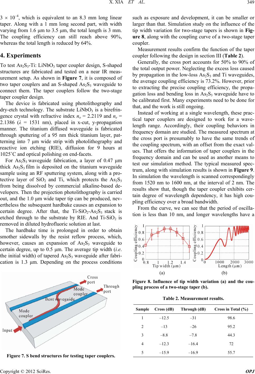 X. XIA ET AL. 349 3 10–4, which is equivalent to an 8.3 mm long linear taper. Along with a 1 mm long second part, with width varying from 1.6 μm to 3.5 μm, the total length is 3 mm. The coupling efficiency can still reach above 90%, whereas the total length is reduced by 64%. 4. Experiments To test As2S3-Ti: LiNbO3 taper coupler design, S-shaped structures are fabricated and tested on a near IR meas- urement setup. As shown in Figure 7, it is composed of two taper couplers and an S-shaped As2S3 waveguide to connect them. The taper couplers follow the two-stage taper coupler design. The device is fabricated using photolithography and dry-etch technology. The substrate LiNbO3 is a birefrin- gence crystal with refractive index no = 2.2119 and ne = 2.1386 (λ = 1531 nm), placed in x-cut, y-propagation manner. The titanium diffused waveguide is fabricated through sputtering of a 95 nm thick titanium layer, pat- terning into 7 μm wide strip with photolithography and reactive ion etching (RIE), diffusion for 9 hours at 1025˚C and optical polishing on end-facets. For As2S3 waveguide fabrication, a layer of 0.47 μm thick As2S3 film is deposited on the titanium waveguide sample using an RF sputtering system, along with a pro- tective layer of SiO2 and Ti, which protects the As2S3 from being dissolved by commercial alkaline-based de- velopers. Then the projection photolithography is carried out, and the 1.0 μm wide taper tip can be produced, nev- ertheless the subsequent hardbake causes an expansion to certain degree. After that, the Ti-SiO2-As2S3 stack is etched through to the substrate by RIE. And Ti-SiO2 is removed in diluted hydrofluoric solution at last. The hardbake time is prolonged in order to obtain smother sidewalls by the resist reflow process, which, however, causes an expansion of As2S3 waveguide to certain degree, up to 0.5 μm. The average tip width (i.e. the initial width) of tapered As2S3 waveguide after fabri- cation is 1.3 μm. Depending on the process conditions Figure 7. S bend structures for testing taper couplers. such as exposure and development, it can be smaller or larger than that. Simulation study on the influence of the tip width variation for two-stage tapers is shown in Fig- ure 8, along with the coupling curve of a two-stage taper coupler. Measurement results confirm the function of the taper coupler following the design in section III (Table 2). Generally, the cross port accounts for 50% to 90% of the total output power. Neglecting the excess loss caused by propagation in the low-loss As2S3 and Ti waveguides, the average coupling efficiency is 73.2%. However, prior to extracting the precise coupling efficiency, the propa- gation loss and bending loss in As2S3 waveguide have to be calibrated first. Many experiments need to be done for that, and the work is still ongoing. Instead of working at a single wavelength, these prac- tical taper couplers are designed to work for a wave- length range. Accordingly, their coupling behaviors in frequency domain are studied. The measured spectrum at the cross port is presumably to have the same trends of the coupling spectrum, with an offset from the exact val- ues. That offers the information of taper couplers in the frequency domain and can be used as another means to test our simulation method. The typical measured spec- trum, along with simulation results is shown in Figure 9. In simulation the wavelength is scanned correspondingly from 1520 nm to 1600 nm, at the interval of 2 nm. The results show that, though the taper coupler exhibits cer- tain degree of wavelength dependency, it has high cou- pling efficiency over a broad bandwidth. From the curve, we can see that the period of oscilla- tion is less than 10 nm, and longer wavelengths have a (a) (b) Figure 8. Influence of tip width variation (a) and the cou- pling process of a two-stage taper (b). Table 2. Measurement results. Sample Cross (dB)Through (dB) Cross in Total (%) 1 –12.5 –31 98.6 2 –13 –26 95.2 3 –8.8 –7.8 44.3 4 –12.3 –16.4 72 5 –15.9 –16.9 55.7 Copyright © 2012 SciRes. OPJ 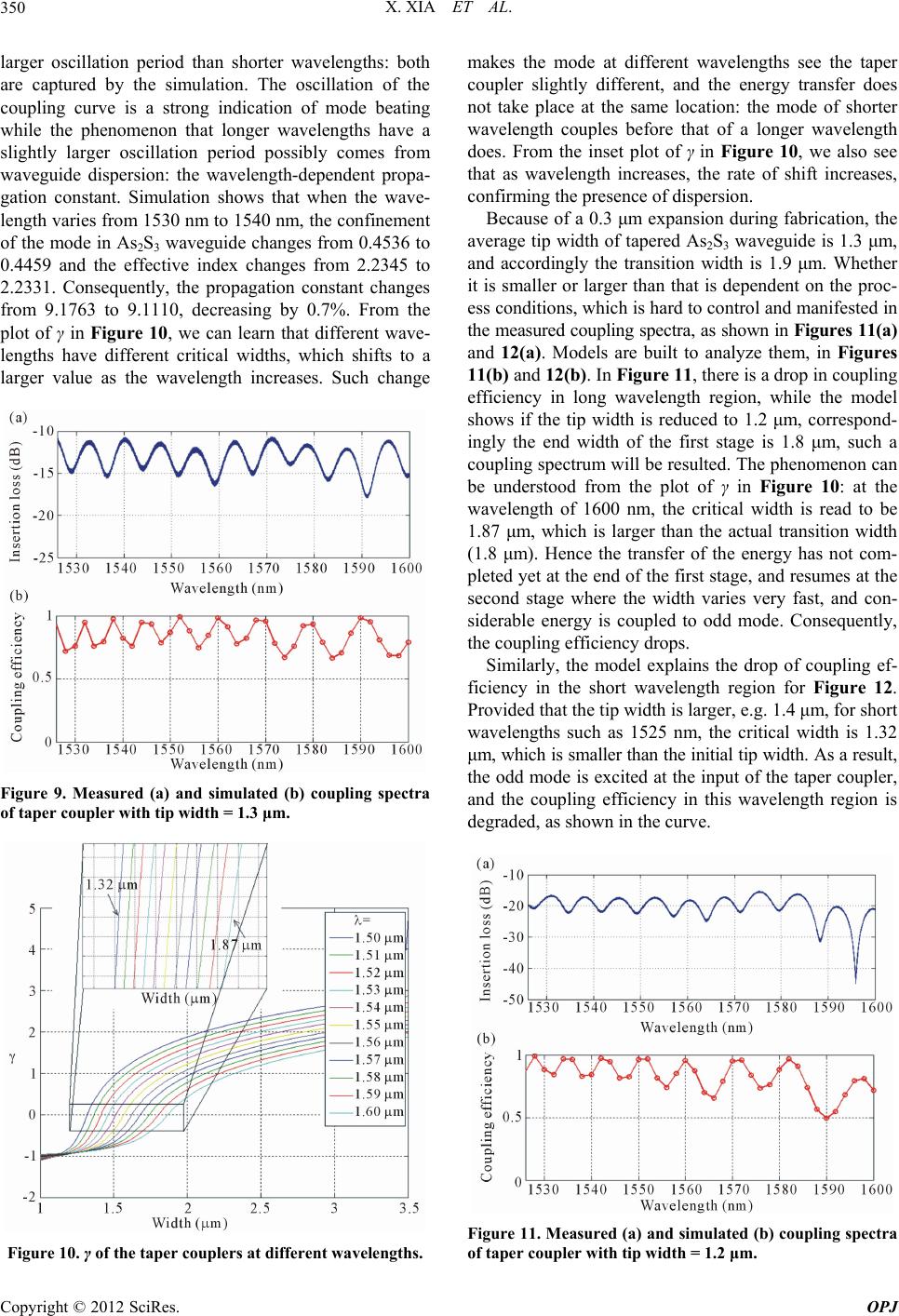 X. XIA ET AL. 350 larger oscillation period than shorter wavelengths: both are captured by the simulation. The oscillation of the coupling curve is a strong indication of mode beating while the phenomenon that longer wavelengths have a slightly larger oscillation period possibly comes from waveguide dispersion: the wavelength-dependent propa- gation constant. Simulation shows that when the wave- length varies from 1530 nm to 1540 nm, the confinement of the mode in As2S3 waveguide changes from 0.4536 to 0.4459 and the effective index changes from 2.2345 to 2.2331. Consequently, the propagation constant changes from 9.1763 to 9.1110, decreasing by 0.7%. From the plot of γ in Figure 10, we can learn that different wave- lengths have different critical widths, which shifts to a larger value as the wavelength increases. Such change Figure 9. Measured (a) and simulated (b) coupling spectra of taper coupler with tip width = 1.3 μm. Figure 10. γ of the taper couplers at different wavelengths. makes the mode at different wavelengths see the taper coupler slightly different, and the energy transfer does not take place at the same location: the mode of shorter wavelength couples before that of a longer wavelength does. From the inset plot of γ in Figure 10, we also see that as wavelength increases, the rate of shift increases, confirming the presence of dispersion. Because of a 0.3 μm expansion during fabrication, the average tip width of tapered As2S3 waveguide is 1.3 μm, and accordingly the transition width is 1.9 μm. Whether it is smaller or larger than that is dependent on the proc- ess conditions, which is hard to control and manifested in the measured coupling spectra, as shown in Figures 11(a) and 12(a). Models are built to analyze them, in Figures 11(b) and 12(b). In Figure 11, there is a drop in coupling efficiency in long wavelength region, while the model shows if the tip width is reduced to 1.2 μm, correspond- ingly the end width of the first stage is 1.8 μm, such a coupling spectrum will be resulted. The phenomenon can be understood from the plot of γ in Figure 10: at the wavelength of 1600 nm, the critical width is read to be 1.87 μm, which is larger than the actual transition width (1.8 μm). Hence the transfer of the energy has not com- pleted yet at the end of the first stage, and resumes at the second stage where the width varies very fast, and con- siderable energy is coupled to odd mode. Consequently, the coupling efficiency drops. Similarly, the model explains the drop of coupling ef- ficiency in the short wavelength region for Figure 12. Provided that the tip width is larger, e.g. 1.4 μm, for short wavelengths such as 1525 nm, the critical width is 1.32 μm, which is smaller than the initial tip width. As a result, the odd mode is excited at the input of the taper coupler, and the coupling efficiency in this wavelength region is degraded, as shown in the curve. Figure 11. Measured (a) and simulated (b) coupling spectra of taper coupler with tip width = 1.2 μm. Copyright © 2012 SciRes. OPJ 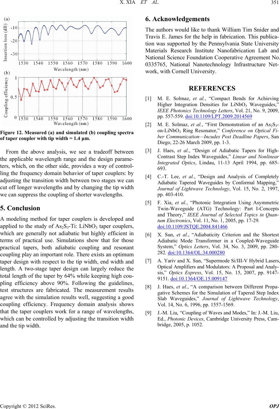 X. XIA ET AL. Copyright © 2012 SciRes. OPJ 351 6. Acknowledgements The authors would like to thank William Tim Snider and Travis E. James for the help in fabrication. This publica- tion was supported by the Pennsylvania State University Materials Research Institute Nanofabrication Lab and National Science Foundation Cooperative Agreement No. 0335765, National Nanotechnology Infrastructure Net- work, with Cornell University. REFERENCES [1] M. E. Solmaz, et al., “Compact Bends for Achieving Higher Integration Densities for LiNbO3 Waveguides,” IEEE Photonics Technology Letters, Vol. 21, No. 9, 2009, pp. 557-559. doi:10.1109/LPT.2009.2014569 [2] M. E. Solmaz, et al., “First Demonstration of an As2S3- on-LiNbO3 Ring Resonator,” Conference on Optical Fi- ber Communication—Incudes Post Deadline Papers, San Diego, 22-26 March 2009, pp. 1-3. Figure 12. Measured (a) and simulated (b) coupling spectra of taper coupler with tip width = 1.4 μm. [3] J. Haes, et al., “Design of Adiabatic Tapers for High- Contrast Step Index Waveguides,” Linear and Nonlinear Integrated Optics, Lindau, 11-13 April 1994, pp. 685- 693. From the above analysis, we see a tradeoff between the applicable wavelength range and the design parame- ters, which, on the other side, provides a way of control- ling the frequency domain behavior of taper couplers: by adjusting the transition width between two stages we can cut off longer wavelengths and by changing the tip width we can suppress the coupling of shorter wavelengths. [4] C.-T. Lee, et al., “Design and Analysis of Completely Adiabatic Tapered Waveguides by Conformal Mapping,” Journal of Lightwave Technology, Vol. 15, No. 2, 1997, pp. 403-410. [5] F. Xia, et al., “Photonic Integration Using Asymmetric Twin-Waveguide (ATG) Technology: Part I-Concepts and Theory,” IEEE Journal of Selected Topics in Quan- tum Electronics, Vol. 11, No. 1, 2005, pp. 17-29. doi:10.1109/JSTQE.2004.841466 5. Conclusion A modeling method for taper couplers is developed and applied to the study of As2S3-Ti: LiNbO3 taper couplers, which are generally not adiabatic but highly efficient in terms of practical use. Simulations show that for those practical tapers, both adiabatic coupling and resonant coupling play an important role. There exists an optimum taper design with respect to the tip width, end width and length. A two-stage taper design can largely reduce the total length of the taper by 64% while keeping high cou- pling efficiency above 90%. Following the guidelines, test structures are fabricated. The measurement results agree with the simulation results well, suggesting a good coupling efficiency. Frequency domain analysis shows that the taper couplers work for a range of wavelengths, which can be controlled by adjusting the transition width and the tip width. [6] X. Sun, et al., “Adiabaticity Criterion and the Shortest Adiabatic Mode Transformer in a Coupled-Waveguide System,” Optics Letters, Vol. 34, No. 3, 2009, pp. 280- 282. doi:10.1364/OL.34.000280 [7] A. Yariv and X. Sun, “Supermode Si/III-V Hybrid Lasers, Optical Amplifiers and Modulators: A Proposal and Analy- sis,” Optics Express, Vol. 15, No. 15, 2007, pp. 9147- 9151. doi:10.1364/OE.15.009147 [8] J. Haes, et al., “A comparison between Different Propa- gative Schemes for the Simulation of Tapered Step Index Slab Waveguides,” Journal of Lightwave Technology, Vol. 14, No. 6, 1996, pp. 1557-1569. [9] J.-M. Liu, “Coupling of Waves and Modes,” In: J.-M. Liu, Ed., Photonic Devices, Cambridge University Press, Cam- bridge, 2005, p. 1052.
|