Paper Menu >>
Journal Menu >>
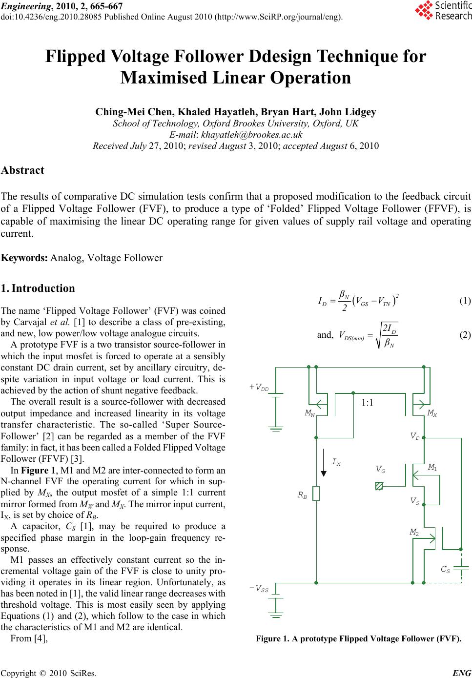 Engineering, 2010, 2, 665-667 doi:10.4236/eng.2010.28085 Published Online August 2010 (http://www.SciRP.org/journal/eng). Copyright © 2010 SciRes. ENG Flipped Voltage Follower Ddesign Technique for Maximised Linear Operation Ching-Mei Chen, Khaled Hayatleh, Bryan Hart, John Lidgey School of Technology, Oxford Brookes University, Oxford, UK E-mail: khayatleh@brookes.ac.uk Received July 27, 2010; revised August 3, 2010; accepted August 6, 2010 Abstract The results of comparative DC simulation tests confirm that a proposed modification to the feedback circuit of a Flipped Voltage Follower (FVF), to produce a type of ‘Folded’ Flipped Voltage Follower (FFVF), is capable of maximising the linear DC operating range for given values of supply rail voltage and operating current. Keywords: Analog, Voltage Follower 1. Introduction The name ‘Flipped Voltage Follower’ (FVF) was coined by Carvajal et al. [1] to describe a class of pre-existing, and new, low power/low voltage analogue circuits. A prototype FVF is a two transistor source-follower in which the input mosfet is forced to operate at a sensibly constant DC drain current, set by ancillary circuitry, de- spite variation in input voltage or load current. This is achieved by the action of shunt negative feedback. The overall result is a source-follower with decreased output impedance and increased linearity in its voltage transfer characteristic. The so-called ‘Super Source- Follower’ [2] can be regarded as a member of the FVF family: in fact, it has been called a Folded Flipped Voltage Follower (FFVF) [3]. In Figure 1, M1 and M2 are inter-connected to form an N-channel FVF the operating current for which in sup- plied by MX, the output mosfet of a simple 1:1 current mirror formed from MW and MX. The mirror input current, IX, is set by choice of RB. A capacitor, CS [1], may be required to produce a specified phase margin in the loop-gain frequency re- sponse. M1 passes an effectively constant current so the in- cremental voltage gain of the FVF is close to unity pro- viding it operates in its linear region. Unfortunately, as has been noted in [1], the valid linear range decreases with threshold voltage. This is most easily seen by applying Equations (1) and (2), which follow to the case in which the characteristics of M1 and M2 are identical. From [4], 2 N DGSTN β IVV 2 (1) and, D DS(min) N 2I V β (2) Figure 1. A prototype Flipped Voltage Follower (FVF). RB +VDD -VSS MW MX M1 M2 VG 1:1 IX VD VS CS 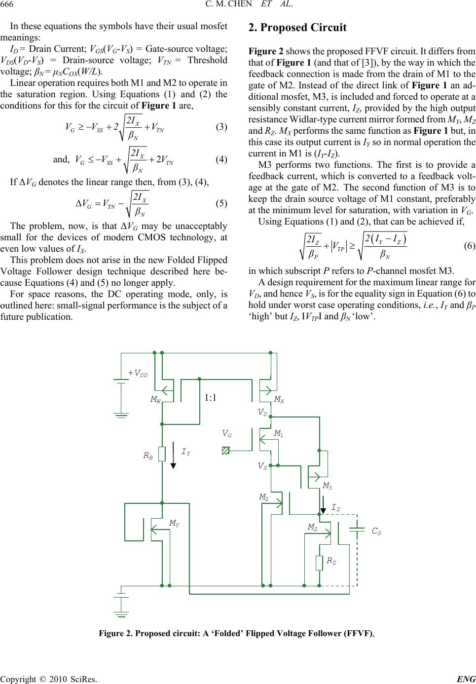 C. M. CHEN ET AL. Copyright © 2010 SciRes. ENG 666 In these equations the symbols have their usual mosfet meanings: ID = Drain Current; VGS(VG-VS) = Gate-source voltage; VDS(VD-VS) = Drain-source voltage; VTN = Threshold voltage; βN = μNCOX(W/L). Linear operation requires both M1 and M2 to operate in the saturation region. Using Equations (1) and (2) the conditions for this for the circuit of Figure 1 are, X GSS TN N 2I VV2 V β (3) and, 2 X GSS TN N 2I VV V β (4) If ΔVG denotes the linear range then, from (3), (4), X GTN N 2I VV β (5) The problem, now, is that ΔVG may be unacceptably small for the devices of modern CMOS technology, at even low values of IX. This problem does not arise in the new Folded Flipped Voltage Follower design technique described here be- cause Equations (4) and (5) no longer apply. For space reasons, the DC operating mode, only, is outlined here: small-signal performance is the subject of a future publication. 2. Proposed Circuit Figure 2 shows the proposed FFVF circuit. It differs from that of Figure 1 (and that of [3]), by the way in which the feedback connection is made from the drain of M1 to the gate of M2. Instead of the direct link of Figure 1 an ad- ditional mosfet, M3, is included and forced to operate at a sensibly constant current, IZ, provided by the high output resistance Widlar-type current mirror formed from MY, MZ and RZ. MX performs the same function as Figure 1 but, in this case its output current is IY so in normal operation the current in M1 is (IY-IZ). M3 performs two functions. The first is to provide a feedback current, which is converted to a feedback volt- age at the gate of M2. The second function of M3 is to keep the drain source voltage of M1 constant, preferably at the minimum level for saturation, with variation in VG. Using Equations (1) and (2), that can be achieved if, YZ Z TP PN 2I I 2I V ββ (6) in which subscript P refers to P-channel mosfet M3. A design requirement for the maximum linear range for VD, and hence VS, is for the equality sign in Equation (6) to hold under worst case operating conditions, i.e., IY and βP ‘high’ but IZ, ΙVTPΙ and βN ‘low’. Figure 2. Proposed circuit: A ‘Folded’ Flipped Voltage Follower (FFVF). RB +VDD MW MX M1 M2 VG RZ CS MZ M3 MY 1:1 VD VS IY I Z 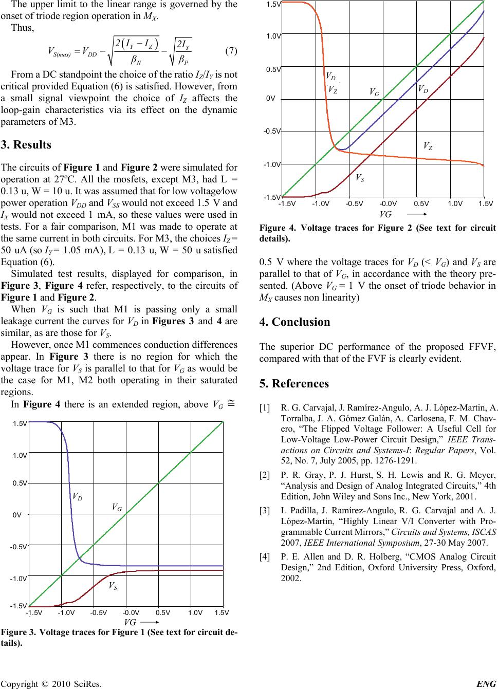 Copyright © 2010 SciRes. ENG The upper limit to the linear range is governed by the onset of triode region operation in MX. Thus, YZ Y S(max) DD N P 2I I2I VV β β (7) From a DC standpoint the choice of the ratio IZ/IY is not critical provided Equation (6) is satisfied. However, from a small signal viewpoint the choice of IZ affects the loop-gain characteristics via its effect on the dynamic parameters of M3. 3. Results The circuits of Figure 1 and Figure 2 were simulated for operation at 27ºC. All the mosfets, except M3, had L = 0.13 u, W = 10 u. It was assumed that for low voltage⁄low power operation VDD and VSS would not exceed 1.5 V and IX would not exceed 1 mA, so these values were used in tests. For a fair comparison, M1 was made to operate at the same current in both circuits. For M3, the choices IZ = 50 uA (so IY = 1.05 mA), L = 0.13 u, W = 50 u satisfied Equation (6). Simulated test results, displayed for comparison, in Figure 3, Figure 4 refer, respectively, to the circuits of Figure 1 and Figure 2. When VG is such that M1 is passing only a small leakage current the curves for VD in Figures 3 and 4 are similar, as are those for VS. However, once M1 commences conduction differences appear. In Figure 3 there is no region for which the voltage trace for VS is parallel to that for VG as would be the case for M1, M2 both operating in their saturated regions. In Figure 4 there is an extended region, above VG Figure 3. Voltage traces for Figure 1 (See text for circuit de- tails). Figure 4. Voltage traces for Figure 2 (See text for circuit details). 0.5 V where the voltage traces for VD (< VG) and VS are parallel to that of VG, in accordance with the theory pre- sented. (Above VG = 1 V the onset of triode behavior in MX causes non linearity) 4. Conclusion The superior DC performance of the proposed FFVF, compared with that of the FVF is clearly evident. 5. References [1] R. G. Carvajal, J. Ramírez-Angulo, A. J. López-Martin, A. Torralba, J. A. Gómez Galán, A. Carlosena, F. M. Chav- ero, “The Flipped Voltage Follower: A Useful Cell for Low-Voltage Low-Power Circuit Design,” IEEE Trans- actions on Circuits and Systems-I: Regular Papers, Vol. 52, No. 7, July 2005, pp. 1276-1291. [2] P. R. Gray, P. J. Hurst, S. H. Lewis and R. G. Meyer, “Analysis and Design of Analog Integrated Circuits,” 4th Edition, John Wiley and Sons Inc., New York, 2001. [3] I. Padilla, J. Ramírez-Angulo, R. G. Carvajal and A. J. López-Martin, “Highly Linear V/I Converter with Pro- grammable Current Mirrors,” Circuits and Systems, ISCAS 2007, IEEE International Symposium, 27-30 May 2007. [4] P. E. Allen and D. R. Holberg, “CMOS Analog Circuit Design,” 2nd Edition, Oxford University Press, Oxford, 2002. VG -1.5V -1.0V -0.5V -0.0V 0.5V 1.0V1.5V VG VD VS 0V -1.5V -1.0V -0.5V 0.5V 1.0V 1.5V VG -1.5V -1.0V -0.5V -0.0V 0.5V 1.0V 1.5V -1.5V -1.0V -0.5V 0V 0.5V 1.0V 1.5V VD, VD VG VS VZ VZ VD VG V S VG VD VD VZVG VZ VS VG |