Journal of Modern Physics, 2012, 3, 1550-1555
http://dx.doi.org/10.4236/jmp.2012.310191 Published Online October 2012 (http://www.SciRP.org/journal/jmp)
Theory of Conductivity in Semiconducting Single-Wall
Carbon Nanotubes
Shigeji Fujita1, Salvador Godoy2, Akira Suzuki3*
1Department of Physics, University at Buffalo, Buffalo, USA
2Departamento de Física, Facultad de Ciencias, Universidad Nacional Autónoma de México, Mexico City, Mexico
3Department of Physics, Faculty of Science, Tokyo University of Science, Shinjuku-ku, Japan
Email: *asuzuki@rs.kagu.tus.ac.jp
Received August 13, 2012; revised September 16, 2012; accepted September 23, 2012
ABSTRACT
The conduction of a single-wall carbon nanotube depends on the pitch. If there are an integral number of carbon hexa-
gons per pitch, then the system is periodic along the tube axis and allows “holes” (not “electrons”) to move inside the
tube. This case accounts for a semiconducting behavior with the activation energy of the order of around 3 meV. There
is a distribution of the activation energy since the pitch and the circumference can vary. Otherwise nanotubes show me-
tallic behaviors (significantly higher conductivity). “Electrons” and “holes” can move in the graphene wall (two dimen-
sions). The conduction in the wall is the same as in graphene if the finiteness of the circumference is disregarded. Coo-
per pairs formed by the phonon exchange attraction moving in the wall is shown to generate a temperature-independent
conduction at low temperature (3 - 20 K).
Keywords: Semiconducting SWNT; Cartesian Unit Cell Model; Cooper Pair; Bloch Electron Dynamics
1. Introduction
Iijima [1] found after his electron diffraction analysis
that carbon nanotubes ranging 4 to 30 nanometers (nm)
in diameter have helical multi-walled structures. Single-
wall nanotube (SWNT) has about one nanometer in di-
ameter and micrometers (μm) in length. Ebbesen et al. [2]
measured the electrical conductivity
of individual
carbon nanotubes and found that
varies depending of
the temperature T, the tube radius r and the pitch p. Ex-
periments show that SWNT can be either semiconducting
or metallic, depending on how they are rolled up from
the graphene sheets [3]. In the present work we shall
present a microscopic theory of the electrical conductiv-
ity of semiconducting SWNT, starting with a graphene
honeycomb lattice, developing a Bloch electron dynam-
ics based on a rectangular cell model [4], and using ki-
netic theory. A SWNT can be formed by rolling a gra-
phene sheet into a circular cylinder. The graphene which
forms a honeycomb lattice is intrinsically anisotropic as
we shall explain it in more detail later in Section 2. Mo-
riyama et al. [5] fabricated 12 SWNT devices from one
chip, and observed that two of the SWNT samples are
semiconducting and the other 10 are metallic. The semi-
conducting SWNT samples show an activated-state tem-
perature behavior. That is, the resistance decreases with
increasing temperature. Why are there two sets of sam-
ples showing very different behavior? The answer to this
question is as follows.
The line passing the centers of the nearest-neighbor
carbon hexagons forms a helical line around the nano-
tube with a pitch p and a radius r.
In Figure 1(a), a section of the circular tube with a
pitch p is drawn. Its unrolled plane is shown in (b). The
circumference likely contains an integral number
m of the carbon hexagons (units). The pitch p, however,
may or may not contain an integral number n of units. In
the fabrication process the pitch is not controlled. In the
first alternative, the nanotube is periodic with the period
p along the tube axis. Then, there is a one-dimensional
(1D) k-vector along the tube. A “hole” which has a posi-
tive charge +e and a size of a unit ring of height p and
radius r can go through inside the positively charged
carbon wall. An “electron” having a negative charge e
and a similar size is attracted by the carbon wall, and
hence it cannot go straight inside the wall. Thus, there
should be an extra “hole” channel current in a SWNT.
Moriyama et al. [5] observed a “hole”-like current after
examining the gate voltage effect. The system should
have the lowest energy if the unit ring contains an integer
set
2πr
,mn of carbon hexagons, which may be attained
*Corresponding author.
C
opyright © 2012 SciRes. JMP
S. FUJITA ET AL. 1551
(a) (b)
Figure 1. (a) A section circular tube wall with a radius r and
a pith p; (b) Its unrolled plane.
after annealing at high temperatures. This should happen
if the tube length is comparable with the circumference.
The experimental tube length is much greater than the
circumference, and the pitch angle can be varied con-
tinuously. The set of irrational numbers is greater in car-
dinality than the set of rational numbers. Then, the first
case in which the unit contains an integer set
,mn of
hexagons must be the minority. This case then generates
a semiconducting transport behavior. We shall show later
that the transport requires an activation energy. Fujita
and Suzuki [4] showed that the “electrons” and “holes”
must be activated based on the rectangular unit cell mod-
el for graphene.
Saito, Dresselhaus and Dresselhaus [3] state that a
SWNT is characterized by two integer indices
,mn
mn
ˆˆˆ
,
,
for example, for an armchair nanotube whereas
for a zigzag nanotube. If is a multiple of
3, then a SWNT is metallic. They then argued that ap-
proximately one third of the SWNT are metallic, and the
other two thirds are semiconducting. This model is in
variance with the experimental observation by Moriyama
et al. [5], where the majority of SWNT is metallic. We
must look for a different classification scheme.
0mnm
If a SWNT contains an irrational number of carbon
hexagons, which happens more often, then the system
does not allow a conduction along the tube axis. The
system is still conductive since the conduction electrons
(“electrons”, “holes”) can go through in the tube wall.
This conduction is two-dimensional (2D), opposed to 1D,
as can be seen in the unrolled configuration, which is
precisely the graphene honeycomb lattice. This means
that the conduction in the carbon wall should be the same
as the conduction in graphene if the effect of the finite-
ness of the radius is neglected.
We consider graphene in Section 2. The current band
theory of the honeycomb crystal is based on the Wigner-
Seitz (WS) cell model [3,6]. The model applied to gra-
phene predict a gapless semiconductor, which is not ob-
served. The WS model [6] is suitable for the study of the
ground-state energy of the crystal. To describe the Bloch
electron dynamics [7] a new theory based on the Carte-
sian unit cell not matching with the natural triangular
crystal axes must be used. Also the phonons can be dis-
cussed using Cartesian coordinate-systems, not with the
triangular coordinate-systems. The conduction electron
moves as a wave packet formed by the Bloch waves as
pointed out by Ashcroft and Mermin in their book [7].
This picture is fully incorporated in our new theoretical
model.
2. Graphene
We consider a graphene, in which carbon ions (C+) oc-
cupy a 2D honeycomb lattice, See Figure 2. The normal
current carriers are “electrons” and “holes”. Following
Ashcroft and Mermin [7], we adopt the semiclassical
model of electron dynamics in solids. “Electrons”
(“holes”) are defined as quasi-electrons which move
counterclockwise (clockwise) viewed from the tip of the
applied magnetic field. In the semiclassical (wave packet)
theory, it is necessary to introduce a k-vector:
x
xyyzz
kke keke
ˆ
(1)
where
x
eˆ
,
y
eˆ
,
z
e are the Cartesian orthonormal vec-
tors, since the k-vectors are involved in the semi-
classical equation of motion:

d,
dq
t

k
kEvB

q
(2)
where is the charge of a conduction electron, and
E
and are the electric and magnetic fields, respectively.
The vector
B
1
vk

=

k
z
(3)
is the electron velocity, where is the energy.
The 2D crystals such as graphene can also be treated
similarly, only the -component being dropped. The
choice of the Cartesian axes and the unit cell is obvious
for the cubic crystals. We must choose an orthogonal unit
cell also for the honeycomb lattice, as demonstrated
below.
Graphene forms a 2D honeycomb lattice. The WS unit
cell is a rhombus shown in Figure 2(a).
Vr is lattice-periodic: The potential energy

,
mn
VVrR r
12
,
mn mn
(4)
where
Raa (5)
is a Bravais vector with the primitive vectors
,aa
12
and integers
,mn
r. In the field theoretical formulation
the field point is given by
Copyright © 2012 SciRes. JMP
S. FUJITA ET AL.
1552
,
mn

rrR
r
(6)
where is the point defined within the standard unit
cell. Equation (4) describes the 2D lattice periodicity
but does not establish the k-space, which is explained
below.
To see this clearly, we first consider an electron in a
simple square (sq) lattice. The Schrödingier wave equa-
tion is
 
2
2
*
i
 
sq
2V
tm

 
rrrr

0
mn
R
ˆˆ,
nstant)
x y
mana ee



0
sq
mn Vr
. (7)
The Bravais vector for the sq lattice is

0
(lattice co
mnx y
a
Raamn (8)
The system is lattice periodic:
sq
VrR . (9)
If we choose a set of Cartesian coordinates
,
x
y
along the sq lattice, then the Laplacian term in Equation
(7) is given by
 
22
22 ,.
2,
x
yxy
xy




Vr


 (10)
If we choose a periodic square boundary with the side
length Na, N = integer, then there are 2D Fourier trans-
forms and k-vectors.
We now go back to the original graphene system. If
we choose the x-axis along either a1 or a2, then the po-
tential energy field is periodic in the x-direction
but it is aperiodic in the y-direction. For an infinite lattice
the periodic boundary is the only acceptable boundary
condition for the Fourier transformation. Then, there is
no 2D k-space spanned by 2D k-vectors. If we omit the
kinetic energy term, then we can still use Equation (4)
and obtain the ground state energy (except the zero point
energy).
We now choose the orthogonal unit cell shown in Fig-
ure 2(b). The unit has side lengths
1020
3, 3,baba
a
(11)
where 0 is the nearest neighbor distance between two
C’s. The unit cell has four (4) C’s. The system is lattice-
periodic in the x- and y-directions, and hence there are
2D k-space.
The “electron” (“hole”) is defined as a quasi-electron
which has an energy higher (lower) than the Fermi en-
ergy
F
and “electron” (“hole”) are excited on the posi-
tive (negative) side of the Fermi surface with the conven-
tion that the positive normal vector at the surface points
in the energy-increasing direction.
The “electron” (wave packet) may move up or down
along the y-axis to the neighboring unit cells passing
(a) (b)
Figure 2. (a) WS unit cell, rhombus (dotted lines) for gra-
phene; (b) The orthogonal unit cell, rectangle (dotted lines).
over one C+. The positively charged C+ acts as a wel-
coming (favorable) potential valley for the negatively
charged “electron”, while the same C+ act as a hindering
potential hill for the positively charged “hole”. The
“hole”, however, can move horizontally along the x-axis
without meeting the hindering potential hills. Thus the
easy channel directions for the “elections” (“holes”) are
along the y- (x-) axes.
Let us consider the system (graphene) at 0 K. If we put
an electron in the crystal, then the electron should occupy
the center O of the Brillouin zone, where the lowest en-
ergy lies. Additional electrons occupy points neighboring
the center O in consideration of Pauli’s exclusion princi-
ple. The electron distribution is lattice-periodic over the
entire crystal in accordance with the Bloch theorem [8].
Carbon (C) is a quadrivalent metal. The first few low-
lying energy bands are completely filled. The uppermost
partially filled bands are important for transport proper-
ties discussion. We consider such a band. The (2D) Fer-
mi surface, which defines the boundary between the
filled and unfilled k-space (area) is not a circle since the
x-y symmetry is broken (bc
). The “electron” effective
mass is lighter in the direction [110] than perpendicular
to it. Hence the electron motion is intrinsically anisot-
ropic. The negatively charged “electron” is near the posi-
tive ions C+. Hence, the gain in the Colulomb interaction
is greater for “electron”. Thus, the “electrons” are the
majority carriers at zero gate voltage. That is, the system
has two different masses and it is intrinsically anisotropic.
If the electron number is raised by the gate voltage ap-
plied perpendicular to the plane, then the Fermi surface
more quickly grows in the easy-axis (y-) direction than in
the x-direction. The Fermi surface must approach the
Brillouin boundary at right angles because of the inver-
sion symmetry possessed by honeycomb lattice [9]. Then
at a certain voltage, a “neck” Fermi surface must be de-
veloped.
The same easy channels in which the “electron” runs
with a small mass, may be assumed for other hexagonal
directions, [011] and [101]. The currents run in the three
channels
, and
101 . The total 110110 ,011
Copyright © 2012 SciRes. JMP
S. FUJITA ET AL. 1553
current (magnitude) along the field direction
is pro-
portional to [10]


2
channels
22 2
cos ,
cos cos2π3cos2π332.

 
 
(12)
E3meV
Note that this current does not depend on the angle
between the field direction (
) and the channel current
direction (). More detailed discussion can be found in
ref. [10]. Hence, the graphene does not show anisotropy
in the conductivity.
12
<
We have seen earlier that the “electron” and “hole”
have different internal charge distributions and therefore
have different effective masses. Which carriers are easier
to be activated or excited? The “electron” is near the pos-
itive ions and the “hole” is farther away from the ions.
Hence, the gain in the Coulomb interaction is greater for
the “electron”. That is, the “electrons” are more easily
activated (or excited). The presence of the welcoming C+
ions in the channel direction also enhances this inequal-
ity.
We may represent the activation energy difference by
[6]
.
(13)
The thermally-activated (or excited) electron densities
are given by


B
p ,
j
kT

=1j
ex
jj
nT n (14)
where and 2 represent the “electron” and “hole”,
respectively. The prefactor
j
n is the density at high-
temperature limit.
3. SWNT
Let us consider the long SWNT rolled with a graphene
sheet. The charge may be transported by the channeling
“electrons” and “holes” in the graphene wall. But the
“holes” within the wall can also contribute to the charge
transport. Because of this extra channel inside the carbon
nanotube, “holes” are likely to be the majority carriers in
nanotubes although “electrons” are the dominant carriers
in graphene. Moriyama et al. [5] studied the electrical
transport in semiconducting SWNT in the temperature
range 2.6 - 200 K, and found from the filed (gate voltage)
effect that the carriers are “hole”-like. Their data are re-
produced in Figure 3.
The conductivity depends on the pitch of the SWNT.
The helical line is defined as the line passing the nearest
neighbors of the C-hexagons. The helical angle
is the
angle between the helical line and the tube axis. The
degree of helicity may be defined as
h
cos .h
(15)
For a macroscopically large graphene the conductivity
Figure 3. Log-scale plot of the currents in semiconducting
SWNT as a function of inverse temperature after Mori-
yama et al. [5].
is isotropic as we saw in Section 2. The conductivity
in (semiconducting) SWNT depends on this helicity .
This is a kind of a finite size effect. The circumference is
finite while the tube length is macroscopic.
h
In a four-valance-electron conductor such as graphene
all electrons are bound to ions at 0 K, and there is no
conduction. If a “hole” having the charge +e and the size
of a unit ring is excited, then this “hole” can move along
the tube axis with the activation energy 3
and the ef-
fective mass 3. Both m3
and depend on the ra-
dius and the pitch. 3
m
m
We are now ready to discuss the conductivity of se-
miconducting SWNT. There are four currents carried by
1) “Electrons” moving in the graphene wall with the
mass 1 and the density

11B
expnkT
, running in
the channels .
110
m2) “Holes” moving in the graphene wall with the mass
2 and the density

22B
expnkT
, running in the
channels 100 m
.
3) “Holes” moving with the mass 3 and the density
expnkT
33B
, running in the tube-axis direction. The
activation (or excitation) energy 3
and the effective
mass vary with the radius and the pitch.
3
4) Cooper pairs (pairons) formed by the phonon-
exchange attraction, which move in the graphene wall.
m
In actuality, one of the currents may be dominant, and
be observed.
In the normal Ohmic conduction due to the conduction
electrons the resistance is proportional to the sample
(tube) length. Then, the conductivity
is given by the
Drude formula:
22
**
1,
nq nq
mm


*
,em
(16)
where q is the carrier charge the effective
Copyright © 2012 SciRes. JMP
S. FUJITA ET AL.
1554
mass, n the carrier density, and
the relaxation (colli-
sion) time. The relaxation rate 1
Γ
Γ

ph .T
Γ
is the inverse of
the relaxation time. If the impurities and phonons are
scatterers, then the rate is the sum of the impurity
scattering rate
and the phonon scattering rate
: imp

imp

ph T
(17)
The impurity scattering rate imp is temperature-
independent and the phonon scattering rate
ΓT
T
 
above2K
Γ
ph is
temperature -dependent. The phonon scattering rate
is linear in above around 2 K:
T
Taa


ph T

ph T
Γ

ph
Γconstant,,T
nT
. (18)
The temperature dependence should arise from the
carrier density and the phonon scattering rate
. Writing the T-dependence explicitly, we obtain
from Equations (14)-(18)
2
*
=e
B
imp
1
Γ
kT
j
j
j
naT
33meV
.
(19)
j
e
m
Moriyama et al. [5] used the Arrhenius plot for the
data above 20 K and obtained the activation energy
.
n
(20)
By studying the field (gate voltage) effect, the carriers
were found to be “hole”-like. Thus, the major currents
observed can be interpreted in terms of the “holes” mov-
ing within the tube wall.
This “hole” axial transport depends on the unit ring
containing hexagons. Since the pitch and the cir-
cumference have distributions, the activation energy 3
m
should also have a distribution. Hence the obtained value
in Equation (20) must be regarded as the averaged value.
Liu et al. [10] systematically measured the resistance
of SWNT under hydrostatic pressures, and fitted
their data by using 2D variable range hopping (vrh)
theoretical formula [11]:

T


13
00
exp ,TT
0525 KT
T

(21)
where
(22)
is a fit (temperature) parameter and 0
a (resistance)
parameter. Mott’s vrh theory [12] is applicable when
highly random disorders exist in the system. An individ-
ual SWNT (annealed) is unlikely to have such random-
ness. We take a different view here. The scatterings are
due to impurities and phonons. But carriers (“holes”)
have a distribution in the unit cell size. Hence the distri-
bution of the activation energy introduces the flattening
of the Arrhenius slope by the factor 1/3. Compare Equa-
tion (21) and Equation (14).
The “hole” size is much greater than the usually as-
sumed atomic impurity size and the phonon size, which
are of the order of the lattice constant. This size mismatch
may account for a ballistic charge transport observed by
Frank et al. [13] and others [14]. More careful studies are
required to establish the cause of the ballisticity.
We now go back to the data shown in Figure 3. Below
20 K the currents observed are very small and they ap-
pear to approach a constant in the low temperature limit
(large 1
T
limit). These currents, we believe, are due to
the Cooper pairs.
The Cooper pairs (pairons) move in 2D with the linear
dispersion relation [15]:

,
j
cp

(23)


F
2π,
j
j
cv
(24)
where
F
j
v is the Fermi velocity of the “electron” (j = 1)
[“hole” (j = 2)].
Consider first “electron”-pairs. The velocity v is given
by (omitting superscript)
or ,
x
xx
p
p
vc
pp p




vp (25)
where
22
.
x
y
ppp (26)
The equation of motion along the E-field (x-) di-
rection is
,
x
pqE
t
q
(27)
is the charge 2e
where
of a pairon. The solution
of Equation (27) is given by

0,
xx
pqEtp


0
(28)
where
x
p is the initial momentum component. The
current density
p
jq is calculated from (charge
) ×
(number density
p
n) × (average velocity v). The av-
erage velocity v is calculated by using Equations (25)
and (28) with the assumption that the pair is accelerated
only for the collision time
. We then obtain

2
pp pp
1.
c
jqnvqncqEqnE
pp
 
 

(29)
For stationary currents, the pairon density np is given
by the Bose distribution function f
p
:
 
1
pB
exp1 ,
pp
nf kT

 
(30)
e
is the fugacity. Integrating the current
p
where j
pjE
over all 2D -space, and using Ohm’s law
we
obtain for the conductivity
:


222 1
2πd.
p
qcpp f

(31)
Copyright © 2012 SciRes. JMP
S. FUJITA ET AL.
Copyright © 2012 SciRes. JMP
1555

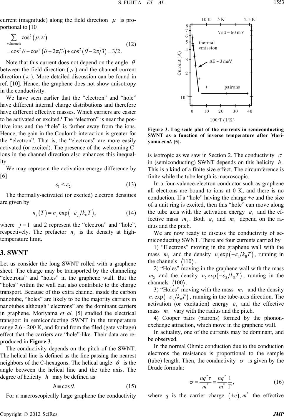
In the temperature ranging between 2 and 20 K we
may assume the Boltzmann distribution function for
p
f
:
 
Bp
exp
p.
f
kT


1
=aT
p
(32)
We assume that the relaxation time arises from the
phonon scattering so that , see Equations
(16)-(18). After performing the -integration we obtain
2
B
2
2,
π
ek e
a
(33)
which is temperature-independent. If there are “elec-
trons” and “hole” pairs, they contribute additively to the
conductivity. These pairons should undergo a Bose-Ein-
stein condensation at a temperature lower than 2.2 K. We
predict a superconducting state at lower temperatures.
4. Summary and Discussion
A SWNT is likely to have an integral number of carbon
hexagons around the circumference. If each pitch con-
tains an integral number of hexagons, then the system is
periodic along the tube axis, and “holes” (and not “elec-
trons”) can move along the tube axis. The system is se-
miconducting with an activation energy 3
. This energy
3
has a distribution since both pitch and circumference
have distributions. The pitch angle is not controlled in
the fabrication processes. There are more numerous cases
where the pitch contains an irrational numbers of hexa-
gons. In these cases the system shows a metallic behavior
experimentally [16].
In the process of arriving at our main conclusion we
have uncovered the following results.
1) “Electrons” and “holes” can move in 2D in the car-
bon wall in the same manner as in graphene.
2) For a metallic SWNT 1) implies that the conduction
in the wall shows no pitch dependence.
3) The Cooper pairs are formed in the wall. They
should undergo Bose-Einstein condensation at lower
temperature, exhibiting a superconducting state.
A metallic SWNT will be treated separately.
REFERENCES
[1] S. Iijima, “Helical Microtubules of Graphitic Carbon,”
Nature, Vol. 354, 1991, pp. 56-58. doi:10.1038/354056a0
[2] T. W. Ebbesen, H. J. Lezec, H. Hiura, J. W. Bennet , H. F.
Ghaemi and T. Thio, “Electrical Conductivity of Individ-
ual Carbon Nanotubes,” Nature, Vol. 382, 1996, pp. 54-
56. doi:10.1038/382054a0
[3] R. Saito, G. Dresselhaus and M. S. Dresselhaus, “Physi-
cal Properties of Carbon Nanotubes,” Imperial College
Press, London, 1998, pp. 35-58.
doi:10.1142/9781860943799_0003
[4] S. Fujita and A. Suzuki, “Theory of Temperature De-
pendence of the Conductivity in Carbon Nanotubes,”
Journal of Applied Physics, Vol. 107, 2010, Article ID:
013711. doi:10.1063/1.3280035
[5] S. Moriyama, K. Toratani, D. Tsuya, M. Suzuki, Y. Ao-
yagi and K. Ishibashi, “Electrical Transport in Semicon-
ducting Carbon Nanotubes,” Physica E, Vol. 24, No. 1-2,
2004, pp. 46-49. doi:10.1016/j.physe.2004.04.022
[6] E. Wigner and F. Seitz, “On the Constitution of Metallic
Sodium,” Physical Review, Vol. 43, No. 10, 1933, pp.
804-810. doi:10.1103/PhysRev.43.804
[7] N. W. Ashcroft and N. D. Mermin, “Solid State Physics,”
Saunders, 1976, pp. 91-93, 217, 228, 229.
[8] F. Bloch, “Über die Quantenmechanik der Elektronen in
Kristallgittern,” Z eit Physik, Vol. 52, 1928, pp. 555-599.
[9] S. Fujita and K. Ito, “Quantum Theory of Conducting
Matter,” Springer, New York, 2007, pp. 85-90,106-107.
doi:10.1007/978-0-387-74103-1
[10] S. Fujita, A. Garcia, D. O’Leyar, S. Watanabe and T.
Burnett, “On the Conductance of a Lattice-Like Net-
work,” Journal of Physics and Chemistry of Solids, Vol.
50, No. 1, 1989, pp. 27-31.
doi:10.1016/0022-3697(89)90468-X
[11] B. Liu, B. Sundqvist, O. Andersson, T. Wågberg, E. B.
Nyeanchi, X.-M. Zhu and G. Zou, “Electric Resistance of
Single-Walled Carbon Nanotubes under Hydrostatic
Pressure,” Solid State Communications, Vol. 118, No. 1,
2001, pp. 31-36. doi:10.1016/S0038-1098(01)00034-5
[12] N. F. Mott, “Conduction in Non-Crystalline Materials,”
Oxford University Press, Oxford, 1987.
[13] S. Frank, P. Poncharal, Z. I. Wang and W. A. de Heer,
“Carbon Nanotube Quantum Resistors,” Science, Vol.
280, No. 5370, 1998, pp. 1744-1746.
doi:10.1126/science.280.5370.1744
[14] A. Javey, J. Guo, Q. Wang, M. Lundstrom and H. Dai,
“Ballistic Carbon Nanotube Field-Effect Transistors,”
Nature, Vol. 424, 2003, pp. 654-657.
doi:10.1038/nature01797
[15] S. Fujita, K. Ito and S. Godoy, “Quantum Theory of
Conducting Matter: Superconductivity,” Springer, New
York, 2009, pp. 77-79.
[16] S. J. Tans, M. H. Devoret, H. Dai, A. Thess, R. E. Smal-
ley, L. J. Geerligs and C. Dekker, “Individual Single-Wall
Carbon Nanotubes as Quantum Wires,” Nature, Vol. 386,
1997, pp. 474-477. doi:10.1038/386474a0