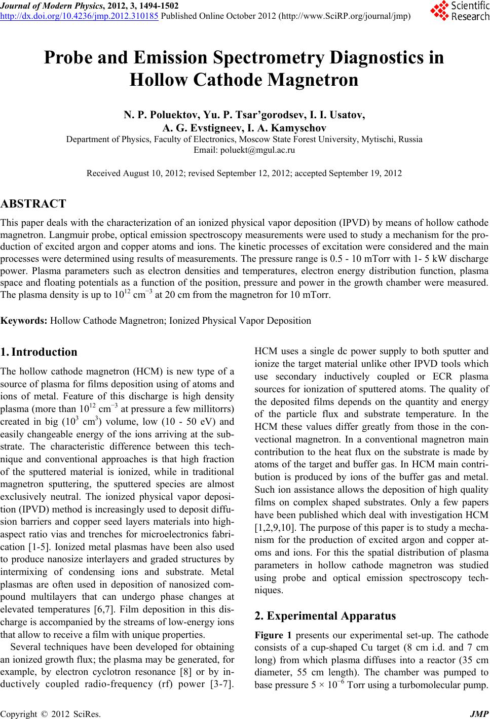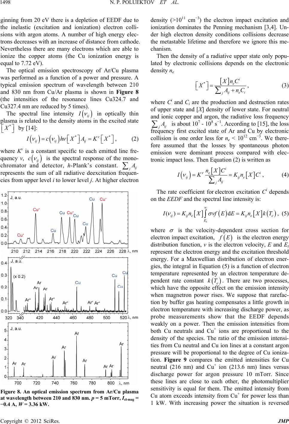
N. P. POLUEKTOV ET AL. 1501
2
*
Cu ,Cu
2
Cu diff
Cu ,Cu
Cu ,Cu
32
Cu
,Cu ,Cu
Cu ,CuCu ,Cu
Cu
CuCu
Ar
Ar Ar
e
eD
ee
e
DD
eee
e
ee
DD
eeeee
e
n
In
nk
n
nk nk
nn
nk nknk k
e
(27)
The copper ion diffusion term Cu
D
is much more
than total destructive (including double ionization) term
,Cu
ee
nk
. So that
*
Cu e
2
n
(28)
Thus, from the intensity variation of Cu and Cu+ spec-
tral lines with magnetron power, it is deduced that the
dominant loss term are electron ionization for the copper
atoms and diffusion for the copper ions.
In our model we neglect the influence of metastable
states of Cu and Ar atoms. Our measurements of the ab-
sorption coefficient of the line Cu510.6 nm shown that
density of the metastable level 2D5/2 is of an order less
than density of the ground level. From the absorption
coefficient of Ar696.5 and Ar811.5 nm lines we calcu-
lated density of metastable Ar level s5 (Pashen notation).
The Ar metastable state density was found in the range of
1010 - 1011 cm−3. Note that these data were obtained at a
distance of 20 cm from the target. Data on metastable Ar
atoms are in good agreement with the results obtained in
a high-density plasma discharges [16-18]. We also did
not account for Penning ionization of Cu and Ar atoms.
Due to these factors, the experimental intensities of Ar+,
Cu and Cu+ increase faster. However, these differences
are small, indicating that these processes make a small
contribution to ionization process.
The carried out experiments have shown, that magne-
tron hollow cathode discharge allows to receive at pres-
sure in some mTorr plasma density more than 1011 cm−3
at a distance in tens cm. The high plasma density created
in the big volume, increases probability of ionization of
the sprayed atoms of a target. The stream of ions of the
target, controlled by an electric field near a substrate,
enables to deposit a highly conformal film on structures
of the complex form. The size, uniformity, a degree of
ionization of a stream of plasma can be supervised by the
appropriate choice of power, pressure, magnitude and
configuration of a magnetic field.
4. Conclusion
Langmuir probe and optical emission spectroscopy mea-
surements were used to study of plasma characteristics
and Cu ionization in HCM discharge. The pressure range
is 0.5 - 10 mTorr with 1 - 5 kW discharge power. Varia-
tion in the plasma parameters such as electron densities
and temperatures, electron energy distribution function,
plasma space and floating potentials as a function of the
position, pressure and power in the growth chamber were
measured in detail. The optical emission spectroscopy at
a distance of 20 cm from magnetron shows strong in-
crease of the intensity ratio from Cu+ ion and Cu neutral
lines with the power. These measurements indicated
large downstream ionization of sputtered copper atoms.
From the intensity variation of argon and copper atoms
and ions spectral lines with magnetron power, it is de-
duced that the main creation mechanism for argon and
copper ions is an electronic collision from the ground
state and the dominant loss terms are electron ionization
for copper atoms and diffusion for the ions.
REFERENCES
[1] E. Klawuhn, G. C. D’Couto, K. A. Ashtiani, P. Rymer, M.
A. Biberger and K. B. Levy, “Ionized Physical-Vapor
Deposition Using a Hollow-Cathode Magnetron Source
for Advanced Metallization,” Journal of Vacuum Science
& Technology, Vol. 18A, No. 4, 2000, pp. 1546-1549.
[2] V. Vyas and M. J. Kushner, “Scaling of Hollow Cathode
Magnetrons for Ionized Metal Physical Vapor Deposi-
tion,” Journal of Vacuum Science & Technology, Vol.
24A, No. 5, 2006, pp. 1955-1969.
[3] J. Hopwood and F. Qian, “Mechanism for Highly Ionized
Magnetron Sputtering,” Journal of Applied Physics, Vol.
78, No. 2, 1995, pp. 758-765. doi:10.1063/1.360334
[4] J. Hopwood, “Ionized Physical Vapor Deposition of Inte-
grated Circuit Interconnects,” Physics of Plasmas, Vol. 5,
No. 5, 1998, pp. 1624-1631. doi:10.1063/1.872829
[5] S. M. Rossnagel, “Thin Film Deposition with Physical
Vapor Deposition and Related Technologies,” Journal of
Applied Physics, Vol. 21, No. 5, 2003, pp. 74-87.
doi:10.1116/1.1600450
[6] K. Ostrikov and A. B. Mutphy, “Plasma-Aided Nanofab-
rication: Where Is the Cutting Edge?” Journal of Physics
D: Applied Physics, Vol. 40, No. 8, 2007, pp. 2223-2241.
doi:10.1088/0022-3727/40/8/S01
[7] A. Anders, “Metal Plasmas for the Fabrication of Nanos-
tructures,” Journal of Physics D: Applied Physics, Vol. 40,
No. 8, 2007, pp. 2272-2284.
doi:10.1088/0022-3727/40/8/S06
[8] S. M. Gorbatkin and S. M. Rossnagel, “Cu Metallization
Using a Permanent Magnet ECR Microwave Plasma/
Sputtering Hybrid System,” Journal of Vacuum Science
& Technology, Vol. 14B, No. 3, 1996, pp. 1853-1859.
[9] L. Meng, R. Raju, R. Flauta, H. Shin and D. N. Ruzic, “In
Situ Plasma Diagnostics Study of a Commercial High-
Power Hollow Cathode Magnetron Deposition Tool,”
Journal of Vacuum Science & Technology, Vol. 28A, No.
1, 2010, pp. 112-118.
[10] L. Wu, E. Ko, A. Dulkin, K. J. Park, S. Fields, K. Leeser,
L. Meng and D. N. Ruzic, “Flux Energy Analysis of Spe-
Copyright © 2012 SciRes. JMP