Paper Menu >>
Journal Menu >>
 Circuits and Systems, 2010, 1, 5-11 doi:10.4236/cs.2010.11002 Published Online July 2010 (http://www.SciRP.org/journal/cs) Copyright © 2010 SciRes. CS Voltage Mode Cascadable All-Pass Sections Using Single Active Element and Grounded Passive Components Jitendra Mohan1*, Sudhanshu Maheshwari2, Durg S. Chauhan3 1Department of Electronics and Communications, Jaypee University of Information Technology, Solan, India 2Department of Electronics Engineering, Z. H. College of Engineering and Technology, Aligarh Muslim University, Aligarh, India 3Department of Electrical Engineering, Institute of Technology, Banaras Hindu University, Varanasi, India E-mail: jitendramv2000@rediffmail.com Received April 23, 2010; revised May 27, 2010; accepted June 2, 2010 Abstract In this paper, four new first order voltage mode cascadable all-pass sections are proposed using single active element and three grounded passive components, ideal for IC implementation. The active element used is a fully differential current conveyor. All the proposed circuit possess high input and low output impedance feature which is a desirable feature for voltage-mode circuits. Non-ideality aspects and parasitic effects are also given. As an application, a multiphase oscillator is designed. The proposed circuits are verified through PSPICE simulation results using TSMC 0.35 µm CMOS parameters. Keywords: Analogue Signal Processing, All-Pass Filter, Current Conveyor, Voltage-Mode 1. Introduction Voltage mode (VM) active filters with high-input and low-output impedance are of great interest because seve- ral cells of this kind can be directly connected in cascade within voltage-mode systems without additional voltage buffers. On the other hand, the use of grounded capacitor is beneficial from the point of integrated circuit imple- mentation and also having less parasitic compared to floating counterparts [1]. First order all-pass filters are an important class of ana- logue signal processing circuits which have been exten- sively researched in the technical literature [2,3] due to their utility in communication and instrumentation sys- tems, for instance as a phase equalizer, phase shifter or for realizing quadrature oscillators band pass filters etc. Numerous first-order voltage-mode all-pass sections (VM- APSs) employing different types of active element such as current conveyors and its different variations have been reported in the literature [4-24]. Among the cited references, several VM-APSs employ a single standard current conveyor [6-16,19-22]. Such circuits aim at reali- zing the first order all-pass function using optimum num- ber of passive components, rather using grounded compo- nents or offering high input and low output impedance feature together. The circuits reported in [17,18] enjoy high input impedance but uses two active element and three grounded passive components. Some of the circuits described in [15,21-23] fall in the separate category of tunable, resistorless realizations, the most recent of these [22,23] enjoys high input and/or low output impedance. A recent published all-pass filter circuit in [24] employ two DVCCs and two passive components with the ad- vantage of high input impedance and low output imped- ance, which is ideal for cascading, but it still suffer from floating resistor. But a careful survey reveals that none of the reported works realizes a VM-APS using single ac- tive element, grounded passive components, and also providing high input impedance and low output imped- ance features simultaneously. This paper proposes four new first order VM cascad- able all-pass sections, with high input and low output impedance using single active element and three grounded passive components, which are ideal for IC implementa- tion. Each circuit employs two grounded resistors and one grounded capacitor. The proposed circuits are based on fully differential second generation current conveyor (FDCCII), an active element to improve the dynamic range in mixed mode application, where fully differential signal processing is required [25]. As an application, the  J. MOHAN ET AL. Copyright © 2010 SciRes. CS 6 proposed circuit realizes a multiphase oscillator. PSPICE simulation results using TSMC 0.35 μm CMOS parameters are given to validate the circuits. The paper is organized as follows: in Section 2, the pro- posed all-pass filters using FDCCII are presented. In Section 3, parasitic and non-ideal analyses of the pro- posed circuits are given. In Section 4, to verify the theo- retical study the first order all-pass filters were con- structed and simulated with PSPICE program. In Section 5, a multi- phase oscillator is implemented to show the usefulness of the proposed circuits as an illustrating ex- ample and finally the conclusion in Section 6. 2. Proposed Circuit The FDCCII is an eight terminal analog building block with a describing matrix equation of the form [25] 11 22 33 44 + - 00 000000 00 000000 00 000000 00 000000 1 1100000 1 1010000 00 001000 00 000100 YY YY YY YY XX+ XX- Z +Z+ Z -Z- IV IV IV IV VI VI IV IV (1) The symbol and CMOS implementation of FDCCII are shown in Figure 1 [25]. The Y1, Y2, Y3, and Y4 termi- nals are high-impedance terminals, while X+ and X– ter- minals are low-impedance ones. The Z+ and Z– terminals are high impedance nodes suitable for current outputs. FDCCII is a useful and versatile active element for ana- log signal processing. The applications of FDCCIIs in filters and oscillators design using only grounded passive components were demonstrated in [26,27]. The voltage transfer function of an all-pass filter can be given as 1 =1 OUT IN Vsτ- K Vsτ- (2) where K is the gain constant and its sign determines whe- ther phase shifting is from 0° to –180° or from 180° to 0°, and τ is the time constant. The four proposed first order VM cascadable all-pass sections using a single FDCCII and three grounded passive components are shown in Figures 2(a)-2(d). The four circuits in Figures 2 (a)-2(d) are characterized by the voltage transfer function as 12 1 11 (1/)[(1/) (1/)] =+(1/ ) OUT IN VsCR R K VsRC (3) For R2 = R1/2 Equation (3) becomes 11 11 -1 =+1 OUT IN VsR C K VsRC (4) where the value of K = +1 for Circuit-I and Circuit-II (Figures 2(a) and 2(b)) and the value of K = –1 for Cir- cuit-III and Circuit-IV (Figures 2 (c) and 2(d)). I Y 1 I Y2 I Y3 I Y 4 I X+ I X- Y 1 Y 2 Y 3 Y 4 I Z+ I Z- X +X- Z - Z + FDC CІІ (a) V DD V SS M25 M26 M24 I SB M13 I B M14 M15 M16 M17 I Z+ Z + I X+ M18 M19 M20 M21 M22 M23 X + V bp V bn M3 M4 M10 M11 M1 M2Y 3 Y 1 M5 M6 Y 2 Y 4 M12 M7 M8 M9 a b M28 M27 M29 M30 M31 M32 V bp V bn I Z- X - Z - I X- M33 M34 M35 M36 (b) Figure 1. Fully differential second generation current conveyor (a) symbol (b) CMOS implementation [25]. 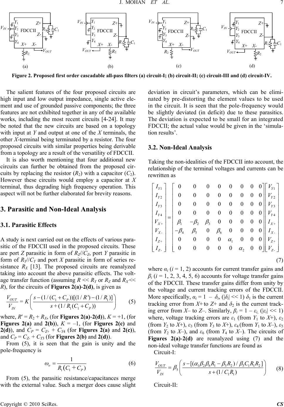 J. MOHAN ET AL. 7 Copyright © 2010 SciRes. CS V IN Y 1 Y 2 Y 3 Y 4 X + X- Z - Z + FDC CІІ V OUT R 1 R 2 C 1 V IN Y 1 Y 2 Y 3 Y 4 X + X- Z - Z + FDC CІІ V OUT R 1 R 2 C 1 (a) (b) V IN Y 1 Y 2 Y 3 Y 4 X +X- Z - Z + FDC CІІ V OUT R 1 R 2 C 1 V IN Y 1 Y 2 Y 3 Y 4 X + X- Z - Z + FDC CІІ V OUT R 1 R 2 C 1 (c) (d) Figure 2. Proposed first order cascadable all-pass filters (a) circuit-I; (b) circuit-II; (c) circuit-III and (d) circuit-IV. The salient features of the four proposed circuits are high input and low output impedance, single active ele- ment and use of grounded passive components; the three features are not exhibited together in any of the available works, including the most recent circuits [4-24]. It may be noted that the new circuits are based on a topology with input at Y and output at one of the X terminals, the other X-terminal being terminated by a resistor. The four proposed circuits with similar properties being derivable from a topology are a result of the versatility of FDCCII. It is also worth mentioning that four additional new circuits can further be obtained from the proposed cir- cuits by replacing the resistor (R2) with a capacitor (C2). However these circuits would employ a capacitor at X terminal, thus degrading high frequency operation. This aspect will not be further elaborated for brevity reasons. 3. Parasitic and Non-Ideal Analysis 3.1. Parasitic Effects A study is next carried out on the effects of various para- sitic of the FDCCII used in the proposed circuits. These are port Z parasitic in form of RZ//CZ, port Y parasitic in form of RY//CY and port X parasitic in form of series re- sistance RX [13]. The proposed circuits are reanalyzed taking into account the above parasitic effects. The volt- age transfer function (assuming R << RY or RZ and RX << R), for the circuits of Figures 2(a)-2(d), is given as 11 11 (1/ ())[(1/')(1/)] =+(1/ ()) OUT P IN P VsCCR R K VsRCC (5) where, R′ = R2 + RX, (for Figures 2(a)-2(d)), K = +1, (for Figures 2(a) and 2(b)), K = –1, (for Figures 2(c) and 2(d)), and CP = CZ+ + CY4 (for Figures 2(a) and 2(c)), and CP = CZ- + CY3 (for Figures 2(b) and 2(d)). From (5), it is seen that the gain is unity and the pole-frequency is 11 1 ) (+ o P ωRCC (6) From (5), the parasitic resistance/capacitances merge with the external value. Such a merger does cause slight deviation in circuit’s parameters, which can be elimi- nated by pre-distorting the element values to be used in the circuit. It is seen that the pole-frequency would be slightly deviated (in deficit) due to these parasitics. The deviation is expected to be small for an integrated FDCCII; the actual value would be given in the ‘simula- tion results’. 3.2. Non-Ideal Analysis Taking the non-idealities of the FDCCII into account, the relationship of the terminal voltages and currents can be rewritten as 11 22 33 44 123 45 6 1 2 00000000 00000000 00000000 00000000 00000 00000 0000 000 0000000 YY YY YY YY X+ X+ X- X- Z +Z+ Z -Z- IV IV IV IV VI VI IV IV (7) where αi (i = 1, 2) accounts for current transfer gains and βi (i = 1, 2, 3, 4, 5, 6) accounts for voltage transfer gains of the FDCCII. These transfer gains differ from unity by the voltage and current tracking errors of the FDCCII. More specifically, αi = 1 – δi, (|δi| << 1) δ1 is the current tracking error from X+ to Z+ and δ2 is the current track- ing error from X– to Z–. Similarly, βi = 1 – εi, (|εi| << 1) where, voltage tracking errors are ε1 (from Y1 to X+), ε2 (from Y2 to X+), ε3 (from Y3 to X+), ε4 (from Y1 to X–), ε5 (from Y2 to X–), and ε6 (from Y4 to X–). The circuits of Figures 2(a)-2(d) are reanalyzed using (7) and the non-ideal voltage transfer functions are found as Circuit-I: 1261 525112 5 11 [() /] (1 /) OUT IN Vs RRCRR VsCR (8) Circuit-II: 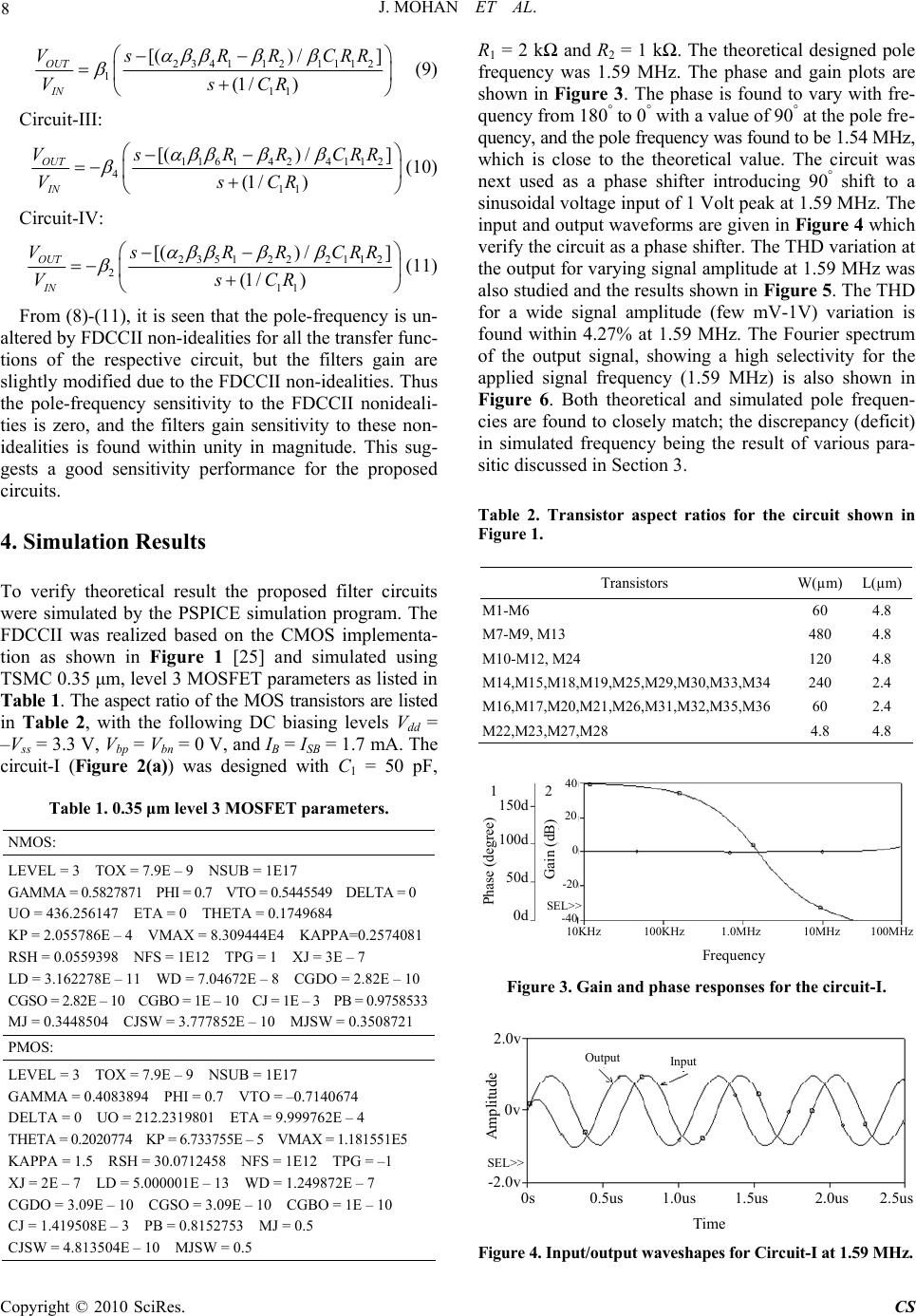 J. MOHAN ET AL. Copyright © 2010 SciRes. CS 8 2341121112 1 11 [() /] (1 /) OUT IN Vs RRCRR VsCR (9) Circuit-III: 11614 24112 4 11 [() /] (1 /) OUT IN VsRRCRR VsCR (10) Circuit-IV: 2351 222112 2 11 [() /] (1 /) OUT IN VsRRCRR VsCR (11) From (8)-(11), it is seen that the pole-frequency is un- altered by FDCCII non-idealities for all the transfer func- tions of the respective circuit, but the filters gain are slightly modified due to the FDCCII non-idealities. Thus the pole-frequency sensitivity to the FDCCII nonideali- ties is zero, and the filters gain sensitivity to these non- idealities is found within unity in magnitude. This sug- gests a good sensitivity performance for the proposed circuits. 4. Simulation Results To verify theoretical result the proposed filter circuits were simulated by the PSPICE simulation program. The FDCCII was realized based on the CMOS implementa- tion as shown in Figure 1 [25] and simulated using TSMC 0.35 μm, level 3 MOSFET parameters as listed in Table 1. The aspect ratio of the MOS transistors are listed in Table 2, with the following DC biasing levels Vdd = –Vss = 3.3 V, Vbp = Vbn = 0 V, and IB = ISB = 1.7 mA. The circuit-I (Figure 2(a)) was designed with C1 = 50 pF, Table 1. 0.35 μm level 3 MOSFET parameters. NMOS: LEVEL = 3 TOX = 7.9E – 9 NSUB = 1E17 GAMMA = 0.5827871 PHI = 0.7 VTO = 0.5445549 DELTA = 0 UO = 436.256147 ETA = 0 THETA = 0.1749684 KP = 2.055786E – 4 VMAX = 8.309444E4 KAPPA=0.2574081 RSH = 0.0559398 NFS = 1E12 TPG = 1 XJ = 3E – 7 LD = 3.162278E – 11 WD = 7.04672E – 8 CGDO = 2.82E – 10 CGSO = 2.82E – 10 CGBO = 1E – 10 CJ = 1E – 3 PB = 0.9758533 MJ = 0.3448504 CJSW = 3.777852E – 10 MJSW = 0.3508721 PMOS: LEVEL = 3 TOX = 7.9E – 9 NSUB = 1E17 GAMMA = 0.4083894 PHI = 0.7 VTO = –0.7140674 DELTA = 0 UO = 212.2319801 ETA = 9.999762E – 4 THETA = 0.2020774 KP = 6.733755E – 5 VMAX = 1.181551E5 KAPPA = 1.5 RSH = 30.0712458 NFS = 1E12 TPG = –1 XJ = 2E – 7 LD = 5.000001E – 13 WD = 1.249872E – 7 CGDO = 3.09E – 10 CGSO = 3.09E – 10 CGBO = 1E – 10 CJ = 1.419508E – 3 PB = 0.8152753 MJ = 0.5 CJSW = 4.813504E – 10 MJSW = 0.5 R1 = 2 kΩ and R2 = 1 kΩ. The theoretical designed pole frequency was 1.59 MHz. The phase and gain plots are shown in Figure 3. The phase is found to vary with fre- quency from 180° to 0° with a value of 90° at the pole fre- quency, and the pole frequency was found to be 1.54 MHz, which is close to the theoretical value. The circuit was next used as a phase shifter introducing 90° shift to a sinusoidal voltage input of 1 Volt peak at 1.59 MHz. The input and output waveforms are given in Figure 4 which verify the circuit as a phase shifter. The THD variation at the output for varying signal amplitude at 1.59 MHz was also studied and the results shown in Figure 5. The THD for a wide signal amplitude (few mV-1V) variation is found within 4.27% at 1.59 MHz. The Fourier spectrum of the output signal, showing a high selectivity for the applied signal frequency (1.59 MHz) is also shown in Figure 6. Both theoretical and simulated pole frequen- cies are found to closely match; the discrepancy (deficit) in simulated frequency being the result of various para- sitic discussed in Section 3. Table 2. Transistor aspect ratios for the circuit shown in Figure 1. Transistors W(µm)L(µm) M1-M6 60 4.8 M7-M9, M13 480 4.8 M10-M12, M24 120 4.8 M14,M15,M18,M19,M25,M29,M30,M33,M34 240 2.4 M16,M17,M20,M21,M26,M31,M32,M35,M36 60 2.4 M22,M23,M27,M28 4.8 4.8 1 Phase (degree) 150d 100d 50d 0d Frequency 10KHz 100KHz 1.0MHz 10MHz 100MHz Gain (dB) 2 40 20 0 -20 -40 SEL>> Figure 3. Gain and phase responses for the circuit-I. Time 0s 0.5us 1.0us 1.5us 2.0us 2.5us Amplitude Output 2.0v 0v -2.0v SEL >> Input Figure 4. Input/output waveshapes for Circuit-I at 1.59 MHz.  J. MOHAN ET AL. Copyright © 2010 SciRes. CS 9 VIN (mV) 0.1 1 10 100 1000 THD (%) 6 4 2 0 Figure 5. THD variation at output with signal amplitude at 1.59 MHz. Frequency 0Hz 4MHz 8MHz 12MHz 1.0 v 0 v 0.5v SEL>> V ( 1 ) V ( 4 ) Figure 6. Fourier spectrum of Input-output signal at 1.59 MHz. Similarly, the circuit-III (Figure 2(c)) was designed with the same values and frequency as above. The phase and gain plots are shown in Figure 7. The phase is found to vary with frequency from 0 to –180° with a value of –90° at the pole frequency, and the pole frequency was found to be 1.54 MHz, which is close to the theoretical value. The circuit was next used as a phase shifter intro- ducing –90° shift to a sinusoidal voltage input of 1 Volt peak at 1.59 MHz. The input and output waveforms are given in Figure 8 which verify the circuit as a phase shifter. 5. Application Example To further illustrate the utility of the proposed circuits a sinusoidal oscillator producing a number of quadrature signals was realized using the Circuit-I (Figure 2(a)). By connecting Y2 terminal, the input node to the Z-terminal of FDCCII, connecting resistor (R′) and capacitor (C′) at X– and Z– terminals of FDCCII. The resulting circuit is shown in Figure 9. The circuit analysis yields the fol- lowing characteristic equation 1 Phase (degree) 0d -50d -100d -180d Frequency 10KHz 100KHz 1.0MHz 10MHz 100MHz Gain (dB) 2 40 20 0 -20 -40 SEL>> Figure 7. Gain and phase responses for the circuit-III. Time 0.5us 1.0us 1.5us 2.0us 2.5us 3.0us Amplitude Output 2.0v 0 v -2.0v SE L>> Input Figure 8. Input/output waveshapes for Circuit-III at 1.59 MHz. V OUT1 R 1 R 2 C 1 V OUT2 R ’ V OUT3 C ’ Y 1 Y 2 Y 3 Y 4 Z + Z - X + X - FDC C ІІ Figure 9. Multiphase oscillator using Circuit-I of Figure 2(a). 212 111 12 11 0 ''' ' RR ss CRC RCC RRR (12) At the frequency of oscillation, with s = jω, the Equa- tion (5) gives the frequency of oscillation (FO) and con- dition of oscillation (CO) as 12 112 :'' O RR FO ωCCRR R; CO: C′R′ ≥ C1R1 (13) Assuming R′ = R1 = 2R2; C′ = C1  J. MOHAN ET AL. Copyright © 2010 SciRes. CS 10 1 :2'' O FO ωCR (14) From Figure 9, at oscillating frequency the circuit pro- vides three quadrature voltage outputs (VOUT1, VOUT2 and VOUT3) whose phasor relationship is shown in Figure 10. The circuit was designed with C1 = C′ = 50 pF, R1 = R′ = 2 kΩ, and R2 = 1 kΩ, the theoretical frequency of os- cillation was around fo = 1.59 MHz, whereas the simu- lated values as found from the result was fo = 1.54 MHz. The quadrature oscillations are shown in Figure 11. 6. Conclusions This paper has presented four new first-order VM casca- dable all-pass sections, each employing single FDCCII, two resistors and one capacitor. The salient features of all the proposed circuits are high input and low output im- pedance, single active element and use of grounded pa- ssive components. The proposed circuits with grounded components in each case are suited for IC implementa- tion in CMOS technology. Non-ideality aspects and par- asitic effects are also studied. The circuits are verified th- rough PSPICE simulations using TSMC 0.35 µm CMOS parameters. Application example in the form of multi- phase oscillator is also given and also verified with good results. The proposed circuits are ideal for voltage-mode applications as well as good for IC implementation, mak- ing them a future prospect for integration. VOUT1 VOUT2 VOUT3 Figure 10. Phasor diagram of multiphase oscillator. Time 0s 0.5us 1.0us 1.5us 2.0us 2.5us Amplitude V OUT1 1.0v 0v SEL>> V OUT2 V OUT3 -1.0v Figure 11. Quadrature voltage outputs of multiphase oscil- lator. 7. Acknowledgements The authors would like to thank the anonymous review- ers for their valuable comments. 8. References [1] M. Bhusan and R. W. Newcomb, “Grounding of Capaci- tors in Integrated Circuits,” Electronics Letters, Vol. 3, No. 4, 1967, pp. 148-149. [2] D. Biolek, R. Senani, V. Biolkova and Z. Kolka, “Active Elements for Analog Signal Processing: Classification, Review, and New Proposals,” Radioengineering, Vol. 17, No. 4, 2008, pp. 15-32. [3] S. J. G. Gift, “The Application of All-Pass Filters in the Design of Multiphase Sinusoidal Systems,” Microelec- tronics Journal, Vol. 31, No. 1, 2000, pp. 9-13. [4] A. M. Soliman, “Inductorless Realization of an All-Pass Transfer Function Using the Current Conveyor,” IEEE Transactions on Circuits Theory, Vol. 20, 1973, pp. 80-81. [5] A. M. Soliman, “Generation of Current Conveyor-Based All-Pass Filters from Op Amp-Based Circuits,” IEEE Transactions on Circuits and Systems II: Analog and Digital Signal Processing, Vol. 44, No. 4, 1997, pp. 324-330. [6] M. Higashimura and Y. Fukui, “Realization of All-Pass Network Using a Current Conveyor,” International Jour- nal of Electronics, Vol. 65, No. 22, 1988, pp. 249-250. [7] O. Cicekoglu, H. Kuntman and S. Berk, “All-Pass Filters Using a Single Current Conveyor,” International Journal of Electronics, Vol. 86, No. 8, 1999, pp. 947-955. [8] I. A. Khan and S. Maheshwari, “Simple First Order All- Pass Section Using a Single CCII,” International Journal of Electronics, Vol. 87, No. 3, 2000, pp. 303-306. [9] A. Toker, S. Özcan, H. Kuntman and O. Çiçekoglu, “Su- pplementary All-Pass Sections with Reduced Number of Passive Elements Using a Single Current Conveyor,” In- ternational Journal of Electronics, Vol. 88, No. 9, 2001, pp. 969-976. [10] M. A. Ibrahim, H. Kuntman and O. Cicekoglu, “First- Order All-Pass Filter Canonical in the Number of Resis- tors and Capacitors Employing a Single DDCC,” Circuits, Systems, and Signal Processing, Vol. 22, No. 5, 2003, pp. 525-536. [11] N. Pandey and S. K. Paul, “All-Pass Filters Based on CCII- and CCCII-,” International Journal of Electronics, Vol. 91, No. 8, 2004, pp. 485-489. [12] K. Pal and S. Rana, “Some New First-Order All-Pass Realizations Using CCII,” Active and Passive Electronic Component, Vol. 27, No. 2, 2004, pp. 91-94. [13] S. Maheshwari, I. A. Khan and J. Mohan, “Grounded Capacitor First-Order Filters Including Canonical Forms,” Journal of Circuits, Systems and Computers, Vol. 15, No. 2, 2006, pp. 289-300. [14] J. W. Horng, C. L. Hou, C. M. Chang, Y. T. Lin, I. C.  J. MOHAN ET AL. Copyright © 2010 SciRes. CS 11 Shiu and W. Y. Chiu, “First-Order All-Pass Filter and Sinusoidal Oscillators Using DDCCs,” International Jour- nal of Electronics, Vol. 93, No. 7, 2006, pp. 457-466. [15] S. Minaei and O. Cicekoglu, “A Resistorless Realization of the First Order All-Pass Filter,” International Journal of Electronics, Vol. 93, No. 3, 2006, pp. 177-183. [16] H. P. Chen and K. H. Wu, “Grounded Capacitor First Order Filter Using Minimum Components,” IEICE Trans- actions on Fundamentals of Electronics Communications and Computer Science, Vol. E89-A, No. 12, 2006, pp. 3730-3731. [17] S. Maheshwari, “High Input Impedence VM-APSs with Grounded Passive Elements,” IET Circuits Devices and Systems, Vol. 1, No. 1, 2007, pp. 72-78. [18] S. Maheshwari, “High Input Impedance Voltage Mode First Order All-Pass Sections,” International Journal of Circuit Theory and Application, Vol. 36, No. 4, 2008, pp. 511-522. [19] S. Maheshwari, “Analog Signal Processing Applications Using a New Circuit Topology,” IET Circuits Devices Systems, Vol. 3, No. 3, 2009, pp. 106-115. [20] B. Metin and O. Cicekoglu, “Component Reduced All- Pass Filter with a Grounded Capacitor and High Imped- ance Input,” International Journal of Electronics, Vol. 96, No. 5, 2009, pp. 445-455. [21] D. Biolek and V. Biolkova, “Allpass Filter Employing one Grounded Capacitor and one Active Element,” Elec- tronics Letters, Vol. 45, No. 16, 2009, pp. 807-808. [22] D. Biolek and V. Biolkova, “First Order Voltage-Mode All-Pass Filter Employing One Active Element and One Grounded Capacitor,” Analog Integrated Circuit and Sig- nal Processing, Vol. 45, No. 16, 2009, pp. 807-808. [23] T. Tsukutani, H. Tsunetsugu, Y. Sumi and N. Yabuki, “Electronically Tunable First-Order All-Pass Circuit Em- ploying DVCC and OTA,” International Journal of Elec- tronics, Vol. 97, No. 3, 2010, pp. 285-293. [24] S. Minaei and E. Yuce, “Novel Voltage-Mode All-Pass Filter Based on Using DVCCs,” Circuits, Systems, and Signal Processing, Vol. 29, No. 3, 2010, pp. 391-402. [25] A. A. El-Adway, A. M. Soliman and H. O. Elwan, “A Novel Fully Differential Current Conveyor and its Ap- plication for Analog VLSI,” IEEE Transactions on Cir- cuits and Systems II: Analog and Digital Signal Process- ing, Vol. 47, No. 4, 2000, pp. 306-313. [26] C. M. Chang, B. M. Al-Hashimi, C. I. Wang and C. W. Hung, “Single Fully Differential Current Conveyor Bi- quad Filters,” IEE Proceedings on Circuits, Devices and Systems, Vol. 150, No. 5, 2003, pp. 394-398. [27] J. W. Horng, C. L. Hou, C. M. Chang, H. P. Chou, C. T. Lin and Y. Wen, “Quadrature Oscillators with Grounded Capacitors and Resistors Using FDCCIIs,” ETRI Journal., Vol. 28, No. 4, 2006, pp. 486-494. |