Journal of Minerals and Materials Characterization and Engineering, 2012, 11, 724-729
Published Online July 2012 (http://www.SciRP.org/journal/jmmce)
Influence of Sputter Deposition Time on the Growth
of c-Axis Oriented AlN/Si Thin Films for
Microelectronic Application
V. VasanthiPillay1, K. Vijayalakshmi2*
1Department of Physics, Sujatha Degree and PG College for Women, Hyderabad, India
2Department of Physics, Bishop Heber College, Tiruchirappalli, India
Email: v.vasanthipillayphy@gmail.com, *viji71naveen@yahoo.com
Received April 27, 2012; revised June 7, 2012; accepted June 30, 2012
ABSTRACT
Aluminum Nitride films were grown on and Si (100) substrate by DC reactive magnetron sputtering at room tempera-
ture. Influence of sputter deposition time on properties of the AlN films was studied. Structural optical and electrical
properties of the film were investigated. XRD measurements showed the presence of hexagonal wurtzite structure. The
optical reflectance spectra of the film were taken and the band gap calculated varied from 4.35 to 5.3 eV. Finally MIS
capacitors were fabricated on silicon substrates and variation of dielectric parameter with deposition time was reported.
Keywords: Aluminum Nitride; Thin Films; Sputtering; Preferential Orientations
1. Introduction
Aluminum Nitride (AlN) and its alloys are the most at-
tractive material investigated over the past several years
[1-3]. Growth of high-quality epitaxial wurtzite ALN
thin film on different substrates have been of great inter-
est due to their peculiar features such as high electrical
resistivity (1011 - 1013 ohm·cm), high thermal conductiv-
ity, high hardness (11 - 15 GPa), wideband gap 6.0 - 6.2
eV and high velocity of acoustic waves etc. The combi-
nation of these characteristics makes AlN thin films a
promising material for many electronic, optoelectronic,
acoustic devices such as surface acoustic wave (SAW)
[4,5]. The characteristics of AlN films are greatly influ-
enced by their microstructure. Growth of smooth surface
and defect less structure were the goal of device devel-
opment. Various deposition techniques and substrates
have been employed in an attempt of achieving high
quality growth; the most frequently used substrates are
Al2O3, SiC, Si (111) and Si (100). The later is of special
interest because of the possibility to integrate with the
contemporary Si device technology for different func-
tions, e.g. UV detection or emission and Si-ICs on a
common substrate.
In the past years several methods have been developed
to prepare AlN thin films, such as chemical vapor depo-
sition (CVD), molecular beam epitaxy (MBE), pulsed
laser deposition (PLD), ion-beam assisted deposition and
reactive sputtering [6-9]. However, these methods are
expensive and the required high temperatures to reach
satisfying properties are often incompatible with micro-
electronic processes. Among other techniques, the reac-
tive magnetron sputtering process (RMS) is an attractive
deposition technique because it presents advantages of
being low temperature and low cost methods, and it al-
lows fine-tuning of the material characteristics [10-12].
2. Experimental
AlN films were deposited with a 99.5% pure Al target
DC magnetron sputtering system operated at 60 W DC
cathode power and in pure Ar and N2 gas mixture, which
was introduced into the chamber by separate mass flow
controllers. The deposition of ALN films can take place
in a wide range of temperatures from room temperature
up to 400˚C. High temperature deposition has the disad-
vantage of producing degradation of the substrate, in-
corporation of impurities and thermal damage to the
growing film. Hence deposition of AlN films at low
temperature has become increasingly important and
value [13]. Therefore AlN films were grown on (100)
oriented silicon substrate at room temperature. Degreas-
ing of glass was carried out ultrasonically in successive
baths of acetone, ethanol and deionized water, and the
native oxide on the silicon wafer was removed through
an etching step in dilute HF solution. After this initial
cleaning process, high purity Ar gas was introduced into
*Corresponding author.
Copyright © 2012 SciRes. JMMCE
V. VASANTHIPILLAY, K. VIJAYALAKSHMI 725
the chamber and the chamber was evacuated to below 1 ×
105 mbar. Then prior to each run the target was pre-
sputtered with argon gas for 5 minutes with the target
shutter closed. During pre sputtering DC power and Ar
pressure was kept constant at 60 W and 1 × 10⁵ mbar
respectively, then nitrogen was introduced into chamber
and reactive sputtering was initiated. AlN films were
grown on Si substrate for different deposition time keep-
ing the other deposition parameters constant. A summary
of deposition parameters and ranges used in AlN thin
films is listed in Table 1. For electrical measurements,
Metal-insulator-semiconductor (MIS) structures were
formed by sputter deposition through a metal mask of Al
dots on AlN film as top electrode and a continuous Al
film on Si wafer backside as bottom electrode.
The thickness of the films measured using stylus pro-
filometer for 2, 4, 6, 8 minutes of deposition time were
49, 81, 102, 114 nm respectively. The type of crystalline
structure, orientation and grain size was examined by
X-ray diffraction (XRD). Optical studies were carried out
by UV-visible spectrometer and band gap was calculated
from the obtained reflectance spectra. Finally dielectric
parameters were measured using impedance analyzer in
frequency range 1 KHz to 1 MHz at room temperature.
3. Results and Discussion
3.1. XRD Analysis
AlN films were deposited on Si (100) substrate for dif-
ferent deposition time, keeping the sputtering pressure,
Table 1. AlN deposition parameters.
Parameters Values
Deposition process DC magnetron sputtering
Magnetron Disc
Area of cathode (target), inch 2
Material of the target Al
Discharge voltage, V 510
Discharge current, mA 117
Substrate Silicon (100)
Substrate temperature in Kelvin 300
Working gases Ar + N2
Initial pressure in chamber, mbar 1.3 × 10⁴
Partial pressure of active (N2), mbar5 × 105
Total pressure in the chamber, mbar1 × 103
Distance between the cathode and
anode, cm 4
Deposition time, minutes 2, 4, 6, 8
target power, substrate target distance and nitrogen con-
centration constant. XRD analysis were carried out using
RIGAKU X-ray diffractometer employing Cu Kα (1.5406
Å) radiation; θ - 2θ scans were performed with step size
of 0.05 at a scan speed of 3 sec per step in the range of
10 - 80. The diffraction planes in θ - 2θ method are par-
allel to the sample surface. Accordingly, this method is
very helpful in studying preferred orientation in thin film
materials when compared to grazing angle incidence me-
thod [15]. The influence of deposition time on the crys-
talline orientation of AlN films has been investigated. All
the deposited films were found to have hexagonal wurtz-
ite structure. Figure 1 shows the XRD pattern of AlN
films on Si substrate for different deposition time. The
micro structural properties and the lattice disorders are
studied from the analysis of XRD peaks, and are listed in
Table 2. The mean crystallite size was found to be ~60
nm. By substituting the measured crystallite size, the
strain in the films can be determined using the following
equation ε = (β/tanθ) – (kλ/sinθ). In addition, it is evident
that, both strain and dislocation density increases with
increase in deposition time, which reveals the increase of
particle collision due to the augmentation of stress in the
lattice.
The crystal orientation of AlN films was strongly de-
pendent on deposition conditions. It was found that under
low deposition time of 2 min the film presents features at
32.98˚ and 36˚ corresponding to (100). As the deposition
time increased to 4 min and 6 min, the intensity of AlN
(100) plane is decreased, while the intensity of AlN (002)
Figure 1. X-ray intensity vs. the diffraction angle 2θ of AlN
thin films deposited on Si (100) substrate at different depo-
ition time: (a) 2 m; (b) 4 m; (c) 6 m; (d) 8 m. s
Copyright © 2012 SciRes. JMMCE
V. VASANTHIPILLAY, K. VIJAYALAKSHMI
JMMCE
726
Table 2. Structural parameters calculated from XRD data.
Time min d spacing (dhkl) Å Crystallite size (D) nmStrain (ε) Dislocation density (δ) lines/m2
2 2.7137 61.40 4.48 × 10⁴ 2.8492
4 2.7105 61.40 4.82 × 10⁴ 2.9491
6 2.7121 57.47 5.47 × 10⁴ 3.3807
8 2.7121 57.47 5.78 × 10⁴ 3.8147
plane is enhanced. Further increasing the deposition time
to 8 min resulted in films with highly oriented (002)
(JCPDS file No. 00-0025-1133), with less intense AlN
(100) plane.
The mechanism of preferential orientation of AlN film
can be explained by the crystalline lattice structure of
AlN. The hexagonal wurtzite structure of AlN has two
kinds of AlN bonds named B1 and B2 [16]. The forma-
tion energy of the B2 bond is larger than that of B1. {100}
plane consists of only B1 bonds, while {002} and {101}
consist of B1 and B2 bonds together. Accordingly ad at-
oms with more energy favor the formation of {002} sur-
face plane. Another factor, which strongly influences the
formation of preferred surface planes, is packing habit of
such planes. For the development of close-packed sur-
face planes the ad atoms need a longer time to accom-
modate themselves into the low energy configured lattice
sites before the arrival of the next layer of reactive spe-
cies. A low deposition rate is necessary in such cases
[13]. Hence, we predict that at a deposition time of 8 min,
the coated film has low deposition rate, which favors the
formation of highly oriented (002) preferential plane with
enhanced crystal quality, which can provide good piezo-
electric response.
Figure 2. Reflectance spectra of AlN thin film on Si (100) at
different deposition time: (a) 2 m; (b) 4 m; (c) 6 m; (d) 8 m
the films.
3.2. Optical Properties
The optical reflectance of the films has been recorded
employing a Perkin-Elmer Lamba-950 spectrometer. The
optical energy band gap of AlN films is determined by
analyzing the optical data with the expression for the
reflectance and photon energy using the Tauc relation

n2
g
AhE
2h

(1)
where n is the constant, which is equal to one for direct
band gap semi-conducting material and four for and in-
direct band gap semi-conducting material. hν is the pho-
ton energy, and α the absorption coefficient, which can
be written in terms of reflectance as 2αt = ln[(Rmax
Rmin)/(R Rmin)] where t is the thickness of the sample
and R the reflectance for any intermediate photon energy.
Figure 2 shows the reflectance spectra of AlN thin film
on Si substrate for different deposition time. A fall in
reflectance is observed from Rmax to Rmin due to absorp-
tion of light by the material. Figure 3 shows, a graph is
Figure 3. Graph between (αhν)2 and hν.
plotted between (αhν)2 and hν using Equation (1). The
extrapolation of linear portion of the plot of the energy
axis (αhν)2 = 0 gives the value of the energy band gap of
the thin film. It is found that the energy band gap of the
AlN film varies from 4.35 to 5.3 eV. It is clear that the
energy band gap of AlN films increases with increase in
the deposition time. This variation in band gap is attrib-
uted to the internal strain in the films which increases
Copyright © 2012 SciRes.
V. VASANTHIPILLAY, K. VIJAYALAKSHMI 727
with the deposition time as shown in the Table 2. The
refractive index (η) of the sputter-deposited AlN is de-
pendent on the sputtering conditions since it is related to
the composition and density of the films.
For polycrystalline AlN films obtained by DC reactive
sputtering, the refractive index varies from 1.9 to 2.1.
The refractive index of our AlN samples, determined
from the dielectric measurement of ε and δ, revealed that
they are in the range of 1.1 - 1.2, for the AlN samples
prepared at a deposition time of 8 minutes. The decrease
in the refractive index values is observed in the presence
of impurities (such as oxygen) or nitrogen vacancies
present in the film [17].
3.3. Electrical Properties
The variation of the dielectric parameters, such as C, ε
and tanδ of MIS capacitors with deposition time was
studied in the frequency range from 10 KHz - 1 MHz
using impedance analyzer at room temperature. Plots of
the dielectric constant ε, loss factor tan δ and capacitance
C as a functions of the frequency for different deposition
time of AlN films are shown in Figures 4(a)-(c). The
capacitance of the thin insulating film almost remains
constant in the frequency range from 10 KHz - 1 MHz,
with its value varying from 0.8 × 10⁸ to 1.8 × 10⁷ µF. It
is observed that, as the deposition time increases the ca-
pacitance decreases with least value at 8 minutes of
deposition time.
The dielectric constant of AlN films was between 6.0
and 6.8, which is similar with reported values for AlN
[15]. The real part of dielectric constant increases with
increasing deposition time and decreases with increasing
frequency. The observed dependence of the dielectric
constant on the dielectric film thickness (deposition time)
for thinner films (less than ~1000) is attributed to defects
such as voids, stresses, in homogeneity, grain boundaries,
discontinuities etc, which are normally present in vac-
uum-deposited films, rather than to the non-stoichiome-
try of the deposits resulting from an excess of oxygen or
metal atoms. Some of these defects are removed by self-
annealing or aging processes, but others require more
thermal energy such as is provided by an annealing pro-
cess. As the films become thicker, the density of voids
decreases, resulting in a higher value of dielectric con-
stant, which evidently becomes thickness independent.
Adam et al. [17] reported the dependence of dielectric
constant on film thickness. The dielectric constant was
between 4 and 11 for thicker layers (100 Å) and de-
creased to values between 2 and 6 for thicknesses below
100 Å. And Dimitrova et al. [18] reported low dielectric
constants (6.8 - 7.1) due to the presence of nitrogen va-
cancies in the AlN lattice.
The dielectric dissipation factor tanδ of an insulating
(a)
(b)
(c)
Figure 4. (a) Graph betw een capacitance and frequency for
different deposition time; (b) Graph between dielectric con-
stant and frequency for different deposition time; (c) Graph
between dissipation factor and frequency for different depo-
sition time.
Copyright © 2012 SciRes. JMMCE
V. VASANTHIPILLAY, K. VIJAYALAKSHMI
728
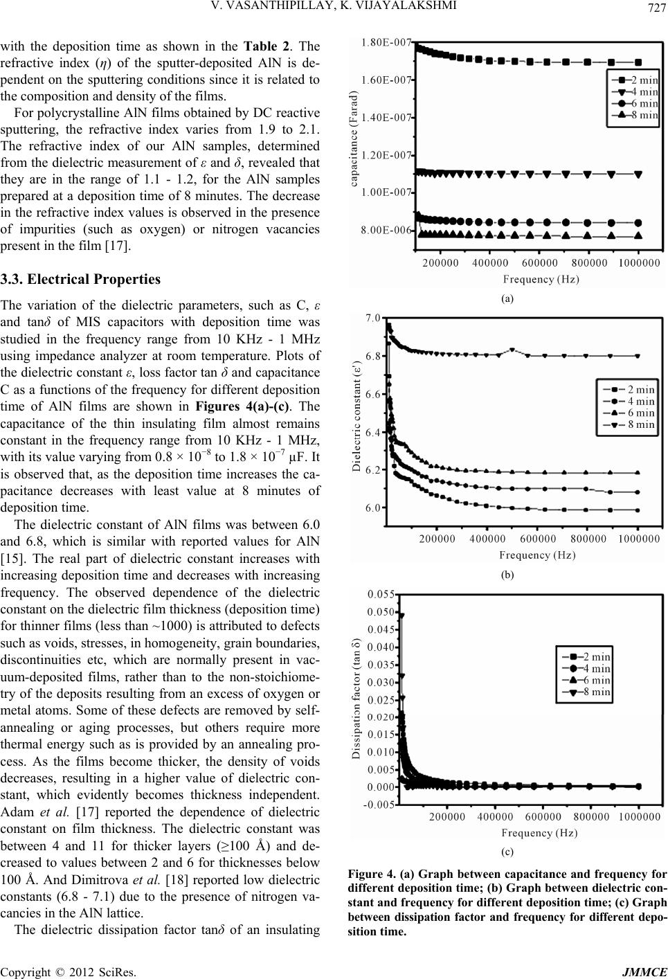
material is the tangent of the loss angle δ. In a perfect
dielectric, the voltage wave and the current are exactly 90˚
out of phase. As the dielectric becomes less than 100%
efficient, the current wave begins to lag the voltage in
direct proportion. The amount the current wave deviates
from being 90˚ out of phase with the voltage is defined as
the dielectric loss angle. The tangent of this angle is
known as the loss tangent or dissipation factor [19].
Hence a good dielectric film should have minimum dis-
sipation factor. In the present study, the dissipation factor
varies from 0.0011 to 0.004 and is independent of the
deposition time. It almost remains constant for all the
films with different deposition time.
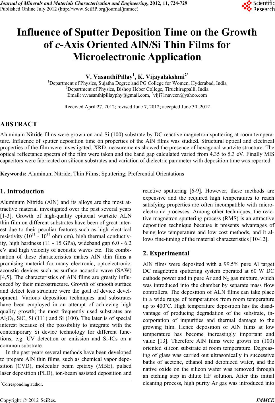
4. Conclusion
AlN films have been prepared by DC reactive magnetron
sputtering on Si (100) substrates for different deposition
time. The evolution of preferred orientation and mor-
phology of AlN films deposited at 50% nitrogen concen-
tration on Si (100) substrate was studied. The XRD
analysis of the films revealed that, at a deposition time of
8 min, the coated film favored the formation of highly
oriented (002) preferential plane with enhanced crystal
quality, which can provide good piezoelectric response.
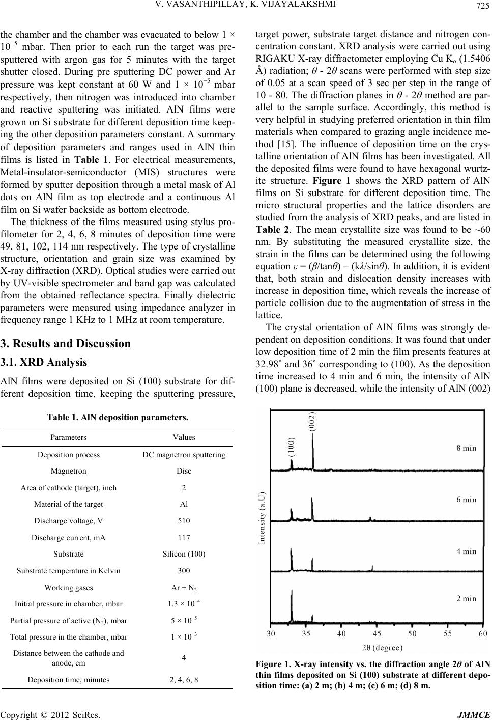
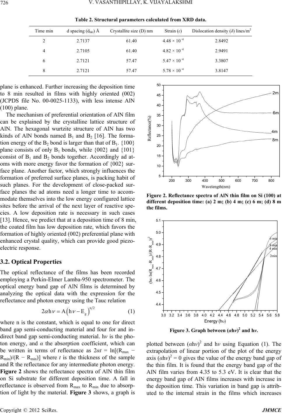
The optical reflectance spectra show reflectance at 240
nm. The band gap increased with the increase in the
deposition time and the values of refractive index were in
the range of 1.1 - 1.2, for the samples prepared at 8 min
of deposition time. The MIS structures fabricated using
AlN at different deposition time showed a significant
improvement of electrical characteristics with deposition
time as we go from 2 min to 8 min.
REFERENCES
[1] B. Mednikarov, G. Spasov and T. Babeva, “Aluminum
Nitride Layer Prepared by DC/RF Magnetron Sputter-
ing,” Journal of Optoelectronics and Advanced Materials,
Vol. 7, No. 3, 2005, pp. 1421-1427
[2] T. P. Drusedau and J. Blasing, “Optical and Structural
Properties of Highly c-Axis Oriented Aluminum Nitride
Prepared by Sputter-Deposition in Pure Nitrogen,” Thin
Solid Films, Vol. 377-378, 2000, pp. 27-31.
doi:10.1016/S0040-6090(00)01380-8
[3] X. H. Ji, S. P. Lau, G. Q. Yu, W. H. Zhong and B. K. Tay,
“Structural Properties and Nanoindentation of AlN Films
by a Filtered Cathodic Vacuum Arc at Low Tempera-
ture,” Journal of Physics D: Applied Physics, Vol. 37,
No. 10, 2004, p. 1472. doi:10.1088/0022-3727/37/10/009
[4] M. Clement, L. Vergara, J. Sangardor, E. Iborra and A.
Sanz-Herras, “SAW Characteristics of AlN Films Sput-
tered on Silicon Substrates,” Ultrasonic, Vol. 42, No. 1-9,
2004, pp. 403-407. doi:10.1016/j.ultras.2004.01.034
[5] T. Palacios, F. Calle, E. Monroy, J. Grajal, M. Eickhoff,
O. Ambacher and C. Prieto, “Nanotechnology for SAW
Devices on AlN Epilayers,” Materials Science and Engi-
neering: B, Vol. 93, No. 1-3, 2000, pp. 154-158.
doi:10.1016/S0921-5107(02)00022-3
[6] H. Gong and X. Jiang, “c-Axis Oriented AlN Films Pre-
pared on Diamond Film Substrate by Electron Cyclotron
Resonance Plasma Enhanced Chemical Vapour Deposi-
ton,” Journal of Crystal Growth, Vol. 235, No. 1-4, 2000,
pp. 333-339.
[7] A. J. Shuskus, T. M. Reeder and E. L. Paradis, “RF-Sput-
tered Aluminum Nitride Films on Sapphire,” Applied Phys-
ics Letters, Vol. 24, No. 4, 1974, pp. 155-156.
doi:10.1063/1.1655132
[8] M. Ishihara, K. Yamamoto, F. Kokai and Y. Koga, “Aluimi-
num Nitride Thin Films Prepared by Radical-Assisted
Pulsed Laser Deposition,” Vaccum, Vol. 59, No. 2-3,
2000, pp. 649-656. doi:10.1016/S0042-207X(00)00329-8
[9] L. Huang, X. D. Wang, K. W. Hipps, U. Mazur, R. Hef-
fron and J. T. Dickinson, “Chemical Etching of Ion Beam
Deposited AlN and AlN:H,” Thin Solid Films, Vol. 279,
No. 1-2, 1996, pp. 43-48.
[10] M. M. D. Ramos, J. B. Almeida, M. I. C. Ferrerira and M.
P. D. Santos, “Thin Film Deposition by Magnetron Sput-
tering and Determination of Some Physical Parameters,”
Thin Solid Films, Vol. 176, No. 2, 1989, pp. 219-226.
doi:10.1016/0040-6090(89)90095-3
[11] J. Huang, L. Wang, Q. Shen, C. Lin and O. Milae, “Prepa-
ration of AlN Films by Nitridation of Al Coated Si Sun-
strate,” Thin Solid Films, Vol. 340, No. 1-2, 1999, pp.
137-139. doi:10.1016/S0040-6090(98)01373-X
[12] V. Dimitrova, D. Monova, T. Paskova, Tz. Uzunov, N.
Lvanoc and D. Dechev, “Aluminum Nitride Thin Films
Deposited by DC Reactive Magnetron Sputtering FN2,”
Vaccum, Vol. 51, No. 2, 1998, pp. 161-164.
[13] M. Ishihara, K. Yamamoto, F. Kokai and Y. Koga, “Effect
of Laser Wavelength for Surface Morphology of Alumi-
num Nitride Thin Films by Nitrogen Radical-Assisted
Pulsed Laser Deposition,” Japanese Journal of Applied
Physics, Vol. 40, No. 575, 2001, pp. 2413-2416.
doi:10.1143/JJAP.40.2413
[14] H. Cheng, Y. Sun, J. X. Zhang, S. Yuan and P. Hing,
“AlN Films Deposited under Various Nitrogen Concen-
trations by RF Reactive Sputtering,” Journal of Crystal
Growth, Vol. 254, No. 1-2, 2003, pp. 46-54.
doi:10.1016/S0022-0248(03)01176-X
[15] X. H. Xu, C. J. Zhang and Z. H. Jin, “Morphological
Properties of AlN Piezoelectric Thin Films Deposited by
DC Reactive Magnetron Sputtering,” Thin Solid Films,
Vol. 388, No. 1-2, 2001, pp. 62-67.
doi:10.1016/S0040-6090(00)01914-3
[16] Z. Q. Yao, Y. Q. Li, J. X. Tang, W. J. Zhang and S. T.
Lee, “Growth and Photoluminescence Studies of AlN
Thin Films with Different Orientation Degrees,” Dia-
mond and Related Materials, Vol. 17, No. 7-10, 2008, pp.
1785-1790. doi:10.1016/j.diamond.2008.02.009
[17] T. Adam, J. Kolodzey, C. P. Swann, M. W. Tsao and J. F.
Rabolt, Vol. 175-176, 2001, pp. 428-435.
[18] V. Dimitrova, D. Manova and E. Valcheva, “Optical and
Dielectric Properties of DC Magnetron Sputtered AlN
Copyright © 2012 SciRes. JMMCE
V. VASANTHIPILLAY, K. VIJAYALAKSHMI
Copyright © 2012 SciRes. JMMCE
729
Thin Films Correlated with Deposition Conditions,” Ma-
terials Science and Engineering: B, Vol. 68, No. 1, 1999,
pp. 1-4. doi:10.1016/S0921-5107(99)00221-4
[19] K. Jagannadham, A. K. Sharma, Q. Wei, R. Kalayanra-
man and J. Narayan, “Structural Characteristics of AlN
Films Deposited by Pulsed Laser Deposition and Reactive
Magnetron Sputtering: A Comparative Study,” Journal of
Vac- uum Science & Technology A, Vol. 16, No.5, 1998,
pp. 2804-2816. doi:10.1116/1.581425