Paper Menu >>
Journal Menu >>
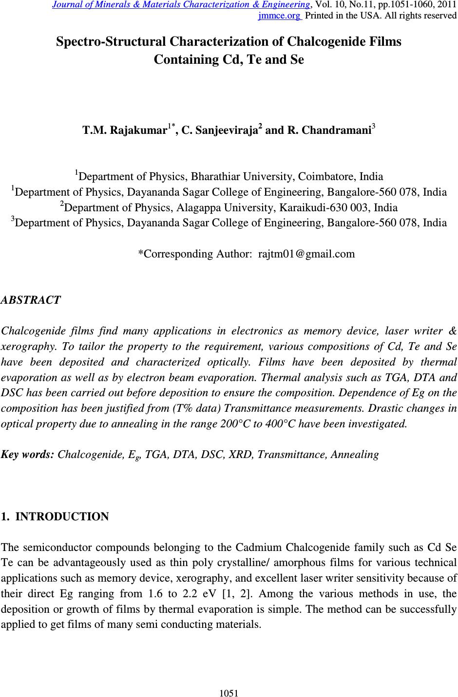 Journal of Minerals & Materials Characterization & Engineering, Vol. 10, No.11, pp.1051-1060, 2011 jmmce.org Printed in the USA. All rights reserved 1051 Spectro-Structural Characterization of Chalcogenide Films Containing Cd, Te and Se T.M. Rajakumar 1* , C. Sanjeeviraja 2 and R. Chandramani 3 1 Department of Physics, Bharathiar University, Coimbatore, India 1 Department of Physics, Dayananda Sagar College of Engineering, Bangalore-560 078, India 2 Department of Physics, Alagappa University, Karaikudi-630 003, India 3 Department of Physics, Dayananda Sagar College of Engineering, Bangalore-560 078, India *Corresponding Author: rajtm01@gmail.com ABSTRACT Chalcogenide films find many applications in electronics as memory device, laser writer & xerography. To tailor the property to the requirement, various compositions of Cd, Te and Se have been deposited and characterized optically. Films have been deposited by thermal evaporation as well as by electron beam evaporation. Thermal analysis such as TGA, DTA and DSC has been carried out before deposition to ensure the composition. Dependence of Eg on the composition has been justified from (T% data) Transmittance measurements. Drastic changes in optical property due to annealing in the range 200°C to 400°C have been investigated. Key words: Chalcogenide, E g , TGA, DTA, DSC, XRD, Transmittance, Annealing 1. INTRODUCTION The semiconductor compounds belonging to the Cadmium Chalcogenide family such as Cd Se Te can be advantageously used as thin poly crystalline/ amorphous films for various technical applications such as memory device, xerography, and excellent laser writer sensitivity because of their direct Eg ranging from 1.6 to 2.2 eV [1, 2]. Among the various methods in use, the deposition or growth of films by thermal evaporation is simple. The method can be successfully applied to get films of many semi conducting materials. 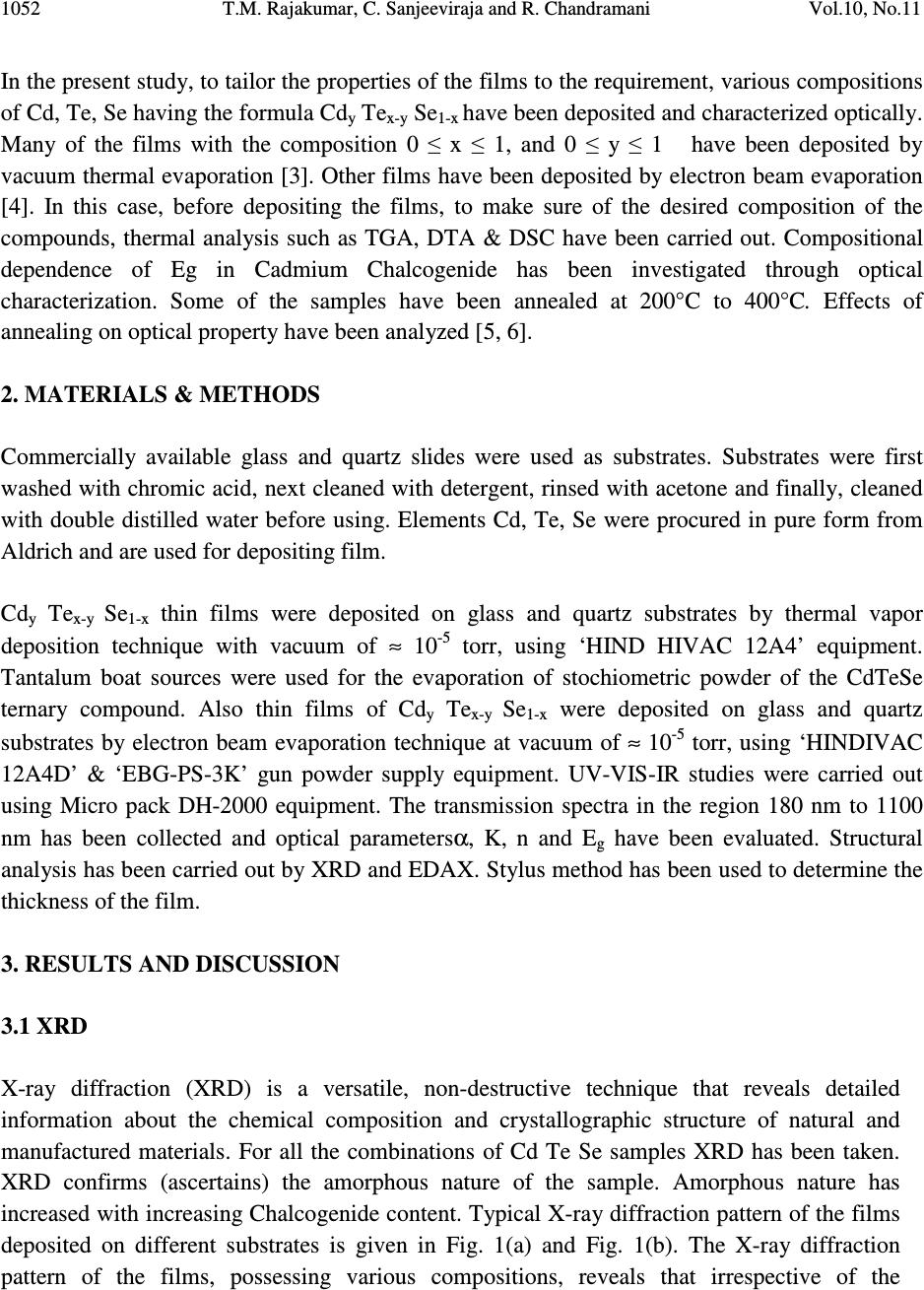 1052 T.M. Rajakumar, C. Sanjeeviraja and R. Chandramani Vol.10, No.11 In the present study, to tailor the properties of the films to the requirement, various compositions of Cd, Te, Se having the formula Cd y Te x-y Se 1-x have been deposited and characterized optically. Many of the films with the composition 0 ≤ x ≤ 1, and 0 ≤ y ≤ 1 have been deposited by vacuum thermal evaporation [3]. Other films have been deposited by electron beam evaporation [4]. In this case, before depositing the films, to make sure of the desired composition of the compounds, thermal analysis such as TGA, DTA & DSC have been carried out. Compositional dependence of Eg in Cadmium Chalcogenide has been investigated through optical characterization. Some of the samples have been annealed at 200°C to 400°C. Effects of annealing on optical property have been analyzed [5, 6]. 2. MATERIALS & METHODS Commercially available glass and quartz slides were used as substrates. Substrates were first washed with chromic acid, next cleaned with detergent, rinsed with acetone and finally, cleaned with double distilled water before using. Elements Cd, Te, Se were procured in pure form from Aldrich and are used for depositing film. Cd y Te x-y Se 1-x thin films were deposited on glass and quartz substrates by thermal vapor deposition technique with vacuum of ≈ 10 -5 torr, using ‘HIND HIVAC 12A4’ equipment. Tantalum boat sources were used for the evaporation of stochiometric powder of the CdTeSe ternary compound. Also thin films of Cd y Te x-y Se 1-x were deposited on glass and quartz substrates by electron beam evaporation technique at vacuum of ≈ 10 -5 torr, using ‘HINDIVAC 12A4D’ & ‘EBG-PS-3K’ gun powder supply equipment. UV-VIS-IR studies were carried out using Micro pack DH-2000 equipment. The transmission spectra in the region 180 nm to 1100 nm has been collected and optical parametersα, K, n and E g have been evaluated. Structural analysis has been carried out by XRD and EDAX. Stylus method has been used to determine the thickness of the film. 3. RESULTS AND DISCUSSION 3.1 XRD X-ray diffraction (XRD) is a versatile, non-destructive technique that reveals detailed information about the chemical composition and crystallographic structure of natural and manufactured materials. For all the combinations of Cd Te Se samples XRD has been taken. XRD confirms (ascertains) the amorphous nature of the sample. Amorphous nature has increased with increasing Chalcogenide content. Typical X-ray diffraction pattern of the films deposited on different substrates is given in Fig. 1(a) and Fig. 1(b). The X-ray diffraction pattern of the films, possessing various compositions, reveals that irrespective of the  Vol.10, No.11 Spectro-Structural Characterization of Chalcogenide Films 1053 deposition method and nature of substrate, the films were found to be amorphous in nature with slight shift in 2θ values shown in Table-1 [7]. Position [°2Theta] 20 30 40 5060 70 Counts 0 20 40 60 80 Sample - 1 Position [°2Theta] 20 30 4050 60 70 Counts 0 20 40 60 80 Sample - 6 Fig. 1(a) Fig. 1(b) X-ray diffraction pattern of Cd 0.8 Te 0.1 Se 0.1 X-ray diffraction pattern of Cd 0.5 Te 0.4 Se 0.1 Table – 1. Sl.No Method Composition 2θ θθ θ 1 2 3 4 5 6 7 8 9 10 Thermal evaporation Thermal evaporation Thermal evaporation Thermal evaporation Thermal evaporation Electron beam evaporation Electron beam evaporation Annealed at 200° Electron beam evaporation Annealed at 400° Electron beam evaporation Electron beam evaporation Cd 0.8 Te 0.1 Se 0.1 Cd 0.7 Te 0.2 Se 0.1 Cd 0.6 Te 0.2 Se 0.2 Cd 0.6 Te 0.3 Se 0.1 Cd 0.5 Te 0.4 Se 0.1 Cd 0.6 Te 0.2 Se 0.2 Cd 0.6 Te 0.2 Se 0.2 Cd 0.6 Te 0.2 Se 0.2 Cd 0.7 Te 0.2 Se 0.1 Cd 0.8 Te 0.1 Se 0.1 22.5° 24° 29° 23° 29° 23.5° 21.5° 21° 22° 23° 3.2 Stylus – Thickness Measurement: Thickness of the thin film is the most significant parameter, which plays important role in the properties of the thin film. Film thickness measurement (t) techniques are based on different principles such as the mass difference, light absorption, interference effects, conductivities, capacitance etc., of the films. Stylus method is a promising method to determine the thickness. The effect of applying a rounded stylus to thin metallic films on glass substrates has been investigated using diamond and steel styli with tip radii of approximately 25 µm and loadings of up to 230 g. In many applications, particularly in the case of the interference filters, an  1054 T.M. Rajakumar, C. Sanjeeviraja and R. Chandramani Vol.10, No.11 antireflection coating etc., the success of the fabrication depends only on the deposition of specific thickness of the film. The thickness of the films was estimated to be approximately 290 nm to 790 nm using the stylus surface profilometer. Measurements have been done at two or three places. The values obtained confirm the uniformity of the film. 3.3 TGA, DTA and DSC Analysis 3.3.1 TGA and DTA graphs for sample Cd 0 . 6 Te 0.2 Se 0.2 While depositing the films, to ensure the desired composition x of the compound, TGA, DTA, and DSC studies have been carried out. TGA analysis provides a quantitative measurement of any weight changes associated with thermally induced transitions. The TGA peak for the sample is shown in Fig. 2(a). In DTA, the difference in temperature between the sample and a thermally inert reference material is measured as a function of temperature. Any transition that the sample undergoes results in liberation or absorption of energy by the sample with a corresponding deviation of its temperature from that of the reference. The DTA peak for the sample is shown in Fig 2(a). In DSC, the sample and reference materials are subjected to a precisely programmed temperature change. When a thermal transition occurs in the sample, thermal energy is added to either the sample or the reference in order to maintain both the sample and reference at the same temperature. Since the energy transferred is exactly equivalent in magnitude to the energy absorbed or evolved in the transition, the balancing energy yields a direct calorimetric measurement of the transition energy. The DSC peak value for the sample is 494.43°C [Fig 2(b)]. Fig 2(a) Fig 2(b) DTA & TGA graph for sample Cd 0 . 6 Te 0.2 Se 0.2 DSC graph for sample Cd 0 . 6 Te 0.2 Se 0.2 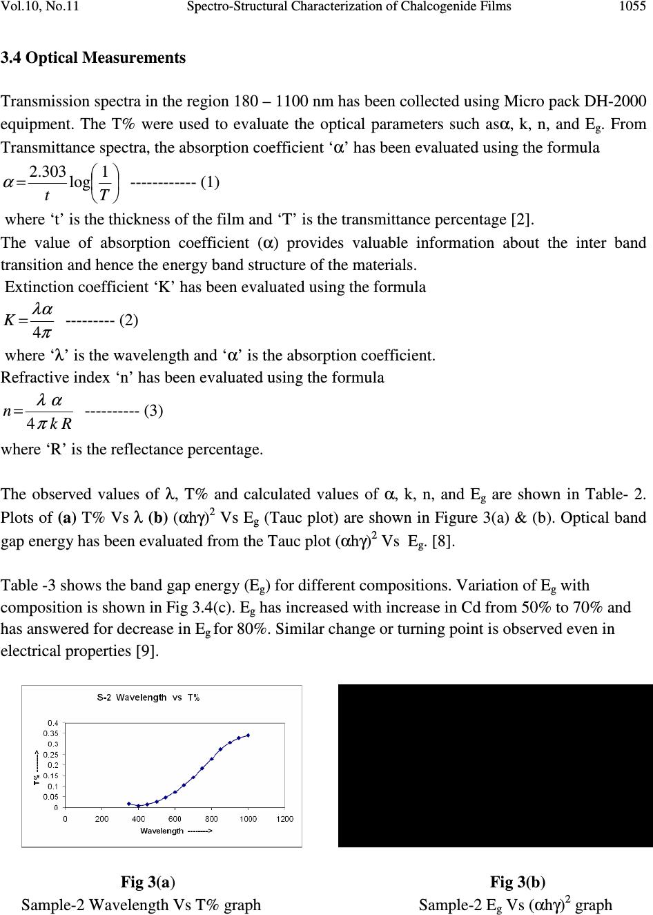 Vol.10, No.11 Spectro-Structural Characterization of Chalcogenide Films 1055 3.4 Optical Measurements Transmission spectra in the region 180 – 1100 nm has been collected using Micro pack DH-2000 equipment. The T% were used to evaluate the optical parameters such asα, k, n, and E g . From Transmittance spectra, the absorption coefficient ‘α’ has been evaluated using the formula =Tt 1 log 303.2 α ------------ (1) where ‘t’ is the thickness of the film and ‘T’ is the transmittance percentage [2]. The value of absorption coefficient (α) provides valuable information about the inter band transition and hence the energy band structure of the materials. Extinction coefficient ‘K’ has been evaluated using the formula π λα 4 =K --------- (2) where ‘λ’ is the wavelength and ‘α’ is the absorption coefficient. Refractive index ‘n’ has been evaluated using the formula Rk n π α λ 4 = ---------- (3) where ‘R’ is the reflectance percentage. The observed values of λ, T% and calculated values of α, k, n, and E g are shown in Table- 2. Plots of (a) T% Vs λ (b) (αhγ) 2 Vs E g (Tauc plot) are shown in Figure 3(a) & (b). Optical band gap energy has been evaluated from the Tauc plot (αhγ) 2 Vs E g . [8]. Table -3 shows the band gap energy (E g ) for different compositions. Variation of E g with composition is shown in Fig 3.4(c). E g has increased with increase in Cd from 50% to 70% and has answered for decrease in E g for 80%. Similar change or turning point is observed even in electrical properties [9]. Fig 3(a ) Fig 3(b) Sample-2 Wavelength Vs T% graph Sample-2 E g Vs (αhγ) 2 graph 0 10 20 30 40 50 0.000.50 1.001.502.00 2.50 3.00 3.50 ( 8 88 8 h 8 88 8 ) 2x 1 0 1 3 Eg in eV S-2 Eg vs (8 88 8h8 88 8)2 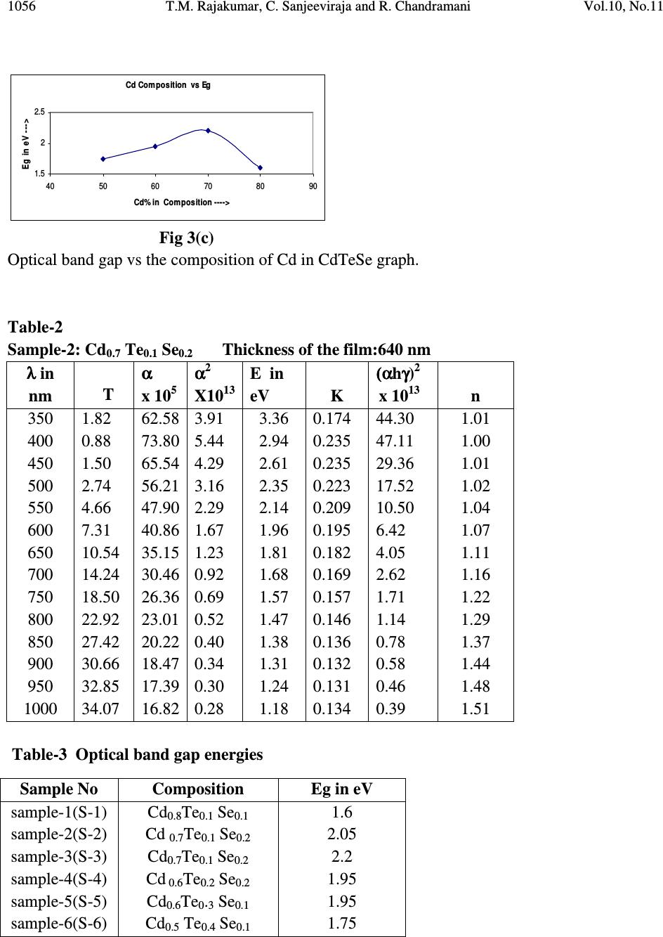 1056 T.M. Rajakumar, C. Sanjeeviraja and R. Chandramani Vol.10, No.11 Cd Composition vs Eg 1.5 2 2.5 4050 6070 8090 Cd% in Composition ----> Eg in eV ---> Fig 3(c) Optical band gap vs the composition of Cd in CdTeSe graph. Table-2 Sample-2: Cd 0.7 Te 0.1 Se 0.2 Thickness of the film:640 nm λ λλ λ in nm T α αα α x 10 5 α αα α 2 X10 13 E in eV K ( (( (α αα α h γ γγ γ ) 2 x 10 13 n 350 400 450 500 550 600 650 700 750 800 850 900 950 1000 1.82 0.88 1.50 2.74 4.66 7.31 10.54 14.24 18.50 22.92 27.42 30.66 32.85 34.07 62.58 73.80 65.54 56.21 47.90 40.86 35.15 30.46 26.36 23.01 20.22 18.47 17.39 16.82 3.91 5.44 4.29 3.16 2.29 1.67 1.23 0.92 0.69 0.52 0.40 0.34 0.30 0.28 3.36 2.94 2.61 2.35 2.14 1.96 1.81 1.68 1.57 1.47 1.38 1.31 1.24 1.18 0.174 0.235 0.235 0.223 0.209 0.195 0.182 0.169 0.157 0.146 0.136 0.132 0.131 0.134 44.30 47.11 29.36 17.52 10.50 6.42 4.05 2.62 1.71 1.14 0.78 0.58 0.46 0.39 1.01 1.00 1.01 1.02 1.04 1.07 1.11 1.16 1.22 1.29 1.37 1.44 1.48 1.51 Table-3 Optical band gap energies Sample No Composition Eg in eV sample-1(S-1) sample-2(S-2) sample-3(S-3) sample-4(S-4) sample-5(S-5) sample-6(S-6) Cd 0.8 Te 0.1 Se 0.1 Cd 0.7 Te 0.1 Se 0.2 Cd 0.7 Te 0.1 Se 0.2 Cd 0.6 Te 0.2 Se 0.2 Cd 0.6 Te 0 . 3 Se 0.1 Cd 0.5 Te 0.4 Se 0.1 1.6 2.05 2.2 1.95 1.95 1.75 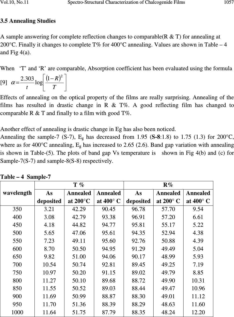 Vol.10, No.11 Spectro-Structural Characterization of Chalcogenide Films 1057 3.5 Annealing Studies A sample answering for complete reflection changes to comparable(R & T) for annealing at 200°C. Finally it changes to complete T% for 400°C annealing. Values are shown in Table – 4 and Fig 4(a). When ‘T’ and ‘R’ are comparable, Absorption coefficient has been evaluated using the formula [9] ( ) − =T R t 2 1 log 303.2 α Effects of annealing on the optical property of the films are really surprising. Annealing of the films has resulted in drastic change in R & T%. A good reflecting film has changed to comparable R & T and finally to a film with good T%. Another effect of annealing is drastic change in Eg has also been noticed. Annealing the sample-7 (S-7), E g has decreased from 1.95 (S-8:1.8) to 1.75 (1.3) for 200°C, where as for 400°C annealing, E g has increased to 2.65 (2.6). Band gap variation with annealing is shown in Table-(5). The plots of band gap Vs temperature is shown in Fig 4(b) and (c) for Sample-7(S-7) and sample-8(S-8) respectively. Table – 4 Sample-7 T % R% wavelength As deposited Annealed at 200°C Annealed at 400° C As deposited Annealed at 200° C Annealed at 400° C 350 400 450 500 550 600 650 700 750 800 850 900 950 1000 3.21 3.08 4.18 5.65 7.23 8.70 9.82 10.54 10.97 11.27 11.55 11.69 11.70 11.64 42.29 42.79 44.82 47.06 49.11 50.50 51.00 50.74 50.20 50.10 50.52 50.99 51.36 51.75 90.45 93.38 94.77 95.61 95.60 94.95 94.06 92.81 91.15 89.68 89.03 88.87 88.39 87.79 96.78 96.91 95.81 94.35 92.76 91.29 90.17 89.45 89.02 88.72 88.44 88.30 88.29 88.35 57.70 57.20 55.17 52.94 50.88 49.49 48.99 49.25 49.79 49.90 49.47 49.01 48.63 48.24 9.54 6.61 5.22 4.38 4.39 5.04 5.93 7.19 8.85 10.31 10.96 11.12 11.60 12.20  1058 T.M. Rajakumar, C. Sanjeeviraja and R. Chandramani Vol.10, No.11 S-7 Wavelength vs R & T % 40 60 80 100 02004006008001000 1200 Wavelength R% & T% R%- As depositedR%-Anneald at 200°C T%-Anneald at 200°CT%-Anneald at 400°C Fig 4(a) S-7 Wavelength Vs R & T%. S-8 Variation of band gap energy with annealing As deposited Annld at 200 0 C Annld at 400 0 C 0 0.5 1 1.5 2 2.5 3 Temperat ure Band gap energy Fig 4(b) Fig 4(c) S-7 Variation of band gap with annealing. S-8 Variation of band gap with annealing. Table-5. Band gap variations. Optical Band gap in eV Sample Composition As Deposited Annealed at 200 0 C Annealed at 400 0 C S-7 S-8 Cd 0.6 Te 0.2 Se 0.2 Cd 0.7 Te 0.2 Se 0.1 1.95 1.8 1.75 1.3 2.65 2.6 As deposited Annld at 200 0 C Annld at 40 0 0 C 0 0.5 1 1.5 2 2.5 3 B a n d g a p e n e r g y T emperature S-7 Variation of band gap with annealing  Vol.10, No.11 Spectro-Structural Characterization of Chalcogenide Films 1059 4. CONCLUSIONS Cd chalcogenides for various compositions, 0 ≤ x ≤ 1 and 0 ≤ y ≤ 1 were prepared by thermal evaporation as well as by electron beam evaporation. • XRD has confirmed the amorphous nature of the films. • Uniformity of the films has been confirmed by Stylus measurement. • Dependence of band gap with the composition has been justified by optical studies. • Transmittance percentage has varied from 0.889 to 34.09 for Cd varying in the range 0 ≤ x ≤ 1. • Increase in Cd has resulted in increase of E g which is a cumulative effect of the increase of Cd along with decrease in Se. • Annealing at 200°C has resulted in decrease of E g . • Effects of annealing on the optical property of the films are really surprising. Annealing of the films has resulted in drastic changes in the optical properties. • Drastic change in E g also been noticed after annealing at 200°C and 400°C. • Study reveals that slow rate changes occurring at low temperature ranges 200°C to 400°C can be used to control the optical/electrical property and finally optical band gap in a precise manner. • Further work to confirm the exact turning point in E g is in progress. ACKNOWLEGMENT The authors thank Dr.Premachandra Sagar, Vice Chairman, Dayananda Sagar Institutions, Bangalore, India for his continuous encouragement. REFERENCES [1] R. Bhargava, Properties of wide band gap II-VI semiconductors. (1997) (INSEOSEC) publications, London. [2] C. Baban, G.I. Rusuand Prepelita (2005) Journal of Opto Electronics and Advanced Materials Vol 7(2) pp.817-821. [3] P.J. Sebastian and S. Sivaramakrishnan, Journal of Applied Physics, 65, 237(1989). [4] R. Islam, H.D. Banergee, D.R.Rao, (1995) Thin Solid Films Vol.266, pp.215. [5] Uma and R. Chandramani (2009) J. of Active and Passive Electronic Devices, Vol.8, pp.213-222. [6] Jaan Hiie, -Article, Tallinn University of Technology, Department of Materials Science, Chair of Semi-conducting Materials Technology ,Ehitajate tee 5 19086 Tallinn, Estonia. Energy and Power Newsletter Vol.4 Issue 11 [7] D. Cullity, Elements of x-ray diffraction, (1959) Addison Wesley Press, London .  1060 T.M. Rajakumar, C. Sanjeeviraja and R. Chandramani Vol.10, No.11 [8] Tauc, J. (1968) “Optical properties and electronic structure of amorphous Ge and Si”. Material Research Bulletin Vol.3: pp.37-46. [9] T. Bhuvaneshwara Babu, R. Chandramani (2009) “ Growth & Optical Characterization of Ternary Materials”, Journal of Research & Industry, Vol. 2, pp. 91-96. |