Int'l J. of Communications, Network and System Sciences
Vol.2 No.5(2009), Article ID:595,14 pages DOI:10.4236/ijcns.2009.25036
TDTL Based Frequency Synthesizers with Auto Sensing Technique
College of Engineering, Khalifa University of Science, Technology and Research, Sharjah Campus, Sharjah, UAE
Email: mqutayri@kustar.ac.ae
Received March 7, 2009; revised April 12, 2009; accepted May 20, 2009
Keywords: Time-Delay Tanlock Loop, Frequency Synthesizer, Phase Lock Loop, Indirect Synthesis
ABSTRACT
This paper presents a frequency synthesizer architecture based on the time delay digital tanlock loop (TDTL). The loop is of the first order type. The synthesizer architecture includes an adaptation mechanism to keep the complete system in lock. The mechanism uses a frequency sensing structure to control critical TDTL parameters responsible for locking. Both integer and fractional multiples of the loop reference frequency are synthesized by the new architecture. The ability of the TDTL based frequency synthesizer to respond to sudden variations in the system input frequency is studied. The results obtained indicate the proposed synthesizer has a robust performance and is capable of responding to those changes provided that they are within the bounds of its locking region.
1. Introduction
The explosion in the growth of communication systems in general and wireless ones in particular is placing highly demanding requirements on the designers of such systems. Modern wireless communication systems have to support high data rates with low power consumption, high signal to noise ratios and compact designs. In addition to this, wireless systems must be able to deal with different communication standards operating at various frequencies [1-3]. The frequency synthesizer is one of the fundamental components of any wireless transceivers. As shown in Figure 1, the frequency synthesizer is basically a device that generates any number of operating frequencies (Fout) from a stable input reference frequency (Fref) under the control of a command word or signal (fc).
In wireless communication system transceivers frequency synthesizers are used as the local oscillators to generate the periodic signals required for the up-conversion as well as down-conversion processes [4-7]. Figure 2 shows the generic architecture of a wireless RF (radio frequency) transceiver with the frequency synthesizer block.
Depending on the process of frequency generation, frequency synthesizers are classified as direct or indirect [7,8]. Direct frequency synthesis can be divided into coherent and incoherent types. In the latter, synthesis is achieved by using fixed oscillators in addition to a group of frequency dividers and multipliers in order to generate
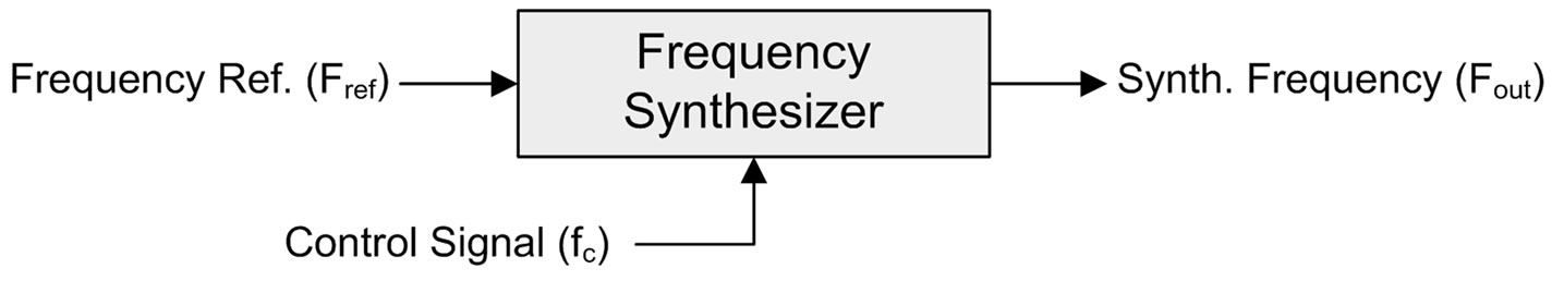
Figure 1. Frequency synthesis process.
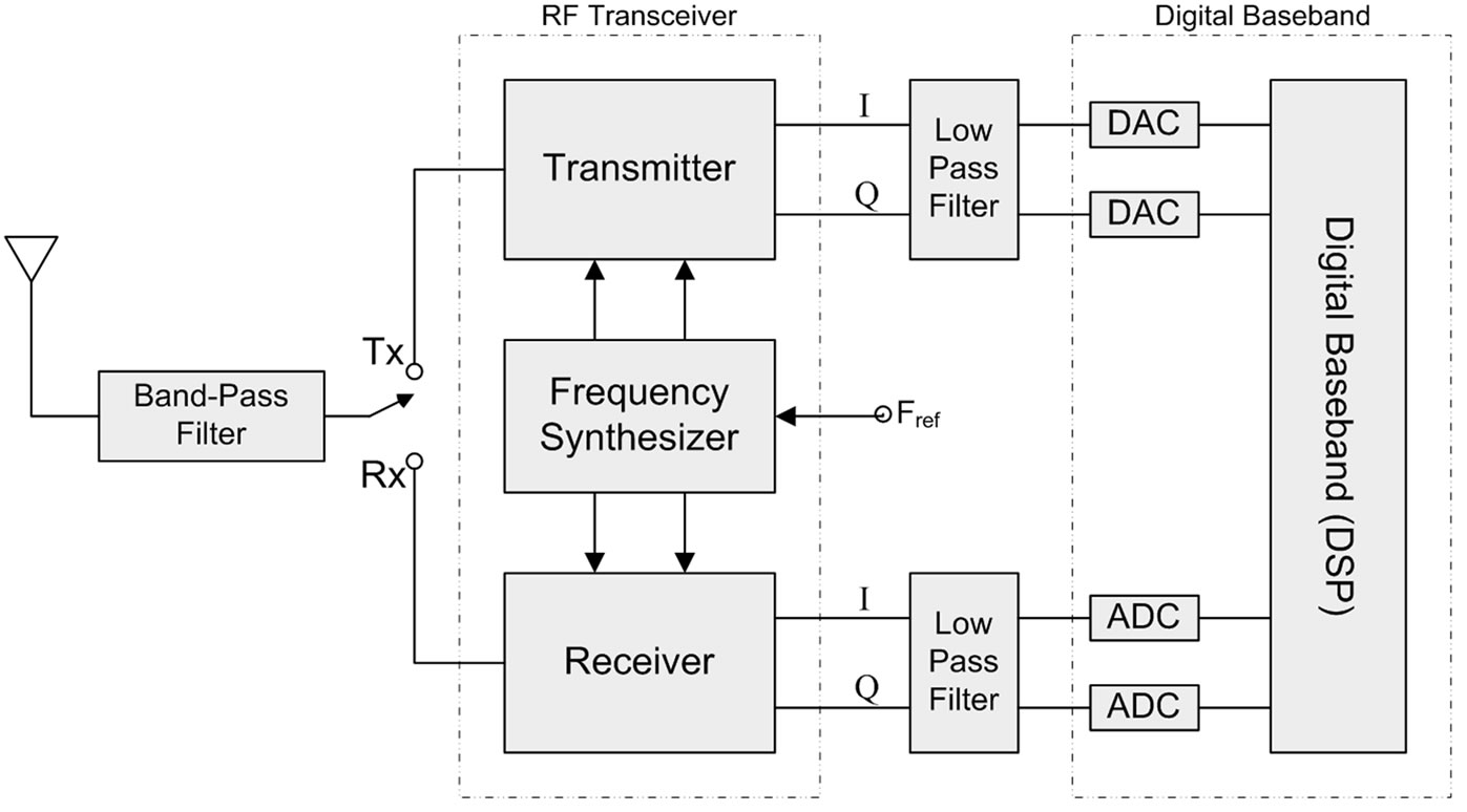
Figure 2. Basic transceiver architecture.
Figure 3. Basic indirect frequency synthesizer.
a variety of frequencies. In the coherent technique, however, only one reference source is used to generate the required output frequencies. In this approach, the stability and accuracy of the output frequencies are the same as that of the reference source. One example of the coherent technique is the phase accumulation synthesizer. The main advantages of the direct synthesis are the fast settling, fine step sizes, and simple implementation. The disadvantages of this technique are bandwidth limitations and undesired spurious harmonic generation. These problems pose severe limitations on future generation wireless communications such as 4G where OFDM is employed [7-10].
The second approach in frequency synthesis is the indirect frequency synthesis. The theory behind this type of synthesis is that it uses an unstable oscillator; the oscillator is then forced to be stabilized by feeding back a portion of the received (original) signal. The feedback is used to stabilize the loop as well as provide enough information in order to reconstruct the signal by generating a replica of the carrier [5,7,11-13]. The advantages of using such technique are the generation of spurious free output signals, the wideband system operation, and the less stringent requirement on the local oscillator frequency stability. The main limitations are the settling time and phase noise which can be minimized by using additional circuitry embedded in the loop. Two approaches of the indirect synthesis are the analog PLL synthesizer and the digital PLL synthesizer. The basic block diagram of an indirect frequency synthesizer is depicted in Figure 3.
This paper uses a novel type of digital phase lock loops called the time-delay digital tanlock loop (TDTL) as the locking element of the indirect frequency synthesizer system. The TDTL is a high performance phase locking system that can be implemented efficiently as all its components are of the digital type [14].
The paper is organized as follows. Section 2 presents the architecture and system equations of the time-delay digital tanlock loop. This also includes the locking range of the TDTL which is a major aspect of a phase lock loop. Section 3 discusses the process and the challenges of using the TDTL as a frequency synthesizer. The adaptation process introduced to enable the TDTL based frequency synthesizer to achieve locking for both integer and fractional frequency division is also detailed in Section 3. The results of the new TDTL based frequency synthesizer for various division factors and under different input conditions are presented in Section 4. The conclusions of this work are presented in Section 5.
2. Time-Delay Digital Tanlock Loop
The structure of the TDTL is shown in Figure 4. It consists mainly of two sample and hold blocks, a phase detector, a low pass filter, a digitally controlled oscillator, and a time-delay block. Being comprised of these components, the TDTL lends itself for implementation in various digital systems technologies. The TDTL offers an inexpensive implementation and improved performance compared with other synchronization techniques. Compared with the conventional digital tanlock loop in [15], the TDTL in Figure 4 does not preserve the linearity of the phase characteristics. This is due to the fact that the delay component of the loop is frequency dependent and hence causes the phase shift of the input signal to deviate somewhat from the original designed value over the locking range. Consequently an element of nonlinearity is introduced into the locking range. However, this supposed disadvantaged can basically be ignored because the TDTL preserves the wide locking range and fast acquisition behavior advantages of the conventional digital tanlock loop and uses a system architecture that is easier to implement in hardware compared to the conventional type. An in depth comparison of the conventional digital tanlock loop and TDTL with extensive results and discussion is given in [16]. The mathematical analysis of the TDTL under noise free conditions is detailed below. All of the signal notations are chosen in reference to the block diagram shown in Figure 4. The analysis follows a similar line to that given in [14,17,18].
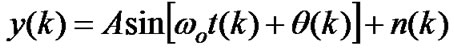
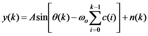
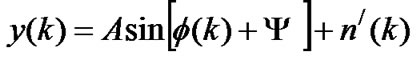
The TDTL receives a continuous time sinusoid y(t) which is given by (1).
 (1)
(1)
where A is the amplitude of the signal,  is the free running frequency of the DCO,
  is the information-bearing phase and
  is the additive white Gaussian noise (AWGN). The signal is assumed not to have a DC component. Usually the phase process
  is a translation of frequency or phase steps.
 ![]() is the radian frequency of the input signal and
is the radian frequency of the input signal and  is a constant. A phase lag
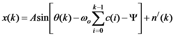
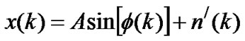
  is induced to the input signal after it passes through the time delay block. Therefore, x(t) is generated, which is a phase shifted version of the input signal y(t), this signal is given by (2).
 (2)
(2)
where  is the time-delayed AWGN due to
![]() . The aforementioned continuous time signals pass to the sample and hold blocks, and thereby get transformed to the discrete time signals in (3) and (4).
. The aforementioned continuous time signals pass to the sample and hold blocks, and thereby get transformed to the discrete time signals in (3) and (4).
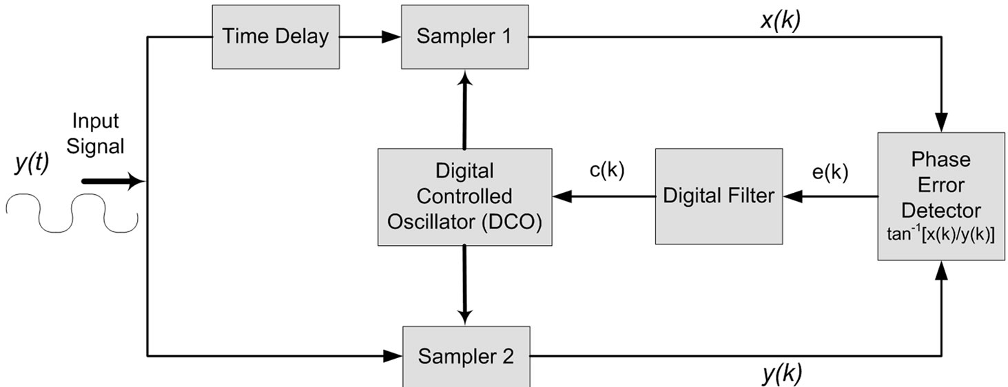
Figure 4. Architecture of time-delay digital tanlock loop.
 (3)
(3)
 (4)
(4)
where .
.
The sampling interval between the sampling instants  and
and  is given by (5).
 (5)
(5)
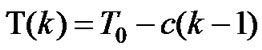
where 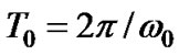 is the nominal period of the DCO and
  is the output of the digital filter at the ith sampling instant. Assuming
 , the total time
  elapsed up to the kth sampling instant is given by (6).
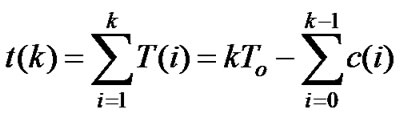 (6)
(6)
 (7)
(7)
 (8)
(8)
And therefore, the phase error between the input signal and the DCO can be also defined as:
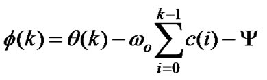 (9)
(9)
Having defined the phase error, Equations (7) and (8) can be rewritten as
 (10)
(10)
 (11)
(11)
These signals are applied to the phase detector producing the error signal  given in (12).
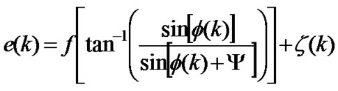 (12)
(12)
where ,
,  is a random phase disturbance due to AWGN. The error signal
  represents a nonlinearly mapped version of the phase error. However, the effect of the nonlinearity is minimum and e(k) can be approximately linear if
  is equal to, or in the vicinity of π/2. This relatively small effect of nonlinearity is illustrated in Figure 5 by the plot for Y0=p¤2, which can be reconstructed as a pricewise linear one. The digital filter, which has a transfer function given by
  receives the error signal e(k) and produces the signal
  that drives the DCO. Therefore, the system difference equation can be derived from (6) and (9) as
 (13)
(13)
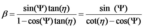
where , and the AWGN terms are neglected since noise-free analysis is assumed. In the case of the conventional digital tanlock loop, the linear characteristic function of the phase detector enables the description of the loop as a linear difference equation, and hence finding the lock range using the stability criterions of its Z-transformed transfer function [15]. However, the nonlinear characteristic function of the TDTL phase detector results in a nonlinear difference equation, which can only be solved by numerical analysis. The lock range of the TDTL was analyzed in [14], using fixed-point theorems, which have been utilized previously in the analysis of the lock range of sinusoidal ZC-DPLLs [19,20]. The digital filter of the first order loop is simply a gain block G1, and the system equation is given by
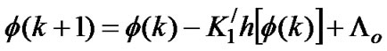 (14)
(14)
where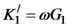 . Defining
  as
as  will result in
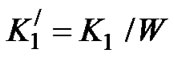 , where
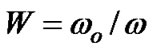 . The nominal phase lag
  induced by the time delay units on the input can be initially arranged by manipulating the parameters
  and
and  in the manner given by
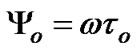 . Therefore, the locking range can be acquired by numerically solving the inequality
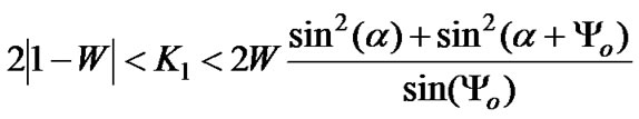 (15)
(15)
where  ,
,
 and
and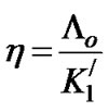
One of the properties of the first order TDTL is that it converges to a nonzero steady state phase error, which is translated with a phase offset between the pulses of the DCO and the zero crossings of the input signal. The steady-state value of the phase error is given by  where
where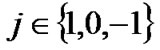 . Figure 5 shows the locking range of the first-order TDTL for different values of
  as well as the conventional digital tanlock loop locking region [14].
The range of independent locking of the TDTL and the effect of initial phase error are studied in depth in [14,21].
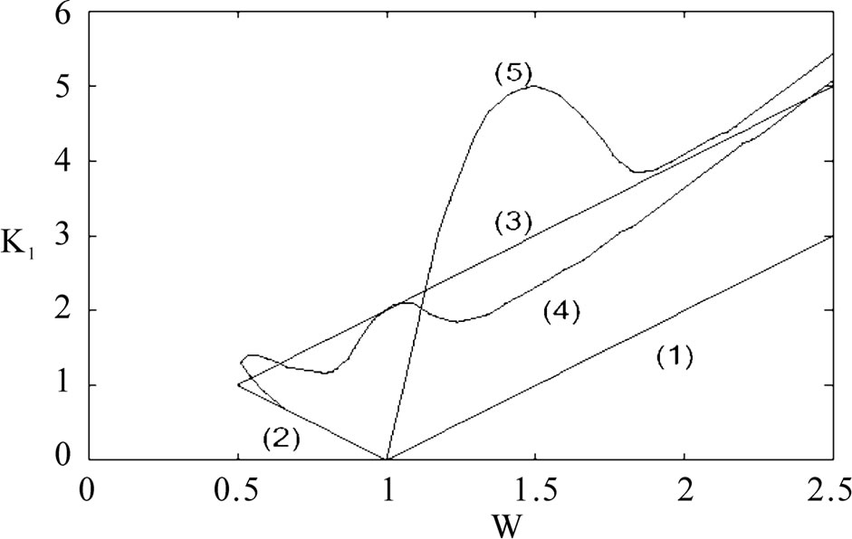
Figure 5. Major locking range of the 1st TDTL for different values of Y0=w0t. Note: the region enclosed by (1), (2) and (3) is for the conventional digital tanlock loop; the region enclosed by (1), (2) and (4) is for the TDTL when Y0=p¤2; and the region enclosed by (1) and (5) is for the TDTL when Y0=p.
Figure 6. Structure of the TDTL frequency synthesizer.
Since the TDTL has non-linear characteristic function numerical analysis were used to determine the range of independent locking. The analysis shows that the TDTL offers an advantage on the conventional digital tanlock loop in this regard.
3. TDTL Frequency Synthesizer
As shown in Figure 6, the TDTL based Synthesizer is mainly comprised of two subsystems; namely the first order TDTL and the frequency divider. The two subsystems are configured to form an indirect frequency synthesizer. The divider generates various frequencies which are multiple of the DCO frequency, while the TDTL locks and stabilizes the synthesized frequency. This section gives a general overview of the synthesizer system that includes the operation of the TDTL and the divider as a frequency synthesizer block. Depending on the desired division factor, the synthesizer may be classified as an integer one or a fractional one. Both classes are discussed below.
3.1. Integer TDTL-FS
In this paper the TDTL is utilized to act as an indirect frequency synthesizer as depicted in Figure 6. This is so because the different frequencies that are produced in loop or in other words the frequency division operation are occurring within the feedback path of the loop. To achieve frequency division, a counter is introduced into the loop. This counter is placed between the DCO and the Sample and Hold blocks. Therefore, now the sampling frequency of the loop is not the frequency of the DCO but the output of the divider or the counter.
The operation of frequency division is simple in which a counter is used that is clocked with the input signal. The counter has a limited number of states or counts that are equal to the division factor that is required. For example, in a divide by 2 cases the counter has 2 states (i.e. 2 counts) and produces an output when it reaches the final state before it resets i.e. it will count from 0 to 1 and will produce an output while it is residing at 1. In other words, the counter will produce 1 pulse for every 2 pulses in the case of a divide by 2 counters. Generally speaking, a divide by N counter will produce 1 pulse as an output for every N counts or input pulses, hence divide by N.
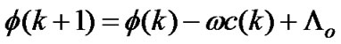
Following the introduction of the divider into the system, it was observed that the system response has changed, in which, for the same loop conditions, the system would go out of lock when the divider is introduced and would stabilize and lock if the divider is removed. Analysis of the system and associated problems indicated that the introduction of the divider into the system has the effect of moving the operating point of the system outside the locking range of the system. The reason for this is that the sampling frequency of the S/H blocks has decreased. Therefore, to compensate for this, the DCO frequency was multiplied by the same factor (N) in order to achieve the original sampling frequency. Another interesting point that was found is that in order to get the system back into its exact original operating point, not only the DCO frequency has to be adjusted but also the error signal that is fed to the DCO from the phase error detector had to be adjusted too.
The divider block has the effect of dividing the frequency of the DCO output which is considered to be a result of two factors, the DCO running frequency and the error signal. Therefore, when the output of the DCO is divided not only the frequency is divided but also the effect of the error signal that feeds the DCO and its weight (original value) in the system. As a result, both the DCO running frequency and the error signal have to be conditioned and adjusted when the divider is introduced into the system. The adjustments are done by multiplying the error signal and the DCO running frequency by the same division factor in order to get the system back into its original operating point. For example, as illustrated in Figure 7, the TDTL was configured to operate at point A within the locking range, where W=w0/w=1 and K=Gw0=1, prior to the introduction of the divider.
After introducing the divider (÷N) and depending on the division factor, the operating point may shift outside the locking range towards point B, Figure 7. This is because the error signal effect will be divided by N and hence the output of the gain block will be divided by N as well as the DCO frequency and the new operating point will be at W¢=w0/Nw=1/N and K¢=Gw0/N2=1/N2. So, in order to get the system back in lock, the DCO frequency w0 and the Gain G are multiplied by the same division factor and this will bring the system back into its original state.
As stated above, the TDTL synthesizer requires some adjustments after introducing the divider in order to keep the loop locked in its basic original operating point. These adjustments are basically adjusting the DCO frequency and the error signal. In order to make this process as flexible as possible, an adaptation mechanism is introduced in the system. The mechanism basically cancels the effect of the division on the system stability through adjustment of some system parameters. This mechanism
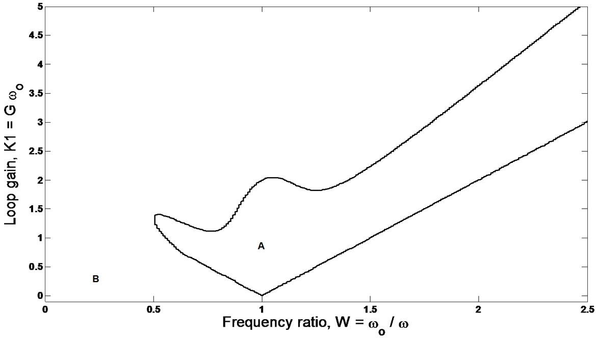
Figure 7. Locking range of first-order TDTL.
 (a)
(a)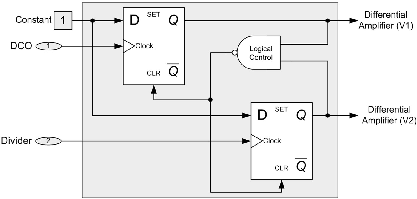 (b)
(b)
Figure 8. (a) Block diagram of frequency sensing block (b) Structure of the frequency detector.
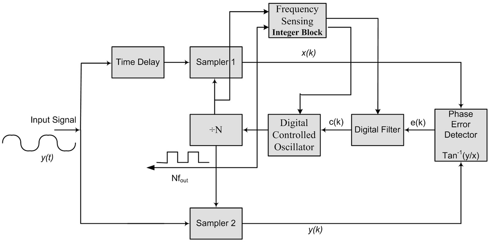
Figure 9. Structure of integer TDTL-FS with FSB.
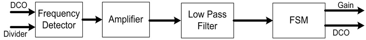
is mainly composed of a frequency sensing block (FSB). The frequency sensing block consists of a frequency detector, a filter block, a differential amplifier and a finite state machine (FSM). The structure of the FSB and the frequency detector are shown in Figure 8a and Figure 8b respectively. The integer TDTL-FS incorporating the adaptive FSB to keep it stable is depicted in Figure 9.
The basic functionality of the FSM block of the FSB is to compare between the two frequencies at the input of the divider and its output and produce an output (train of pulses with certain widths) that corresponds to the difference in frequency. This output is fed into an amplifier and then to a low pass filter in order to extract the required information. The extracted information will be in the form of a certain DC value, and this value is then fed into the FSM in order to be conditioned and to get a suitable output for adapting the system. The output of the FSM is used to adjust the gain of the variable gain block G in the loop and the frequency of the DCO. The synthesizer structure uses a variable gain block G that makes the adaptation process possible.
3.2. Fractional TDTL-FS
Fractional synthesizers are the type of systems that can produce not only integer multiple (÷N) of the source frequency but also a fractional multiple (÷N.p) of it. The fractional synthesizer basically uses a type of fractional dividers and employs it to produce fractional divisions. The fractional divider can be constructed using different methods. In this paper a modulus-2 prescaler divider was designed and subsequently introduced into the system. This type of fractional divider uses two integer dividers that are controlled by a control unit. The inputs of the control unit are driven by the outputs of the two dividers in order to generate the signal that controls the MUX and DeMUX blocks. This control unit is the one responsible for creating the fraction part of the division. The two integer dividers have to be increments of each other i.e. 5 and 6 or 7 and 8 etc, in general P/P+1. The block diagram of the modulus-2 prescaler is shown in Figure 10.
As discussed in the previous integer divider section, introducing a divider into the TDTL will cause some changes in the performance of the system that requires certain adjustments. Similarly, introducing a fractional divider requires employing the same adaptation principle; however the case now is more difficult because of the use of two independent dividers as well as a control mechanism that switches between these two dividers.
Before applying an adaptation mechanism, the loop was tested and analyzed after introducing the fractional divider. After different assessments, it was found that in the case of a fractional divider, the operating point of the loop does not shift outside the locking range into one single location but oscillates between two different locations.
Each division factor is responsible for shifting the operating point to one of the points. Therefore, in order to get the loop back into its nominal point, point A in Figure 7, the adaptation process has to compensate for the two divisions individually and one at a time. This observation implied that a more complex adaptation process is required that has the ability to adapt the system for two division factors and switch quickly between them as the control unit switches between the two dividers.
As a solution to the previous problems, duplicate blocks were added to the fractional divider that were used to condition the divider in such a way that it is now possible to extract the required information about the division factor. This approach includes duplicating the two dividers and using the duplicates as dummy counters that have access to the input signal all the time, not switched inputs, and two FSBs connected to those two counters. The outputs of the two FSBs are switched using a demultiplexer that is controlled by the same output of the control unit of the fractional divider. The block diagram of the adaptation process is shown in Figure 11 and the complete fractional TDTL-FS is depicted in Figure 12. The advantage of this approach is that the switching between the two adaptation signals from FSB1 and FSB2 is switched simultaneously with the switching of the division because they are both taking their switching signal from the same control unit.
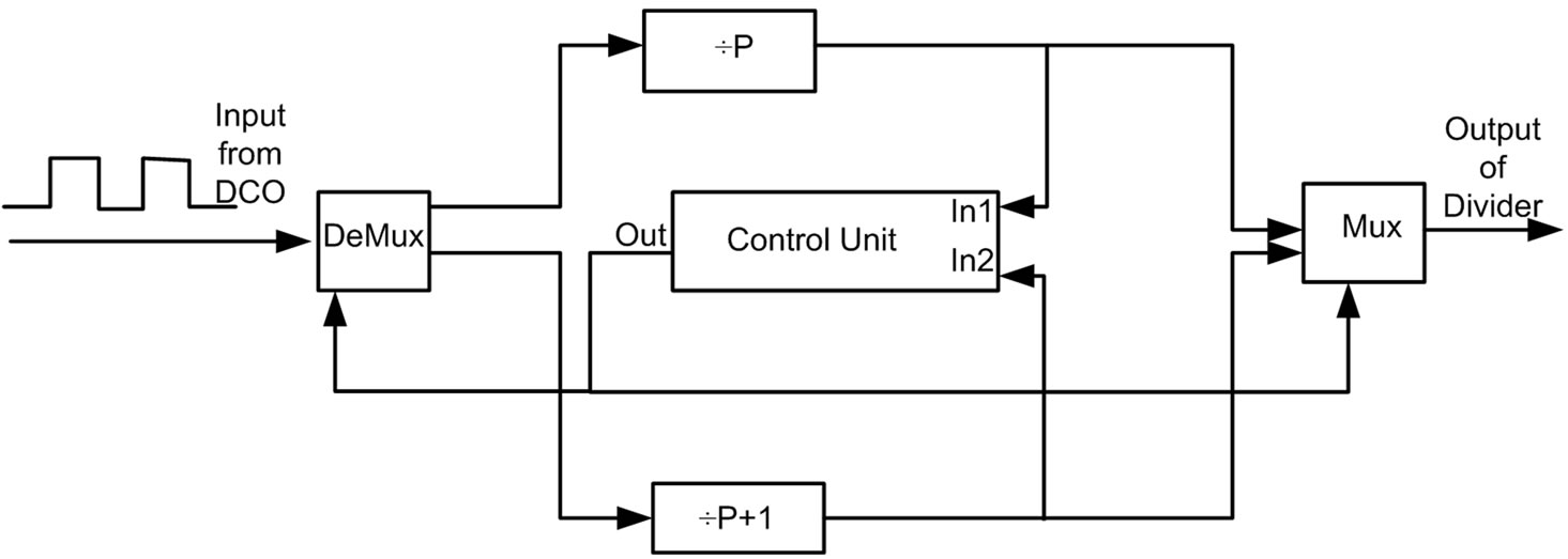
Figure 10. Modulo-2 prescaler divider.
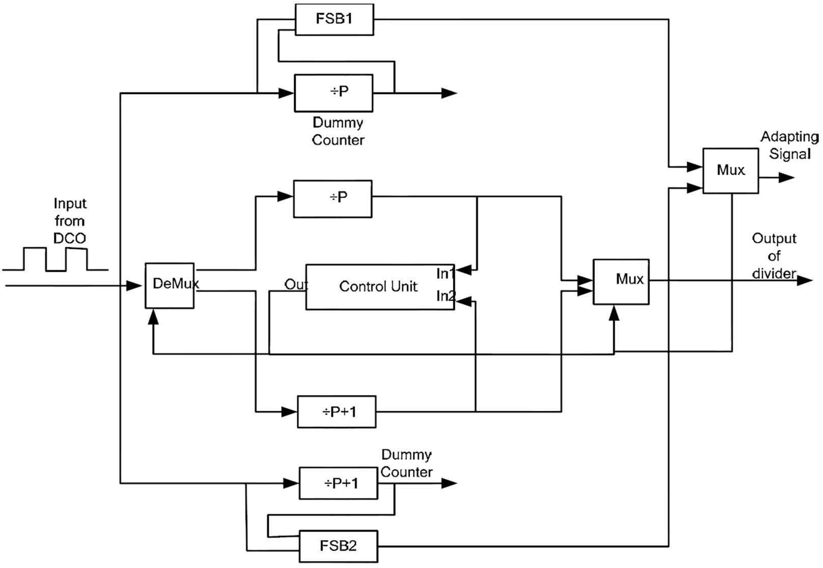
Figure 11. Adaptation mechanism for fractional divider in TDTL-FS using FSB.
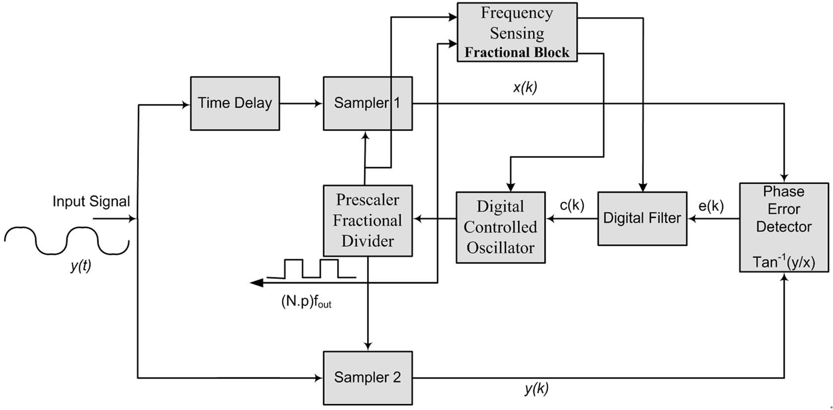
Figure 12. Structure of fractional TDTL-FS with FSB.
4. TDTL-FS Results
This section presents the simulation results of the TDTL frequency synthesizers for both integer and fractional divisions. The TDTL used in both cases is of the firstorder type. The modeling, simulation, and testing of all system architectures were done using MATLAB/SIMULINK. The results in this section illustrate the ability of the TDTL frequency synthesizers to regain its locking state following the introduction of the division process into the loop. They also show that the system is capable of synthesizing frequencies that are integer as well as fractional multiples of the input frequency.
4.1. Integer Division
After applying the divider into the system, several input steps were subjected to the system. A positive step indicates an increase in the input frequency while a negative step indicates a decrease in the input frequency. In all cases and prior to the introduction of the division process the loop was chosen to operate at point A in Figure 7, which is considered the optimum point in the locking range as it allows symmetrical swing in the input signal. At point A the frequency ratio is W=ωo/ω=1 and K= Gωo= 1. The time delay was chosen to be ψo=ωoτ = π/2. These conditions imply that the TDTL basic system is in lock.
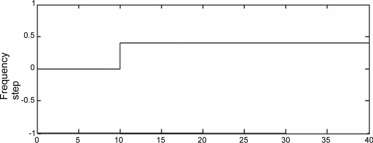
An example of applying a positive step to a TDTL-FS with and integer divider is shown in Figure 13. Figure 13(a) shows the input step with amplitude of 0.4 and system response in Figure 13(b) and Figure 13(c) prior to the incorporation of the FSB adaptation block. It can be clearly seen that the TDTL-FS is out of lock. Figure 13(c) depicts the phase plane response of the system which clearly shows the lack of convergence. The arrow in the figure indicates f(0). The effect of the FSB on the stability of the TDTL-FS is shown in Figure 13(d). It can be seen that the system regained lock following the activation of the FSB block. Once the system stabilized it was able to generate correct integer division. This is illustrated in Figure 14 for a division factor of 16.
4.2. Fractional Division
The concept of TDTL-FS fractional synthesis using the FSB approach was achieved and simulated. An input with a positive frequency step was applied to the system. The system response to that step is shown in Figure 15. It can be clearly seen that the system locks onto the input but with a steady state error. The error does not converge to zero due to the limitations of the order of the loop filter, in which a simple gain block is used as the loop filter.
 (a)
(a)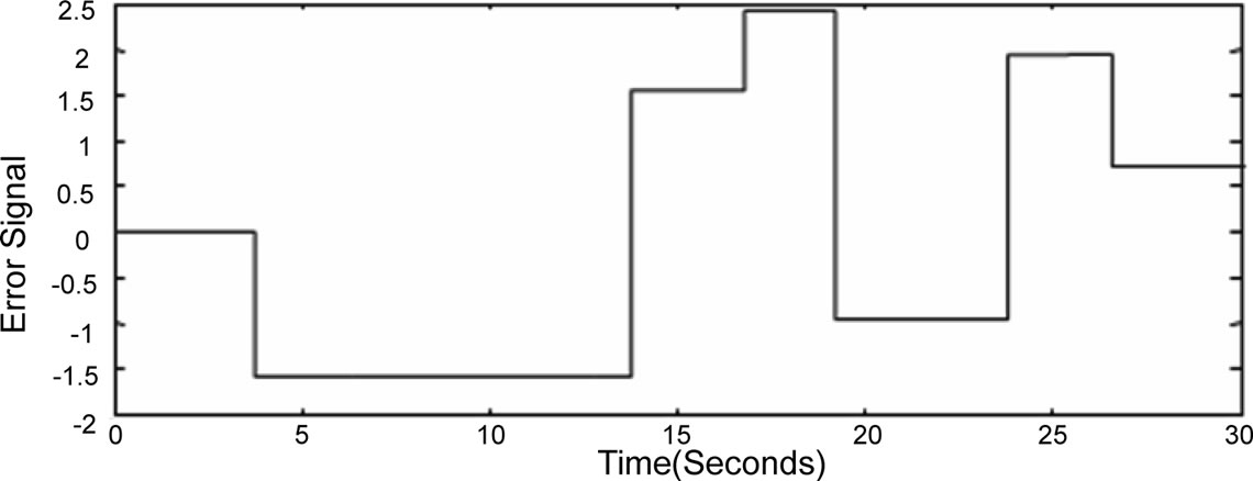 (b)
(b) (c)
(c)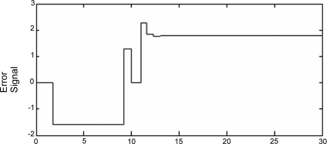 (d)
(d)
Figure 13. TDT-FS system response for integer division (a) Positive step input, (b) Phase error without adaptation, (c) Phase plane without adaptation (d) Phase error with adaptation.
It is important to mention that the response of the system to the frequency step is very similar to the response of the loop itself, this implies and proves that, in both cases, the system is operating at the same operating point. This observation concludes that the adaptation mechanism was successful in adjusting the loop and shifting it back into its original location. However, it is also important to point that the system adaptation using the FSB approach requires about 15 samples to initialize it and be able to adapt the system, and this is one of the disadvantages of this approach.
The division factor that was chosen for this simulation example was (÷3.25). The frequency division that was achieved for this example is shown in Figure 16. It can be clearly seen that the division cycles are broken into four parts, for the first three parts the input is divided by 3 and for the last part the input is divided by 4 and hence a division by 3.25 is achieved.
5. Conclusions
The TDTL is an efficient mixed-signal digital phase lock loop. This paper presented the architecture and governing system equations of the TDTL. It then presented a novel indirect frequency synthesis system based on the TDTL. The system shows a robust performance as it deals with sudden changes in the input signal frequencies.
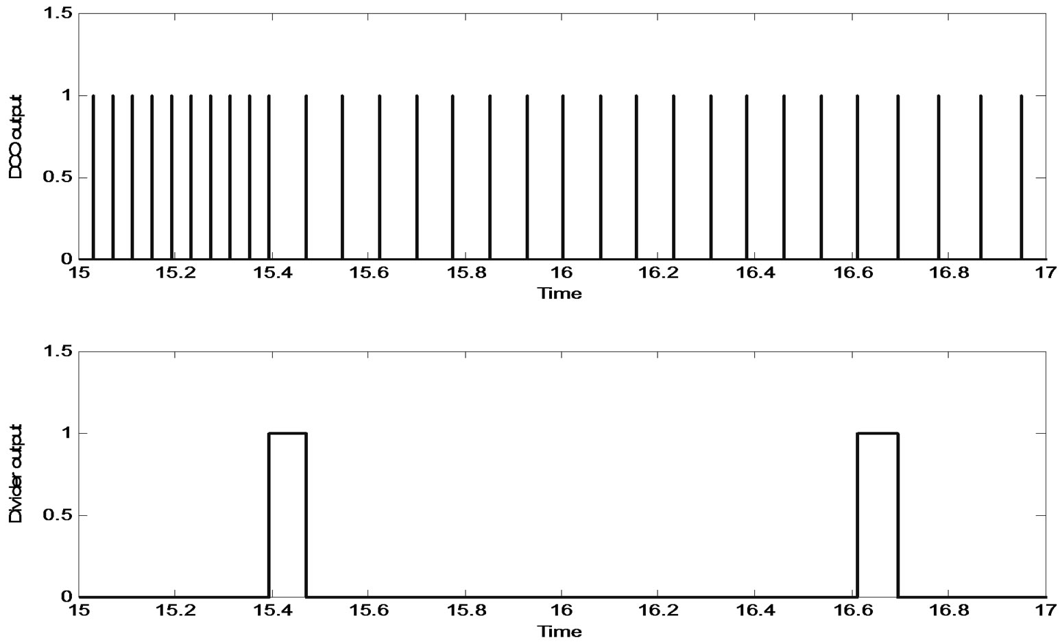
Figure 14. First-order (Top) DCO output, (bottom) Divider output for ÷16.
The achievement of locking following a system disturbance within an acceptable number of samples re-enforces the robustness aspect.
In order for the TDTL-FS system to be stable and hence usable an adaptive stabilization mechanism was incorporated with the synthesizer. The adaptive frequency sensing mechanism stabilizes the loop by controlling the gain block and the DCO of the loop in a way that counter acts the effect of the division process and brings the loop to its optimum operating point within the locking region.
The TDTL-based frequency synthesizer offers a number of advantages compared to other PLL synthesizers. These include an all digital architecture that is independent of the input signal level and a wider range of frequency synthesis. This is also coupled with relatively
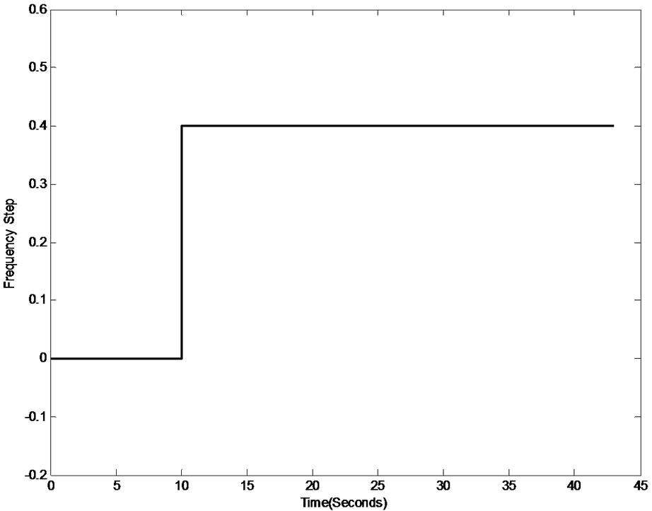
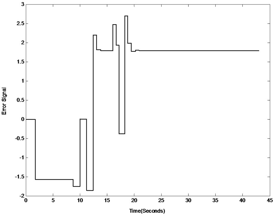
Figure 15. TDTL-FS with FSB system response to a positive frequency step (Top): Frequency step input (Bottom): Output of the phase error detector.
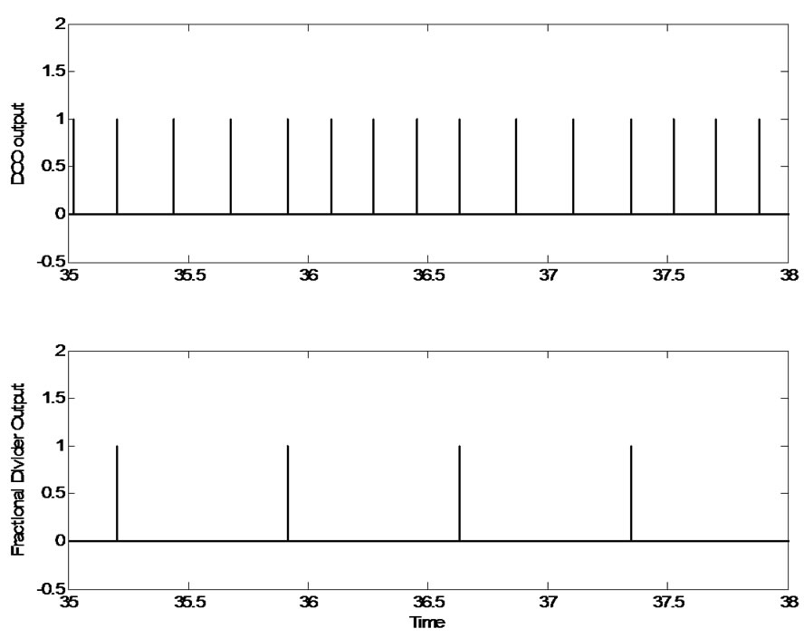
Figure 16. Output of the divider and the DCO for a division of 3.25 (Top): DCO output (Bottom): Divider output.
low system implementation complexity. The ability of the TDTL-FS to achieve locking as well as integer and fractional divisions were illustrated. The results indicate that fine divisions can be achieved. However, the speed of the adaptation process for fine divisions will need to be improved. This will be the subject of further work in the future.
6. References
[1] Y. Kim, B. Jang Jeong, J. Chung, C. Hwang, J. S. Ryu, K. Kim, and Y. Kim, “Beyond 3G: Vision, requirements, and enabling technologies,” IEEE Communications Magazine, Vol. 41, No. 3, pp. 120-124, March 2003.
[2] A. Goldsmith, “Wireless communications,” Cambridge University Press, 2005.
[3] P. Liu, Z. Tao, Z. Lin, E. Erkip, and S. Panwar, “Cooperative wireless communications: A cross-layer approach,” IEEE Wireless Communications, pp. 84-92, August 2006.
[4] C. Lam and B. Razavi, “A 2.6-GHz/5.2-GHz frequency synthesizer in 0.4-µm CMOS technology,” IEEE Journal of Solid-State Circuits, Vol. 35, No. 5, pp. 788-794, May 2000.
[5] F. M. Gardner, “Phaselock techniques,” 3rd Edition, Wiley, 2005.
[6] T. H. Lin, W. J. Kaiser, and G. J. Pottie, “Integrated low-power communication system design for wireless networks,” IEEE Communications Magazine, pp. 142-150, December 2004.
[7] R. B. Staszewski and P. T. Balsara, “All-digital frequency synthesizer in deep-submicron CMOS,” Wiley, 2006.
[8] S. T. Moon, A. Valero-Lopez, and E. Sanchez-Sinencio, “Fully integrated frequency synthesizers: A tutorial,” International Journal of High Speed Electronics and Systems, Vol. 15, No. 2, pp. 353-375, June 2005.
[9] J. Vankka and K. A. I. Halonen, “Direct digital synthesizers: Theory, design and applications,” Springer, 2001.
[10] D. D. Caro and A. G. M. Strollo, “High-performance direct digital frequency synthesizer using piecewisepolynomial approximation,” IEEE Transaction Circuits and Systems I, Vol. 52, No. 2, pp. 324-337, February 2005.
[11] M. Kozak and E. G. Friedman, “Design and simulation of fractional-N PLL frequency synthesizer,” International Symposium on Circuits and Systems, pp. 780-783, 2004.
[12] K. Shu and E. S. Sinencio, “CMOS PLL synthesizers: Analysis and design,” Springer, 2005.
[13] K. Woo, Y. Liu, E. Nam, and D. Ham, “Fast-lock hybrid PLL combining fractional-N and integer-N modes of differing bandwidths,” IEEE Journal of Solid-State Circuits, Vol. 43, No. 2, pp. 379-389, February 2008.
[14] Z. Hussain, B. Boashash, M. H. Ali, and S. A. Araji “A time-delay digital tanlock loop,” IEEE Transaction Signal Processing, Vol. 49, No. 8, pp. 1808-1815, 2001.
[15] C. Lee and C. K. Un, “Performance analysis of digital tanlock loop,” IEEE Transaction Communications, Vol. 30, pp. 2398-2411, October 1982.
[16] Z. M. Hussain, “Performance analysis of time-delay phase-shifter in additive Gaussian noise: A statistical comparison with Hilbert transformer,” 6th International Symposium on Signal Processing and Its Applications (ISSPA), August 2001.
[17] M. A. Qutayri, S. A. Araji, and N. A. Moosa, “Improved first-order time-delay tanlock loop architectures,” IEEE Transaction Circuits and Systems Part-I, Vol. 53, No. 9, pp. 1896-1908, 2006.
[18] S. R. A. Araji, Z. M. Hussain, and M. A. A. Qutayri, “Digital phase lock loops: Architectures and applications,” Springer, 2006.
[19] J. C. Osborne, “Stability analysis of an nth power digital phase-locked loop-part I: First-order DPLL,” IEEE Transaction Communications, Vol. 28, pp. 1343-1354, August 1980.
[20] Q. Nasir, “Extended lock range zero-crossing digital phase-locked loop with time delay,” EURASIP Journal on Wireless Communications and Networks, Vol. 5, No. 3, pp. 413-418, 2005.
[21] Z. M. Hussain, “Convergence behavior of first-order time-delay digital tanlock loop,” IEEE Communication Letters, Vol. 6, No. 7, pp. 291-293, July 2002.