Journal of Electromagnetic Analysis and Applications
Vol. 3 No. 4 (2011) , Article ID: 4619 , 4 pages DOI:10.4236/jemaa.2011.34018
Compact Low Pass Filter Design for L-Band Application
![]()
1Electronics and Communication, Maharaja Agrasen Institute of Technology, Delhi, India; 2Ambedkar Institute of Technology, Geeta Colony, Delhi, India.
Email: dhirendra_007@rediffmail.com, asok.de@gmail.com
Received January 30th, 2011; revised March 11th, 2011; accepted March 21st, 2011
Keywords: Low Pass Filter, Chebyshev Prototype, Stepped Impedance Etc
ABSTRACT
An effective technique to design compact low pass filter has been proposed in this paper. The proposed method is highly effective for L-band applications. Low impedance microstrip lines are arranged such that they work as open stubs to increase the selectivity of the filter. Using the proposed technique about 57% size reduction has been realized with sharper roll off characteristics. An empirical expression is derived to determine the dimension of resonators. For cut-off frequency of 1.7 GHz the investigated method has been fabricated and tested. There is a close agreement between simulated and measured results.
1. Introduction
The compact size and suppression of unwanted frequency components with excellent passband characteristic is the major concern of the microwave low pass filters design. To achieve the compact size printedcircuit technology is generally preferred to design the planar microwave filters. This technique also provides easy fabrication, low cost as well as easy integration with other microwave circuits. Conventional design of microstrip low pass filters basically involves either use of shunt stubs or using the stepped impedance network that is high-low impedance transmission line [1-2]. Using the above methods, a large number of inductive and capacitive elements are required to achieve shaper roll-off characteristic thus the resultant filters occupy larger area. There are several methods to reduce the size of microstrip low pass filters which have been reported [3-9]. One of the effective methods of size reduction is to introduce slow wave structure either in the main line [4-5] or on the ground plane [6-9]. In [4] a spiral resonator is used to replace the stepped impedance ladder network in the conventional design. The unsymmetrical stubs have also been used in [5] to design a compact filter. These methods increase the circuit complexity. The slow wave effect on the ground plane can be introduced by using the defective ground structures (DGS). The overall inductance and capacitance of the resonators can be increased using DGS and thus the compact circuit size can be achieved. The defects on the ground plane may cause unwanted radiation and it is difficult to integrate with other microwave components.
In this paper, a compact microstrip low pass filter has been proposed with sharper roll-off characteristics. An empirical expression has been derived to provide the direct calculation of the lengths of the resonators. The basic concept used for the proposed technique has also been discussed critically. The designed filter has been fabricated and tested.
2. Basic Theory of Proposed Design
To design passive low pass prototype filter, amplitudesquared transfer function may be used [1]. In the proposed design the insertion loss technique with Chebyshev approximation has been applied. Chebyshev approximation of a two port filter network is a mathematical description of the filter response which results equal-ripple in pass band and maximally flat stop band. In microwave filters it defines the transmission parameter S21. The Chebyshev low pass prototype filter is a ladder network with series inductors and shunt capacitors, for five poles it has been shown in Figure 1. The inductance and capacitance of various components can be calculated from the normalized values of gk (where k = 1, 2, 3, 4, 5) as given in Equations (1) and (2) respectively.
 (1)
(1)
 (2)
(2)
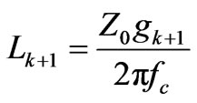
where L and C are the inductances and capacitances of the resonators. Z0 is the source and load impedances, fc is the cut-off frequency in hertz. The electrical lengths for the inductors and capacitors for microstrip structure are proportional to the respective inductances and capacitances [1].
 for inductor
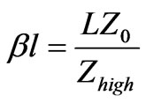
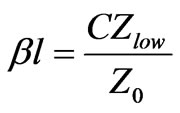 for capacitor where β is the phase constants, l is physical lengths of resonators, Zhigh and Zlow are the impedance of inductive and capacitive lines respectively.
The constant g0 and g6 shown in Figure 1 are the normalized values of source and load impedances.
3. Design Equations
To calculate the lengths of the resonators for the proposed method, the value of f(x) is determined for desired cut-off frequency x (in GHz) using Equation (3) which is a polynomial of the fourth order that has been empirically derived. This equation has been derived by using curve fitting of simulated results for different cut off frequencies. From the Equations (4) and (5) it is clear that the lengths of inductive components are inversely proportional to the corresponding impedance, whereas the lengths of capacitive elements are proportional to the corresponding impedances. Since as the cut-off frequency decreases the length of the resonators increases. This makes the length of resonators for L-band application so large. The value of f(x) has been used to calculate the lengths of inductive and capacitive lines by using the Equations (4) and (5) respectively. The layout of the filter is shown in Figure 2. From this figure it can be visualized that this structure is high-low impedance ladder
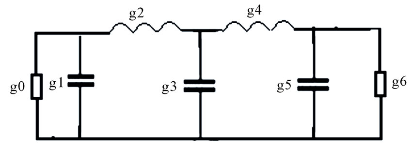
Figure 1. Low pass prototype network with five components.
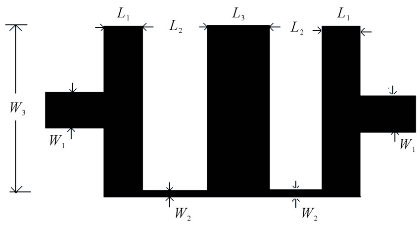
Figure 2. Lay out of the proposed design.
network in which the high impedance lines are placed at one end of the low impedance stubs. It has been studied that as the position of high impedance line shifted towards the end from the central position the values of overall capacitance increases and hence the cut-off frequency reduces.
 (3)
(3)
 (4)
(4)
 (5)
(5)
where  and
and ![]() are the physical lengths and
are the physical lengths and  and
and  effective dielectric constant of inductive (smaller width) and capacitive lines (wider width).
4. Result and Discussion
For the proposed design, a fifth order Chebyshev response for 0.1 dB ripple has been considered. The cut off frequency is considered as 1.7 GHz. The presented filter has been fabricated using the substrate FR4 with dielectric constant 4.5 and height 1.5 mm. By using the design equations given in the previous section the lengths of the inductive and capacitive line sections have been calculated for the frequency x = 1.7 GHz. The dimensions are calculated as length of low impedance resonators L1 = 1.41 mm, length of central stub is L3 = 2.44 mm, lengths of the inductive lines are L2 = 2.64 mm width of inductive lines are W2 = 0.1 mm and width of the capacitive lines are W3 = 20 mm and the width of the 50 ohm line is W1 = 2.81 mm. The designed structure is simulated using MoM based full wave electromagnetic simulation software IE3D [9] and fabricated using photolithographic technique. The fabricated structure is shown in Figure 3. There is a good agreement between the simulated and measured results. The measured and simulated S11 and S21 parameters are shown in the Figures 4 and 5 respectively. In the pass band the maximum return loss in 22.9 dB. The
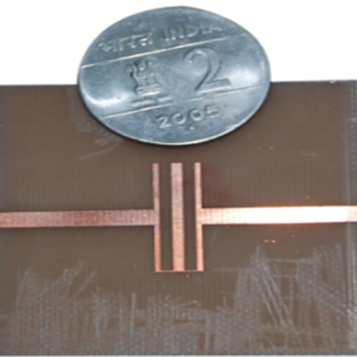
Figure 3. Fabricated structure of the proposed LPF.
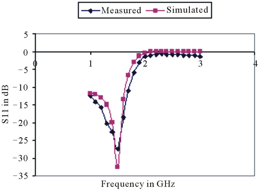
Figure 4. Measured and Simulated S11 parameter of designed structure.
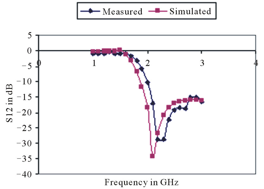
Figure 5. Measured and Simulated S21 parameter.
insertion loss reaches more than 25 dB at about 2.2 GHz.
5. Conclusion
In this work a simple design method has been proposed to design a compact low pass filter. The size of the proposed design occupies 2.34 times lesser area than the conventionally designed low pass filters. That is using the proposed technique about 57% size reduction has been realized. This filter shows more than 22 dB insertion loss within 0.5 GHz.
REFERENCES
- D. M. Pozar, “Microwave Engineering,” Wiley, 2007.
- J. S. Hong, M. J. Lancaster, “Microstrip Filters for RF/ Microwave Applications,” John Wiley & Sons, Hoboken, 2001. doi:10.1002/0471221619
- I. S. Kim and S. W. Yun, “Compact LPF Using Asymmetrical Microstrip Step Discontinuity for Harmonic Suppression,” Electronics Letters, Vol. 41, No. 16, 2005, pp. 41-42.
- J. Gu and X. Sun, “Compact Lowpass Filter Using Spiral Compact Microstrip Resonant Cells,” Electronics Letters, Vol. 41, No. 19, 2005, pp. 1065-1066.
- K. Deng, Q. Xue and W. Che, “Improved Compact Microstrip Resonance Cell Lowpass Filter with Wide Stopband Characteristics,” Electronics Letters, Vol. 43, No. 8, 2007, pp. 463-464. doi:10.1049/el:20070028
- D. Ahn, J. S. Park, C. S. Kim, J. Kim, Y. Qian and T. Itoh, “A Design of Lowpass Filter Using the Novel Microstrip Defected Ground Structure,” IEEE Transactions on Microwave Theory and Techniques, Vol. 49, No. 1, January 2001, pp. 86-93. doi:10.1109/22.899965
- J. S. Lim, C. S. Kim, D. Ahn, Y. C. Jeong and S. Nam, “Design of Low Pass Filter Using Defected Ground”, IEEE Transactions on Microwave Theory and Techniques, Vol. 53, No. 8, August 2005, pp. 2539-2545.
- J. P. Yang and W. Wu, “Compact Elliptical Low-Pass Filter Using Defected Ground Structure,” Microwave and Wireless Components Letters, Vol. 18, No. 9, September 2008, pp. 578-580.
- IE3D User’s Manual, Zeland Software, Inc., December 1999.