Materials Sciences and Applications
Vol.4 No.4(2013), Article ID:30565,6 pages DOI:10.4236/msa.2013.44027
Optimized Distribution and Morphology of Carbon Nanofibers for a Field Emitter Grown by Nickel and Chromium Cosputtering
![]()
1Graduate School of Environmental Studies, Tohoku University of Aoba, Sendai, Japan; 2Institute of Multidisciplinary Research for Advanced Materials, Tohoku University Katahira, Sendai, Japan.
Email: *shimoi@mail.kankyo.tohoku.ac.jp
Copyright © 2013 Norihiro Shimoi, Shun-Ichiro Tanaka. This is an open access article distributed under the Creative Commons Attribution License, which permits unrestricted use, distribution, and reproduction in any medium, provided the original work is properly cited.
Received January 28th, 2013; revised February 26th, 2013; accepted March 29th, 2013
Keywords: Alloys; Carbon Fibres; Metal-Matrix Composites; X-Ray Diffraction; Chemical Vapour Deposition (CVD)
ABSTRACT
To obtain a high field emission (FE) current with a low driving voltage, it is important to control and optimize carbon nanofiber (CNF) array patterns for FE. While there have been various means for controlling CNF array patterns reported over the past few decades, array patterning using lithography is the method typically used to control CNF morphology. Because lithography uses many masks and is costly, it is necessary to establish a simpler process. In this study, the grain size and distribution of catalysts with phase separation were controlled. A system which controls the morphology of small bundles of CNFs was constructed with the distance between the bundles kept constant in order to obtain a higher FE current. The Ni catalyst layer for forming the CNF morphology was separated by noncatalytic Cr grains formed by cosputtering. As a result, it was possible to control the Ni content, the grain size and synthesis density of CNFs in the alloy with a varying number of nickel pellets placed on the chromium target. This method is an epochmaking CNF patterning technique very different from lithography.
1. Introduction
Since the principle of the electron emission mechanism using a field emission (FE) phenomenon was proposed in 1928 by Fowler and Nordheim [1], the results of the mechanism and application development for FE have been reported extensively. One example is the design for obtaining electron emission effectively and research on materials for FE. The first time the results of applied research into the practical applications of a field emission device, however, were reported was in 1976 by Spindt et al. [2]. The electron source they used was an FE cathode made of molybdenum (Mo) and tungsten (W), which, due to their high melting points, can withstand relatively high temperatures, and therefore, the FE cathode was capable of intensively emitting electrons from its tip. The research and development on the application of FE electron sources has been extensively reported since 1976.
In the FE source mentioned above, the metal FE emitter had to be pointed, because it is necessary to yield high electric field strength of about 107 V/cm at the tip. At a high vacuum of more than 10−5 Pa, the degradation of electron emission by the contamination of the metal surface is prevented.
The applicability of carbon nanorods as an FE source has been studied since the discovery of carbon nanofibers (CNFs) which coexist with carbon nanotubes (CNTs) and CNFs can be synthesized on catalysts [3-5]. In this work, we used carbon nanofibers (CNFs) which were grown uniformly on a glass substrate industrially using a low temperature process as the FE emitters. CNFs have a higher work function than metals [6] and are rod-shaped, which provides tips for the concentration of electric fields. Focusing on this feature, de Heer et al. confirmed FE electron emission from CNFs in 1995 [7].
There are two types of parameters for evaluating FE (FE parameter): one is the field enhancement factor, which represents the concentration of the electric field; and the other is the electron emission site, which is the area for emitting electrons. To improve these parameters, it is necessary to optimize the form of the emitter so that a high current at a low driving voltage can be obtained. In this study, the authors examined the CNF control of an array of FE characteristics.
A CNF array of controlled impact on FE characteristics was first reported in 2000 by Nilsson et al., obtained without optimizing the crystalline form. They patterned the array on catalyst layers to synthesize CNFs. When the distance between adjacent patterns of synthesizing CNFs is at least twice the CNF length, they found that the field strength focused on those CNFs was almost the same as a CNF standing alone. There are many reports on the optimization of FE properties with CNF array patterning that followed the reports of Nilsson et al. [8-24]. In some these reports, the patterning of CNFs by lithography, which commonly uses semiconductor process technology, was explained. We examined the surface morphology to optimize the FE parameters, namely, the field enhancement factor and electron emission site.
Our idea for obtaining high FE current with low power consumption by controlling the CNF synthesis morphology is shown in Figure 1. When a CNF stands on the substrate, as in Figure 1, the electric field is concentrated at the tip of the CNF because there are no obstacles to the penetration of potential lines. When the electron emission sites are limited to an area with only one CNF, it is impossible to achieve a high emission current. On the other hand, when many CNFs stand on the substrate, as in Figure 1, the space between adjacent CNFs is so narrow that it is difficult for the equipotential lines to penetrate it. As a consequence, the electric field on top of each CNF is smaller than just one CNF standing alone. However, when many CNFs exist as emissions sources, the CNF emission site is larger than just one CNF. From these ideas, when CNFs are arranged in bundles, and when the size and space between these CNF bundles is controlled, the authors surmised that it is possible to optimize both the field enhancement factor and the electron emission site.
To improve FE properties, there have been many studies in which the spacing between CNFs was discussed. Since Nilsson et al. reported the relationship between array patterning and the electric field on the top of the CNF, many studies into the control of CNF surface morphology using lithography with semiconductor process technology have been conducted. The process is complex and the cost of establishing a CNF array is high. It is thus necessary to apply a FE emitter as an industrial device to simplify the process for FE emitters with CNFs and to limit the cost of the process. Therefore, in this study, the authors plan to establish a simpler CNF array pattern control method.
2. Experiment of CNF Array Pattern Control
In this study, CNF array pattern control with catalysts and other materials by the phase separation of grains was attempted. CNF catalyst layers were separated by a separator material, and CNFs were synthesized only on the catalyst layer. Then the catalyst grains were separated at submicron sizes using a noncatalyst metal. In the formation of a catalyst microstructure separated by a noncatalyst, a eutectic alloy allows for phase separation with grains of the catalyst layer controlling of contents of catalyst and noncatalyst. Nickel (Ni) was used as a catalyst to synthesize stable CNFs [22-27] which form catalyst patterns with small grains at low temperature. Chromium (Cr), which is used as the electrode in flat panel displays and is known for its excellent rigidity and durability, was used as the nonmetal catalyst for the separation of Ni grains.
The sputtering deposition method was adopted to fabricate a Ni-Cr alloy film on a large area of the electrode. A schematic diagram of the sputtering setup is shown in Figure 2. A SH550 manufactured by ULVAC was used in this study.
3. Results and Discussion
3.1. Formation of Ni-Cr Alloy by Cosputtering
As shown in Figure 2, Ni pellets of 99.9% purity were
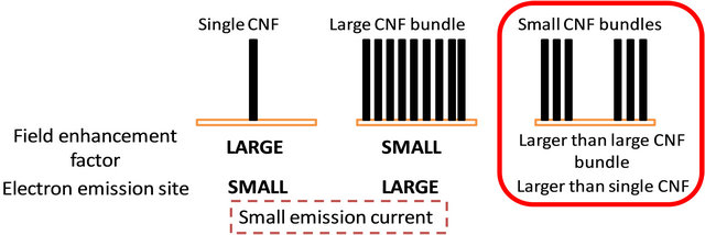
Figure 1. Idea for increasing the FE parameters by controlling the CNF morphology. Small CNF bundles provide a larger field enhancement factor and field emission site.

Figure 2. Schematic of the Ni and Cr cosputtering method.
placed on Cr targets, and a Ni-Cr alloy film was formed by cosputtering both Ni and Cr. The composition of the alloy was controlled by adjusting the number of Ni pellets on the Cr target. The conditions for cosputtering deposition are given in Table 1.
The photograph in Figure 3 shows the morphology of the Ni-Cr alloy deposited by cosputtering. From the analysis with SEM-EDS (device name: SEM: S-3500NLC (Hitachi Science Systems), EDS: EDAX GENESIS), it was found that lamellar grains consist of Ni, whereas other components consist of Cr layers. The SEM images of the morphology of the alloy with Ni contents of 37, 57 and 86 wt% according to both condition of 734 K and 373 K at the temperature of substrate on co-sputtering are shown in Figure 3. Figure 3(a) shows SEM images of the morphologies of the alloy at 734 K on a substrate by cosputtering, and Figure 3(b) shows the SEM images at 373 K on a low substrate temperature. The Cr grains in Figure 3(a) aggregated as fine grains at high temperature, with Ni grains ~1 μm in size aggregating in a lamellar pattern. The Ni contents is 57 wt% at the high temperature, and the size of the grains was shown to be dependent on the number of Ni pellets placed on the Cr target. The morphology of the Ni-Cr alloy in Figure 3(b) formed at low temperature by cosputtering did not have clearly divided Ni and Cr domains. Notably, no Ni grains were detected in the synthesis of CNFs with Ni contents of 37 wt%. The Ni-Cr alloy has a eutectic phase, and a mixed crystal with an amorphous composition of Ni and Cr is formed at low substrate temperatures by cosputtering. This explains why no clear boundary was constructed between the Ni and Cr crystals.
Figure 4 shows a plot of Ni content vs the number of Ni pellets on the Cr target. The Ni content was determined by averaging according to the by SEM-EDS images of the cosputtered samples. The Ni content in the Ni-Cr alloy was proportional to the number of Ni pellets on the Cr target, and did not depend on the temperature of the substrate when cosputtering. As such, it was surmised that Ni content can be controlled by adjusting the number of Ni pellets used in cosputtering. The synthesis morphology of Ni-Cr, however, was confirmed to differ according to the substrate temperature when cosputtering.
Table 1. Cosputtering conditions with Ni and Cr targets.

(a)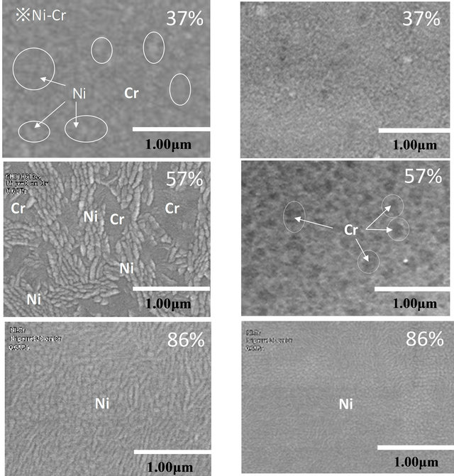 (b)
(b)
Figure 3. SEM images of the Ni-Cr morphology of alloys with various Ni contents and its dependence on substrate temperature during the cosputtering process. (a) 743 K at substrate temperature in cosputtering; (b) 373 K at substrate temperature in cosputtering.
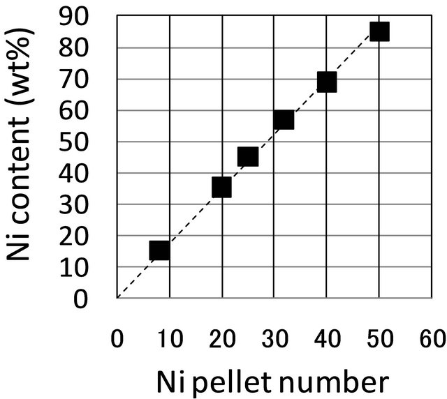
Figure 4. Relationship between the Ni pellet number on Cr target and Ni content by cosputtering at 743 K as evaluated by EDS. At 373 K, the results show the same tendency.
3.2. Control of CNF Growth Morphology
After cosputtering with Ni and Cr, CNFs on the samples were synthesized by plasma-enhanced chemical vapor deposition (PECVD). This synthesis method is capable of growing a large number of CNFs, and the number is proportional to the size of the reactor of the CVD. The advantage of this method is that CNFs can be controllably grown on Ni catalyst grains perpendicular to the substrate.
A helicon-wave-assisted PECVD was used to induce CNF growth at a low temperature [28]. CNFs synthesized by this method stand in bundles and have been characterized as arrayed with space between adjacent bundles. Figure 5 shows the CNF synthesis morphology with a Ni alloy catalyst with a Ni content formed at high temperature (743 K) by cosputtering. CNFs were synthesized uniformly with a diameter of about 100 nm f and a length of 1 μm regardless of the Ni formation. A crosssectional view of the synthesized CNFs in Figure 5(b) is shown in Figure 6: the high concentration of Ni catalysts at the top indicates that CNFs grew on the Ni catalyst in the Ni-Cr alloy. The cross-sectional view of CNFs obtained by TEM, shown in Figure 6(b), resembles the cup-stacked structure of graphene. CNFs with a Ni catalyst at the top were predominantly synthesized from {111} of the Ni plane orientation [29].
As determined from the surface morphology of the CNFs on Ni-Cr alloy catalysts shown in Figure 5, the number of CNFs per unit area vs Ni content is plotted in Figure 7. The triangles indicate the number of CNFs at high growth temperature by cosputtering, and the circles are the datum from the low growth temperature of Ni-Cr catalyst. The results indicate that the control of CNF synthesis was possible by controlling the Ni content in the Ni-Cr catalyst. Moreover, the density of CNFs on the Ni-Cr catalyst was dependent on the substrate growth temperature by cosputtering, and the CNFs had poor density on the Ni-Cr catalyst grown at low temperature. It should be noted that no CNFs were synthesized on the Ni-Cr catalyst at 37 wt% Ni content at low temperature growth.
The results of the X-ray diffraction measurements, which indicate the dependence of growth temperature on the Ni-Cr catalyst, are shown in Figure 8. At low growth temperature, clear Ni-Cr alloy peaks were observed. The diffraction peaks of Ni appear as the Ni content increases. This means polycrystalline Ni grains are formed for the synthesizing of CNFs instead of the Ni-Cr alloy. The amount of Ni in the Ni-Cr catalyst is directly correlated with the density of CNF synthesis, as shown in Figure 7. It would appear that a Ni-Cr crystal alloy including amorphous Ni and Cr can be grown at low temperature, and this Ni-Cr alloy impedes the growth of CNFs in the plasma atmosphere of the PECVD. It is necessary to increase the number of Ni grains in Ni-Cr alloy for the synthesis of CNFs.
From this morphology, the FE properties that indicate the field enhancement factor and the electron emission site were found to be controllable by adjusting the Ni content and the crystalline phase, and it was possible to obtain FE current with low power consumption [30].
4. Conclusion
It was shown to be possible to control the CNF synthesis morphology selectively on a Ni-Cr alloy catalyst. A Ni catalyst layer was formed by cosputtering with Ni and Cr, and the Ni catalyst for CNF growth was separated from the Cr grain by phase separation. By using this alloy as the catalyst, CNFs were successfully synthesized only on the Ni catalyst and the synthesis density of the CNFs was found to be dependent of the Ni content of the Ni-Cr alloy catalyst. As a result, the array of CNF patterning was able to be controlled without lithography.

Figure 5. SEM images of CNF bundles grown on Ni-Cr and pure nickel catalyst films at 743 K temperature growth. The Ni concentration of the Ni-Cr catalyst layer was larger in (b) than in (a). Uniformly distributed CNFs were obtained on almost pure Ni (c) with a density of more than 50 fibers per μm2; they were longer than those grown on a Ni-Cr catalyst [28].
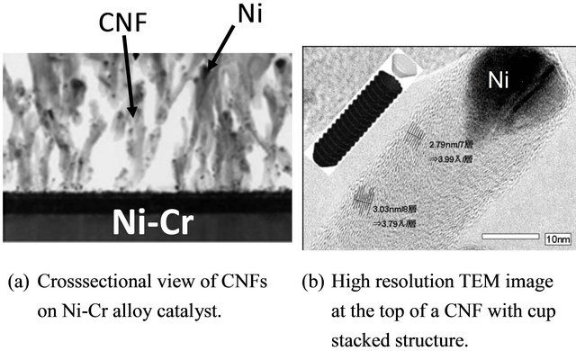
Figure 6. TEM images of synthesized CNFs on a Ni-Cr alloy catalyst.
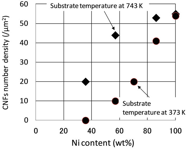
Figure 7. Relationship of number density of CNFs on Ni content in the Ni-Cr alloy catalyst against the dependence of growth temperature of the Ni-Cr catalyst.

Figure 8. The X-ray diffraction measurements indicating their dependence on the growth temperature of the Ni-Cr catalyst. The PDF number of each XRD curves is CrPDF#06-0694/Ni-PDF#04-0850/NiCr-PDF#26-0429.
5. Acknowledgements
This work was partially supported by the Global COE Program “Materials Integration International Center of Education and Research, Tohoku University,” MEXT, Japan.
REFERENCES
- R. H. Fowler and L. W. Nordheim, “Electron Emission in Intense Electric Fields,” Proceedings of the Royal Society A, Vol. 119, No. 781, 1928, pp. 173-181. doi:10.1098/rspa.1928.0091
- C. A. Spindt, I. Brodie, L. Humphery and E. R. Westerberg, “Physical Properties of Thin-Film Field Emission Cathodes with Molybdenum Cones,” Journal of Applied Physics, Vol. 47, No. 12, 1976, pp. 5248-5263. doi:10.1063/1.322600
- K. H. Park, J. H. Yim, S. Lee and K. H. Koh, “Catalyst-Assisted Hot Filament Chemical Vapor Deposition and Characterization of Carbon Nanostructures,” Thin Solid Films, Vol. 501, No. 1-2, 2006, pp. 233-237. doi:10.1016/j.tsf.2005.07.160
- I. Willems, Z. Kónya, J.-F. Colomer, G. Van Tendeloo, N. Nagaraju, A. Fonseca and J. B. Nagy, “Control of the Outer Diameter of Thin Carbon Nanotubes Synthesized by Catalytic Decomposition of Hydrocarbons,” Chemical Physics Letters, Vol. 317, No. 1-2, 2000, pp. 71-76. doi:10.1016/S0009-2614(99)01300-7
- S. L. Sung, S. H. Tsai, C. H. Tseng, F. K. Chiang, X. W. Liu and H. C. Shih, “Well-Aligned Carbon Nitride Nanotubes Synthesized in Anodic Alumina by Electron Cyclotron Resonance Chemical Vapor Deposition,” Applied Physics Letters, Vol. 74, No. 2, 1999, pp. 197-199. doi:10.1063/1.123291
- A. Di Bartolomeo, A. Scarfato, F. Giubileo, F. Bobba, M. Biasiucci, A. M. Cucolo, S. Santucci and M. Passacantando, “A Local Field Emission Study of Partially Aligned Carbon-Nanotubes by Atomic Force Microscope Probe,” Carbon, Vol. 45, No. 15, 2007, pp. 2957-2971. doi:10.1016/j.carbon.2007.09.049
- W. A. de Heer, A. Chatelain and D. Ugarte, “A Carbon Nanotube Field-Emission Electron Source,” Science, Vol. 270, No. 5239, 1995, pp. 1179-1180. doi:10.1126/science.270.5239.1179
- W. B. Choi, D. S. Chung, S. H. Park and J. M. Kim, “A 4.5-in Fully Sealed Carbon Nanotube-Based Field-Emission Flat-Panel Display,” SID Symposium Digest of Technical Papers, Vol. 30, No. 1, 1999, pp. 1134- 1137.
- L. Nilsson, O. Groening, C. Emmenegger, O. Kuettel, E. Schaller and L. Schlapbach, “Scanning Field Emission from Patterned Carbon Nanotube Films,” Applied Physics Letters, Vol. 76, No. 15, 2000, pp. 2071-2073. doi:10.1063/1.126258
- Z. Yuning, L. Wei, Z. Xiaobing, and W. Baoping, “Calculation of the Emission Performance of the Carbon Nanotube Array,” Applied Surface Science, Vol. 245, No. 1-4, 2005, pp. 400-406. doi:10.1016/j.apsusc.2004.10.042
- Y.-H. Wu, C.-M. Hsu, C.-T. Chia, I.-N. Lin and C.-L. Cheng, “Field Emission and Raman Spectroscopy Studies of Atomic Hydrogen Etching on Boron and Nitrogen Doped DLC Films,” Diamond and Related Materials, Vol. 11, No. 3, 2002, pp. 804-808. doi:10.1016/S0925-9635(01)00696-3
- L. Xinghui, Z. Changchun and L. Yukui, “Energy Band Structure Effect of Individual Single-Walled Carbon Nanotubes on Field Emission Characteristics,” Physica B: Condensed Matter, Vol. 344, No. 1-4, 2004, pp. 243-248. doi:10.1016/j.physb.2003.09.265
- Y. J. Jung, G. H. Son, J. H. Park, Y. W. Kim, A. S. Berdinsky, J.-B. Yoo and C.-Y. Park, “Fabrication and Properties of Under-Gated Triode with CNT Emitter for Flat Lamp,” Diamond and Related Materials, Vol. 14, No. 11-12, 2005, pp. 2109-2112. doi:10.1016/j.diamond.2005.07.029
- J.-H. Han, T. Y. Lee, D. Y. Kim, J.-B. Yoo, C.-Y. Park, J. J. Choi, T. Jung, I. T. Han and J. M. Kim, “Field Emission Properties of Carbon Nanotubes Grown on Co/TiN Coated Ta Substrate for Cathode in Microwave Power Amplifier,” Diamond and Related Materials, Vol. 13, No. 4-8, 2004, pp. 987-993. doi:10.1016/j.diamond.2003.11.014
- D. Kim, S. H. Lim, A. J. Guilley, C. S. Cojocaru, J. E. Bourée, L. Vila, J. H. Ryu, K. C. Park and J. Jang, “Growth of Vertically Aligned Arrays of Carbon Nanotubes for High Field Emission,” Thin Solid Films, Vol. 516, No. 5, 2008, pp. 706-709. doi:10.1016/j.tsf.2007.06.089
- X. Q. Wang, M. Wang, H. L. Ge, Q. Chen and Y. B. Xu, “Modeling and Simulation for the Field Emission of Carbon Nanotubes Array,” Physica E, Vol. 30, No. 1-2, 2005, pp. 101-106. doi:10.1016/j.physe.2005.07.012
- Y. Li and H.-W. Cheng, “Numerical Simulation of Field Emission Efficiency of Anodic Aluminum Oxide Carbon Nanotube Field Emitter in the Triode Structure,” Computer Physics Communications, Vol. 179, No. 1-3, 2008, pp. 107-111. doi:10.1016/j.cpc.2008.01.026
- W. Liu, C. Zhu, C. Meng and F. Zeng, “On the Uniformity of Field Emission in Screen Printed CNT-Cathodes: The Effects of the Cathode Roughness,” Microelectronics Journal, Vol. 37, No. 5, 2006, pp. 404-408. doi:10.1016/j.mejo.2005.06.004
- T. Matsuda, M. Mesko, A. Ogino and M. Nagatsu, “Synthesis of Vertically Aligned Carbon Nanotubes on Submicron-Sized Dot-Catalyst Array Using Plasma CVD Method,” Diamond and Related Materials, Vol. 17, No. 4-5, 2008, pp. 772-775. doi:10.1016/j.diamond.2007.08.030
- S. H. Jeong and K. H. Lee, “Fabrication of the Aligned and Patterned Carbon Nanotube Field Emitters Using the Anodic Aluminum Oxide Nano-Template on a Si Wafer,” Synthetic Metals, Vol. 139, No. 2, 2003, pp. 385-390. doi:10.1016/S0379-6779(03)00187-5
- M. A. Guillorn, M. L. Simpson G. J. Bordonaro, V. I. Merkulov, L. R. Baylor and D. H. Lowndes, “Fabrication of Gated Cathode Structures Using an in situ Grown Vertically Aligned Carbon Nanofiber as a Field Emission Element,” Journal of Vacuum Science and Technology B, Vol. 19, No. 2, 2001, pp. 573-578. doi:10.1116/1.1358855
- J. Erlebacher, M. J. Aziz, E. Chason, M. B. Sinclair and J. A. Floro, “Spontaneous Pattern Formation on Ion Bombarded Si(001),” Physical Review Letters, Vol. 82, No. 11, 1999, pp. 2330-2333. doi:10.1103/PhysRevLett.82.2330
- A. L. Wang, C. Neff, E. Graugnard, Y. Ding, J. S. King, L. A. Pranger, R. Tannenbaum, Z. L. Wang and C. J. Summers, “Photonic Crystals Fabricated Using Patterned Nanorod Arrays,” Advanced Materials, Vol. 17, No. 17, 2005, pp. 2103-2106. doi:10.1002/adma.200500546
- P. Chen, H.-B. Zhang, G.-D. Lin, Q. Hong and K. R. Tsai, “Growth of Carbon Nanotubes by Catalytic Decomposition of CH4 or CO on a Ni-MgO Catalyst,” Carbon, Vol. 35, No. 10-11, 1997, pp. 1495-1501. doi:10.1016/S0008-6223(97)00100-0
- W. B. Choi, Y. W. Jin, H. Y. Kim, S. J. Lee, M. J. Yun, J. H. Kang, Y. S. Choi, N. S. Park, N. S. Lee and J. M. Kim, “Electrophoresis Deposition of Carbon Nanotubes for Triode-Type Field Emission Display,” Applied Physics Letters, Vol. 78, No. 11, 2001, pp. 1547-1549. doi:10.1063/1.1349870
- M. Tanemura, T. Okita, J. Tanaka, M. Kitazawa, K. Itoh, L. Miao, S. Tanemura, S. P. Lau, H. Yang and L. Huang, “Room-Temperature Growth and Applications of Carbon Nanofibers: A Review,” IEEE Transactions on Nanotechnology, Vol. 5, No. 5, 2006, pp. 587-594. doi:10.1109/TNANO.2006.880428
- N. Sano, M. Naito and T. Kikuchi, “Enhanced Field Emission Properties of Films Consisting of Fe-Core Carbon Nanotubes Prepared under Magnetic Field,” Carbon, Vol. 45, No. 1, 2007, pp. 78-82. doi:10.1016/j.carbon.2006.08.003
- N. Shimoi and S.-I. Tanaka, “Enhancement of Electron Field Emission from Carbon Nanofiber Bundles Separately Grown on Ni Catalyst in Ni-Cr Alloy,” Carbon, Vol. 47, No. 5, 2009, pp. 1258-1263. doi:10.1016/j.carbon.2008.12.050
- Z. B. He, C. S. Lee, J.-L. Maurice, D. Pribat, P. HaghiAshtiani and C. S. Cojocaru, “Vertically Oriented Nickel Nanorod/Carbon Nanofiber Core/Shell Structures Synthesized by Plasma-Enhanced Chemical Vapor Deposition, Carbon, Vol. 49, No. 14, 2011, pp. 4710-4718. doi:10.1016/j.carbon.2011.06.075
- N. Shimoi and S.-I. Tanaka, “Numerically Optimized Bundle Size and Distribution of Carbon Nanofibers for a Field Emitter,” Carbon, Vol. 48, No. 3, 2010, pp. 905- 911. doi:10.1016/j.carbon.2009.10.045
NOTES
*Corresponding author.