Circuits and Systems
Vol.06 No.10(2015), Article ID:60470,11 pages
10.4236/cs.2015.610022
Digitally Programmable Voltage Mode Universal Filters―A Minimal Realization
Devesh Singh1, Neelofer Afzal1, Dinesh Prasad1*, Richa Srivastava2, Kuldeep Panwar3
1Department of Electronics, Jamia Millia Islamia University, New Delhi, India
2Department of Electronics and Communication, NSIT, New Delhi, India
3Department of Electronics and Communication, HMRITM, New Delhi, India
Email: dsinghece@gmail.com, afzalneelofer@gmail.com, *dprasad@jmi.ac.in, richa_ec@yahoo.co.in,kuldeeppan, war.dce@gmail.com
Copyright © 2015 by authors and Scientific Research Publishing Inc.
This work is licensed under the Creative Commons Attribution International License (CC BY).
http://creativecommons.org/licenses/by/4.0/


Received 14 September 2015; accepted 19 October 2015; published 22 October 2015
ABSTRACT
Three voltage mode universal filter biquads using digitally programmable second generation current conveyor (CCII) are presented in this paper. Salient features of proposed filter configurations include the realization of all the filter functions except allpass, independently programmable filter parameters, no component matching constraint and low sensitivity figure. Component count of proposed filter configurations is proved to be minimal for offering aforementioned set of features. The workability of proposed circuit is verified by including the SPICE simulations.
Keywords:
Universal Filter, Voltage Mode, Digitally Programmable, Current Conveyor

1. Introduction
Programmable characteristic of analog block is essential in many applications. It is required to compensate for the undesired parameter variation caused by temperature and process. Although analog programming is used in number of the applications but the limitation on the allowable range of analog tuning voltage makes it inconvenient for low-voltage applications. Hence, in these applications, the digital control is more attractive [1] .
Digital programming techniques in contrast to analog programming techniques not only provide better accuracy in avoiding parameter race especially in low voltage environment [2] -[5] , but also offer additional advantages such as better noise immunity, power saving option [6] and most importantly compatibility to modern mixed mode (analog/digital) systems.
The CCII has been most promising candidate for analog signal processing/generation since its inception in 1970 [7] due to its well known advantages such as higher signal bandwidths, greater linearity, simple circuitry and low power consumption [8] . The introduction of digital control in CCII has further enhanced its functional flexibilities and versatilities [2] -[4] .
Digitally programmable universal filter (DPUF) structures are versatile and attractive from IC realization viewpoint. A systematic comparison presented in Section 5 shows that almost all the reported DPUFs have one or more than one of the following drawbacks: (1) realization of only three or lesser number of filter functions; (2) use of large number of active and/or passive elements; (3) programming of only one filter parameter or constrained programming.
Thus, the prime objective of this paper is to present DPUF configurations, which can provide all these essential features by using minimum possible numbers of active/passive components. Three voltage mode (VM) multiple input single output DPUFs are proposed in this paper. All these DPUFs realize all the five filter functions except allpass (AP) by proper selection of input variables. The proposed DPUFs offer attractive features such as (1) independently programmable filter parameters namely pole frequency (ω0) and quality factor (Q); (2) cascadability; (3) no component matching constraint; and (4) low sensitivity figure. For obtaining all these features, proposed DPUFs use three digitally programmable CCIIs (DPCCIIs), one voltage follower (VF) and five passive components including two capacitors only. This component count is proved to be minimal for any current mode (CM)/VM DPUFs, which provides all these features. Some additional important facts of proposed DPUF configurations need to be highlighted. Actually, the first two proposed configurations do not need VF but it is required to incorporate cascadability feature. All the three DPUFs use one floating capacitor, which is less attractive for integration [9] . However, new IC technologies are capable of implementing efficient floating capacitor as double poly layer capacitor [10] . Thus, this does not impose any constraint if integration of proposed filter is to be carried out.
This paper is organized as follows. Starting from the Introduction, Section 2 briefly illustrates the use of DPCCII. Section 3 presents the realization of proposed DPUF. Section 4 discusses sensitivity performance and parasitic effects. Section 5 presents the systematic comparison of proposed DPUFs. Section 6 deals with simulation result and finally, paper is concluded in Section 7.
2. Overview of DPCCII
Literature reports number of DPCC structures [2] -[4] [11] . The concept of digital control in all these structures are similar and is based on employing an n-bit current division/summing network (CDN/CSN), which scales up (amplification) or scales down (attenuation) the current gain of conventional CCII. In order to describe the functioning of proposed configurations more clearly, the DPCC of [2] is used in this paper. Transfer matrix of DPCCII is expressed as
 (1)
(1)
where K denotes the decimal equivalent of applied n-bit codeword (=an−1, an−2, ・・・, a0). It is given as
 (2)
(2)
where j denotes the jth bit of applied codeword. Parameter α (and β) denotes the non-ideal voltage (and current) transfer gains of DPCCII. Both the gain parameters α and β are ideally unity. Plus (+) and minus sign (−) in matrix (1) denotes the positive and negative DPCCII blocks respectively. Power integer m = −1 denotes current attenuation (K−1 = K− = 1/K) in range “1 to 1/(2n−1)” while m = +1 denotes current amplification (K+1 = K+ = K) in range “0 to (2n−1)”.
DPCCII in symbolic form may be represented as four port block as shown in Figure 1(a). But for simplified presentation, modified block diagram shown in Figure 1(b) is used in this paper. It shows ith DPCCII block with current gain K± and applied codeword K.
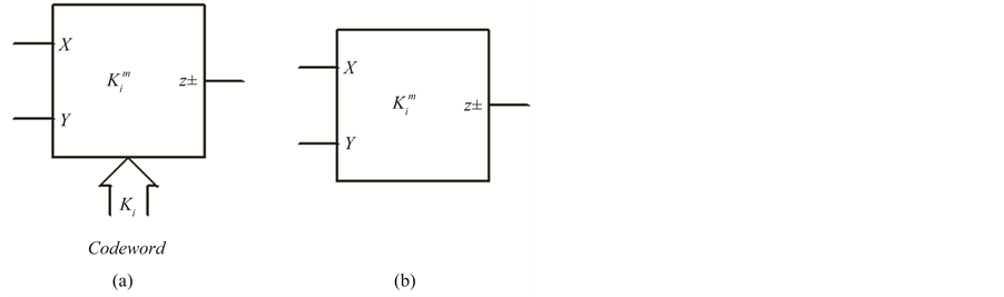
Figure 1. (a) Symbol of DPCCII; (b) Modified symbol.
3. Proposed DPUFs
This section introduces three VM second order DPUFs as depicted in Figure 2. All these configurations use three DPCCIIs, three resistors and two capacitors with additional VF required for third configuration (Figure 2(c)). Attractive features common in all the configurations are:
1. Realization of lowpass (LP), highpass (HP), bandpass (BP), band reject (BR) filter functions;
2. Independently programmable ω0 and Q;
3. No component matching constraint;
4. Cascadability with the aid of one VF in first two configurations;
5. Only single circuit configuration is used for programming all the filter functions.
The key difference of these configurations lays in the modularity of filter structure i.e. the employment of the identical active element, which simplifies circuit design of DPUF. All the configurations are different in the sense that they use different variants of DPCCII. The First DPUF (Figure 2(a)) whereas uses three variant of DPCCII namely DPCCIIK−, DPCCIIK+ and negative DPCCIIK+, the Second DPUF uses (Figure 2(b)) only two variants i.e. two DPCCIIK− and one negative DPCCIIK−. All the features of these two configurations are same. One important feature in which these two configuration lacks is the cascadability. This feature can be introduced by employing one VF. The Third configuration (Figure 2(c)) employs one VF and three blocks of DPCCIIK− type only. The VF consists of same circuitry as used between port X and Y of DPCCII (2). The Third DPUF does not need any additional follower for cascadability because it is already equipped with this feature.
Routine analysis of all the configuration yields following output function:
 (3)
(3)
It can be seen from Equation (3) and Table 1 that all the proposed DPUFs are capable of realizing four filter functions (LP, HP, BP and BR) by proper selection of input variables. It is to be noted that all the proposed DPUFs needs one inverting voltage buffer (IVB) for realizing the fifth filter function i.e. AP.
Setting codeword K2 = K3, Equation (3) reduces to
 (4)
(4)
From Equation (4), the ω0 and Q-factor can be expressed as
 (5a)
(5a)
 (a)
(a) (b)
(b) (c)
(c)
Figure 2. (a) First DPUF; (b) Second DPUF; (c) Third DPUF.

Table 1. Filter functions for various input combinations.
*Vi shows the actual applicable input. #AP needs one IVB.
 (5b)
(5b)
It can be seen from Equation (5) that ω0 and Q of all the responses are independently programmable through codeword K2(=K3) and K1 respectively. One additional advantage offered by DPUF is the programming of ω0 in either direction by simply reversing the gain parameter of respective block i.e. changing the gain K+ (or K−) of DPCCII-2, 3 by K− (or K+) or vice versa (Equation (5a)). This is particularly useful in achieving low frequency operation (for gain K−) without requiring large passive component values.
Rewriting Equation (5) for C1 = 2C2 = C and equal resistor (R) results in following set of equation
 (6a)
(6a)
 (6b)
(6b)
where, ωc and Qc are defined as component dependent factors of ω0 and Q respectively. These are given as
 (7a)
(7a)
 (7b)
(7b)
Capacitance value C1 = 2C2 may be set at design level for quality factor of value  (Q = Qc) as given by Equation (6b) for K1 = 1. It is required for maximal flat LP and HP response. High-Q values required for BP and BR responses are obtained by proper choice of codeword K1, which can be increased further by adding additional transistor arrays in corresponding DPCCII i.e. in K1 block. It is to be noted that n-transistor array can realize Q-value upto (2n−1)Qc.
4. Non-Ideal Effects
This section discusses the effect of DPCCII non-idealities over the performance of proposed DPUF. These non-idealities results from (1) small error in unity transfer gains as described by Equation (2) and (2) DPCCII parasitics.
Taking the non-ideal transfer gain into account, the output function of proposed universal filters and corresponding parameter values are given in Table 2.
Active and passive sensitivities of ω0 and Q for all the three configurations may be summarized as
 (8a)
(8a)
 (8b)
(8b)
where “x” denotes various active and passive elements i.e. αi, βi, Ki, resistances, and capacitances. It is evident from Equation (10) that the sensitivity figures are within reasonable limit.
Second set of non-idealities include DPCCII parasitics. DPCCII have high valued parasitic resistance RY (or RZ) in parallel with low valued parasitic capacitance CY (or CZ) at port Y (or Z), and a low valued series resistance RX at port X. To simplify the discussion parasitic resistances at port Y and Z are not considered as these are much greater than the external resistance of circuit.
For fair comparison, VF used in DPUF of Figure 2(c) is considered to be ideal. It can be seen from Table 2 that the number of parasitics of first DPUF (Figure 2(a)) is absorbed in external DPUF components and hence, it does not create any unwanted pole. Parasitic terms causing deviation from the ideal response of (3) and needs utmost care are denoted inside the braces “{}” (same is followed for other two DPUFs). Thus, in order to minimize the effect of parasitics, frequency of operation of first DPUF is constrained below frequency ωp, given as
Table 2. Non-ideal output equation.
 (9a)
(9a)
Similarly, the operating frequency constraint of Second and Third DPUF configurations are given by Equations (9b) and (9c) respectively. These are given as
 (9b)
(9b)
 (9c)
(9c)
It can be seen from Equations (9) that the last two DPUF configurations suffer from slightly more number of parasitic effects. However, it does not pose any problem because of small values of CY, CZ (order of few femto- farads) and RX (of order of few ohms). Thus, the proposed DPUF configurations can be easily operated over the range of few megahertz.
5. Comparison
Literature reports large number of DPUFs based on different active elements. Thus, for fair comparison, active elements used in all the DPUFs (proposed and reported) are given in terms of equivalent numbers of digitally programmable current follower (DPCF) and VF. For example, a DPCC uses two followers-one DPCF and one VF. Similarly, digitally controlled current differencing buffered amplifier (CDBA) of [12] consist of two DPCF and one VF. Comparison is based on following important features.
Criteria: (1) independently programmable filter parameters ω0 & Q; (2) cascadability; (3) number of passive components; (4) number of filter functions; (5) number of active components; (6) equivalent number of followers; (7) CM/VM or mixed mode (MM).
Comparison summary given in Table 3 shows that almost all the reported DPUFs have one or more than one of the following drawbacks: (1) realization of only three or lesser number of filter functions excluding that of [12] [13] ; (2) use of large number of active [2] [11] [13] and/or passive elements [2] [11] [13] -[15] ; (3) programming of only one parameter (pole frequency- ω0) [15] -[17] or constrained programming [2] .
It can be seen from Table 3 that the DPUFs of [2] -[4] [11] [14] [16] [18] not only realizes three or lesser number of filter functions but also they require quite large number of active and passive components. Component count [active and passive] of DPUFs of [17] [19] is lower but this is because of its current mode (CM) operation, which are known to have simplified circuit configurations. Furthermore, these DPUFs needs additional active elements either for taking the current outputs available in working impedances of filter circuit [19] or for realizing all the filter functions [19] or for introducing the cascadability feature [19] or for obtaining the programming feature of second parameters (quality factor-Q) [17] . Using two additional followers (total nine); CM DPUF of [12] realizes all the filter functions but it also requires additional circuitry for providing weighted current inputs and for the programming of second filter parameter i.e. Q factor. On the other hand, proposed DPUFs needs only one IVB for the realization of fifth filter function i.e. AP. Similarly, the VM DPUFs [3] [15] , using lesser number of active components also requires additional component either for obtaining the programmability feature of second parameter [15] or for realizing all the filter functions [3] [15] . It is to be noted that VM DPUFs listed in table belongs to the single input multi output (SIMO) topology. Thus, these DPUFs not only need quite large number of components for realizing the remaining filter functions but also get constrained by component matching requirement. For example, VM DPUFs [2] [11] [15] having three filter functions (LP, HP, BP) needs minimum four resistors and one CF for realizing remaining two filter functions (BR, AP). This also puts the component matching constraint over these filter functions (BR, AP). Obviously, the component count increases further if the filter [3] [4] have two filter functions only. Similarly, the VM DPUFs [2] [11] , already having higher
Table 3. Comparison summary of DPUFs.
Y: yes; N: no; DP: digitally programmable; FDCCII: fully differential CCII; *ω0 programming only; #VF is required in first two DPUFs to obtain cascadability feature.
component count also needs quite large number of additional active/passive components. Apart from this, DPUF of [2] requires two different filter configurations but still its parameter programming is conditional. Filter of [13] , however, realizes all the filter functions in all the four modes but apart from having higher component count it needs two switches and suffers from component matching constraint.
The comparison presented herein shows that for the offered set of features, which comprises almost all the important features, proposed DPUFs use least number of active and passive component.
6. Simulation Result
Performance of proposed generalized DPUF is verified by Tanner EDA version 14 using supply voltage ±0.75 V, TSMC 0.25 µm parameters, aspect ratio and bias details as given in [13] . Component values are chosen as R1 = R2 = R3 = 5 KΩ and C1 = 50 pF, C2 = 25 pF. It results in component dependent filter parameters as  and
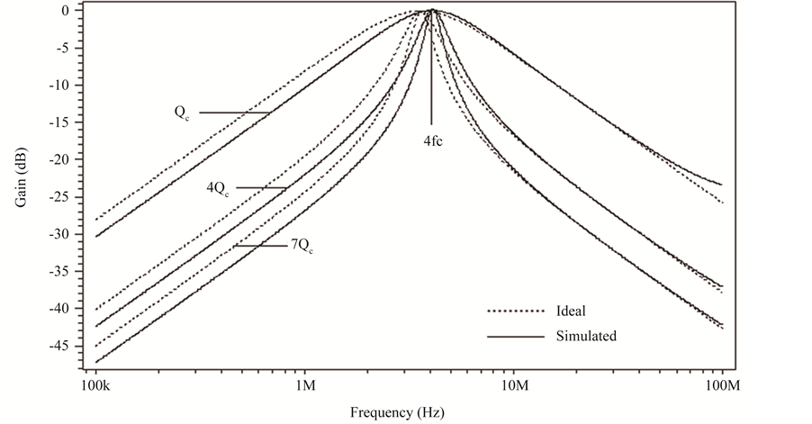
and . Pole frequency programming as described by Equation (6a) is performed by varying K2(=K3). Figure 3 shows the ω0 programming (in range 900 KHz to 6.3 MHz) of various responses for appropriate Q-values. Q-values are chosen depending on the type of response. Similarly Q-pro- gramming using codeword K1 (Equation 6(b)) is depicted in Figure 4. Codeword programming used in simulation is depicted in Table 4 and the corresponding filter parameters values are indicated in figures (Figure 3, Figure 4) itself. Figure 5 shows the time domain input and output waveforms to demonstrate the dynamic range of proposed DPUF for BP response. It is obtained by applying 300 mV peak sine wave of frequency 4fc. Figure 6 shows the variation of the total harmonic distortion (THD) with respect to the applied sinusoidal input voltage. The THD values of the circuit remains below 1% for input signal up to 300 mV peak.
 (a) (b)
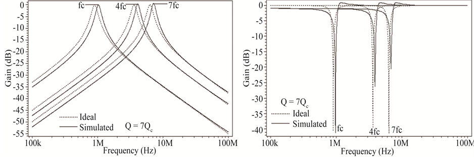 (c) (d)
Figure 3. (a) Pole frequency programming of LP response; (b) Pole frequency programming of HP response; (c) Pole frequency programming of BP response; (d) Pole frequency programming of BR response.
 (a)
(a) (b)
(b)
Figure 4. (a) Quality factor programming of BP response; (b) Quality factor programming of BR response.
Table 4. Codeword programming used in simulation.

Figure 5. Time response of BP response.

Figure 6. THD variation with respect to input sine wave signal.
7. Conclusion
This paper presents three VM DPUF configurations using least possible number of active and passive components. All DPUFs provide common attractive features such as the realization of four filter functions from same configurations, independently programmable filter parameters (ω0, Q) and no component matching constraint. Programmable characteristic of DPUF may be useful for various applications in mixed mode (analog/digital) VLSI system. All the circuits are realized and simulated by using 0.25 μm TSMC technology parameters.
Cite this paper
DeveshSingh,NeeloferAfzal,DineshPrasad,RichaSrivastava,KuldeepPanwar, (2015) Digitally Programmable Voltage Mode Universal Filters—A Minimal Realization. Circuits and Systems,06,213-223. doi: 10.4236/cs.2015.610022
References
- 1. Singh, D. and Afzal, N. (2013) Digitally Programmable High-Q Voltage Mode Universal Filter. Radioengineering, 22, 995-1006.
- 2. Hassan, T.M. and Mahmoud, S.A. (2009) Fully Programmable Universal Filter with Independent Gain-ω0-Q Control Based on New Digitally Programmable CMOS CCII. Journal of Circuits, Systems, and Computers, 18, 875-897.
http://dx.doi.org/10.1142/S0218126609005411 - 3. Alzaher, H., Tasadduq, N., Al-Ees, O. and Al-Ammari, F. (2013) A Complementary Metal-Oxide Semiconductor Digitally Programmable Current Conveyor. International Journal of Circuit Theory and Application, 41, 69-81.
- 4. El-Adawy, A.A., Soliman, A.M. and Elwan, H.O. (2002) Low Voltage Digitally Controlled CMOS Current Conveyor. International Journal of Electronics and Communication, 56, 137-144.
http://dx.doi.org/10.1078/1434-8411-54100086 - 5. Biolek, D., Senani, R., Biloekova, V. and Kolka, Z. (2008) Active Elements for Analog Signal Processing: Classification, Review, and New Proposals. Radioengineering, 17, 15-32.
- 6. Pun, K.P., Choy, C.S., Chan, C.F. and da Franca, J.E. (2003) Digital Frequency Tuning Technique Based on Current Division for Integrated Active RC Filters. Electronics Letters, 39, 1366-1367.
http://dx.doi.org/10.1049/el:20030911 - 7. Sedra, A. and Smith, K.C. (1970) A Second Generation Current Conveyor and Its Applications. IEEE Transaction on Circuit Theory, 17, 132-134.
http://dx.doi.org/10.1109/TCT.1970.1083067 - 8. Ferri, G. and Guerrini, N.C. (2003) Low-Voltage Low-Power CMOS Current Conveyors. Kluwer Academic Publishers, Boston.
- 9. Bhushan, M. and Newcomb, R. (1967) Grounding of Capacitors in Integrated Circuits. Electronics Letters, 3, 148-149.
http://dx.doi.org/10.1049/el:19670114 - 10. Baker, R.J., Li, H.W. and Boyce, D.E. (1998) CMOS Circuit Design, Layout, and Simulation. IEEE Press, New York.
- 11. Soliman, A.M. and Eman, A.S. (2013) Digitally Programmable Second Generation Current Conveyor-Based FPAA. International Journal of Circuit Theory and Application, 41, 1074-1084.
http://dx.doi.org/10.1002/cta.1826 - 12. Tangsrirat, W., Prasertsom, D. and Surakampontorn, W. (2009) Low-Voltage Digitally Controlled Current Differencing Buffered Amplifier and Its Application. International Journal of Electronics and Communication, 63, 249-258.
http://dx.doi.org/10.1016/j.aeue.2008.01.006 - 13. Singh, D. and Afzal, N. (2015) Digitally Programmable Current Conveyor Based Mixed Mode Universal Filter. International Journal of Electronics Letters, 3, 170-185.
http://dx.doi.org/10.1080/21681724.2014.917714 - 14. Alzaher, H.A. (2008) A CMOS Digitally Programmable Universal Current-Mode Filter. IEEE Transaction on Circuit and System-II, 55, 758-762.
http://dx.doi.org/10.1109/TCSII.2008.921599 - 15. Alzaher, H.A. (2008) A CMOS Digitally Programmable Filter Technique for VLSI Applications. Analog Integrated Circuit Signal Processing, 55, 177-187.
http://dx.doi.org/10.1007/s10470-008-9154-0 - 16. Alzaher, H., Tasadduq, N. and Al-Ees, O. (2012) A Class of Digitally Programmable nth-Order Filters. International Journal of Circuit Theory and Application, 40, 943-956.
http://dx.doi.org/10.1002/cta.764 - 17. Khan, I.A. and Nahhas, A.M. (2012) Current Mode Programmable Analog Modules Using Low Voltage Digitally Controlled CMOS CCII. International Journal of Computer Applications, 48, 38-44.
- 18. Alzaher, H., Tasadduq, N. and Al-Ees, O. (2013) Implementation of Reconfigurable nth-Order Filter Based on CCII. Analog Integrated Circuit Signal Processing, 75, 539-545.
http://dx.doi.org/10.1007/s10470-013-0064-4 - 19. Khan, I.A., Khan, M.R. and Afzal, N. (2006) Digitally Programmable Multifunctional Current Mode Filter Using CCIIs. Journal of Active and Passive Electronic Devices, 1, 213-220.
NOTES

*Corresponding author.