Circuits and Systems Vol.06 No.02(2015), Article ID:54118,18 pages
10.4236/cs.2015.62004
Design and Implementation of Low-Pass, High-Pass and Band-Pass Finite Impulse Response (FIR) Filters Using FPGA
Emmanuel S. Kolawole, Warsame H. Ali, Penrose Cofie, John Fuller, C. Tolliver, Pamela Obiomon
Department of Electrical and Computer Engineering, Prairie View A&M University, Prairie View, USA
Email: ekolawole@student.pvamu.edu, whali@pvamu.edu, pscofie@pvamu.edu, jhfuller@pvamu.edu, pobiomon@pvamu.edu
Copyright © 2015 by authors and Scientific Research Publishing Inc.
This work is licensed under the Creative Commons Attribution International License (CC BY).
http://creativecommons.org/licenses/by/4.0/


Received 1 February 2015; accepted 15 February 2015; published 15 February 2015
ABSTRACT
This paper presents the design and implementation of a low-pass, high-pass and a hand-pass Finite Impulse Response (FIR) Filter using SPARTAN-6 Field Programmable Gate Array (FPGA) device. The filter performance is tested using Filter Design and Analysis (FDA) and FIR tools from Mathworks. The FDA Tool is used to define the filter order and coefficients, and the FIR tool is used for Simulink simulation. The FPGA implementation is carried out using Spartan-6 LX75T-3FGG676C for different filter specifications and simulated with the help of Xilinx ISE (Integrated Software Environment). System Generator ISE design suit 14.6i is used in synthesizing and co-simulation for FPGA filter output verification. Finally, comparison is done between the results obtained from the software simulations and those from FPGA using hardware co-simulation. The simulation waveforms and synthesis reports verify the parallel implementation of FPGA which proves its effectiveness in terms of speed, resource usage and power consumption.
Keywords:
Digital Filters, FIR Filter, Matlab Simulink, FDA Tool, FIR Tool, Distributed Arithmetic, FPGA, Xilinx System Generator

1. Introduction
In signal processing, the function of a filter is to remove unwanted parts of the signal, such as random noise, or to extract useful parts of the signal, such as the components lying within a certain frequency range [1] . The FIR filter block diagram is as shown in Figure 1 [10] .
An ideal filter is a network that allows signals of only certain frequencies to pass while blocking all others. Depending on the region of frequencies that are allowed through or not, filters are characterized as low-pass, high-pass, band-pass, band-reject and all-pass. There are many needs for electric filters, some of the more common being those used in radio and television sets, which allow tuning into a certain channel by passing its band of frequencies while filtering out those of other channels [2] .
The FIR filters are widely used in signal processing and can be implemented using programmable digital processors. Due to the high performance requirements and increasing complexity of DSP and multimedia communication applications, filters with a large number of taps are required to increase the performance in terms of high sampling rate. As a result, the filtering operations are computationally intensive and more complex in terms of hardware requirements [3] . The FIR filters perform the weighted summations of input sequences with constant coefficients in most of the signal processing and multimedia applications. The FIR filter is a digital filter widely used in Digital Signal processing applications in various fields like imaging, instrumentation and communications. Programmable digital processor signal (PDPS) can be used in implementing the FIR filter. Nowadays, to make a difference on the market, new industrial control systems have to be highly performing, very flexible and reliable. At the same time, the cost is a key issue.
In order to reduce the cost, time-to-market has to be shortened, the price of a controller device has to be cheap and its energy consumption needs to be reduced [4] . This cost reduction is all the more challenging that new industrial control systems are based on ever increasing sophisticated control algorithms which need a lot of computing resources and need reduced execution time. However, in realizing a large order filter many complex computations are needed which invariably affect the general performance of the common digital signal processors in terms of speed, cost flexibility, stability and so on.
To cope with all these challenges, designers rely more on mature digital electronics technologies that come with friendly software development tools. Following this development, a Field-Programmable Gate Array (FPGA) has become an extremely cost-effective means of realizing computationally intensive digital signal processing algorithms to improve overall system performance.
The FIR filter implementation in FPGA utilizing the dedicated hardware resources can effectively achieve application-specific integrated circuit (ASIC)-like performance while reducing development time cost and risks [4] [5] . Hence, FPGA has become the best choice for the design of signal processing system due to its greater flexibility and higher bandwidth.
In this paper FDA tool from Matlab mathematical computational package with digital signal processing toolboxes is used to design filter response and generate coefficients tables. In the proposed approach, FIR tool utilizes distributed arithmetic (DA) as shown in Figure 2 which actually uses lookup table for storing constant coefficients. So, the use of lookup tables reduces the hardware complexity and hence the new design is more efficient in terms of less area, more speed and low power consumption due to its parallel implementation on FPGA, unlike the traditional DSP that utilizes MAC (unit multiplier and add accumulator) which increases memory resources as filter order increases [6] . System Generator package provided by Xilinx is used for FPGA implementation of each filter specification. The overall filter output waveforms and synthesis reports performances under parallel implementation of FPGA are greatly enhanced with the proposed method.
2. FIR Filters Design
・ It meets specifications with the least number of coefficients;
・ Uses less amount of resources on FPGA for implementation;
・ The weighted approximation error between the desired and actual frequency response is spread evenly across the pass-band and stop-band of the filter thereby minimizing error;
・ Pass-band and stop-band deviations can be specified separately.
Below is the Equiripple equation:

Figure 1. A block diagram of a FIR filter [10] .
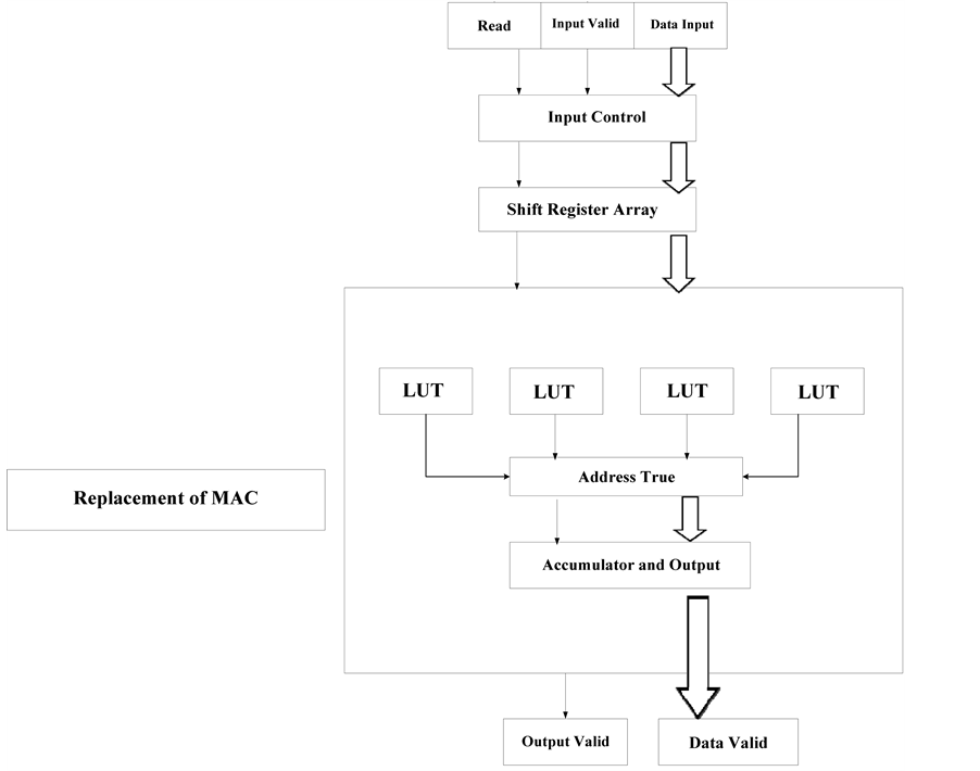
Figure 2. Implementation of FIR filter using DA [6] .
 (1)
(1)
where:
 is the best
approximation frequency response;
is the best
approximation frequency response;
 is the ideal
frequency response;
is the ideal
frequency response;
 is the weighting
function;
is the weighting
function;
 is the Equiripple
factor.
is the Equiripple
factor.
Table 1 as shown below elaborates the specifications of low-pass, high-pass and band-pass filters used in this paper:
Fs is the sampling frequency;
F-stop is the stop-band frequency;
F-pass is the pass-band frequency;
A-pass is the pass-band attenuation;
A-stop is the stop-band attenuation.

Table 1. FIR filters specifications.
FIRs have the advantage of being much more realizable in hardware [7] because they
avoid division and feedback paths. FIR filter response
 is computed by operation between filter coefficients
 and the data input
 as shown by the equation:
 (2)
(2)
where
 the filter
input;
the filter
input;
 the filter
coefficients;
the filter
coefficients;
 the filter
output;
the filter
output;
 the number
of filter coefficients (order of filter).
the number
of filter coefficients (order of filter).
The value of the constant k is a minimum value for which the expression
 is valid.
 .
.
where the operator
 represents rounding down to a less value.
In FIR filter design, filter frequency response coefficients and the corresponding window type function must be known before filter hardware realization. Table 2 shows the transfer function equations used in different types of filters [8] .
The value of variable n ranges between 0 and N, where N is the filter order. A constant
M can be expressed as .
Also
.
Also .
Since the variable n ranges from 0 and N, the ideal filter frequency response has
N + 1 sample.
.
Since the variable n ranges from 0 and N, the ideal filter frequency response has
N + 1 sample.
 is
the frequency response of each individual filter classification to be designed:
low-pass, high- pass or band-pass filter.
is
the frequency response of each individual filter classification to be designed:
low-pass, high- pass or band-pass filter.
The FIR filter coefficients are found using the following expression:
 (3)
(3)
For direct realization of FIR filter, it is based on the direct implementation of this expression:
 (4)
(4)
 is
the window function coefficients. In this design, Hamming window function is used
based on the filter specification. For Hamming window, the expression for
is
the window function coefficients. In this design, Hamming window function is used
based on the filter specification. For Hamming window, the expression for
 is given as;
 (5)
(5)
The FIR filter is graphically represented by a direct form approach [7] as shown in Figure 3. This graphical filter design approach using Equiripple method enhances easy selections for specifying passband, filter order, and design methods, as well as provides filter response of individual specification. The FDA Tool from Mathworks as shown for low-pass filter in Figure 4 is used to generate MATLAB model design and coefficient tables
Table 2. The frequency responses of standard ideal filters [8] .

Figure 3. The direct architecture of a typical FIR filter [7] .
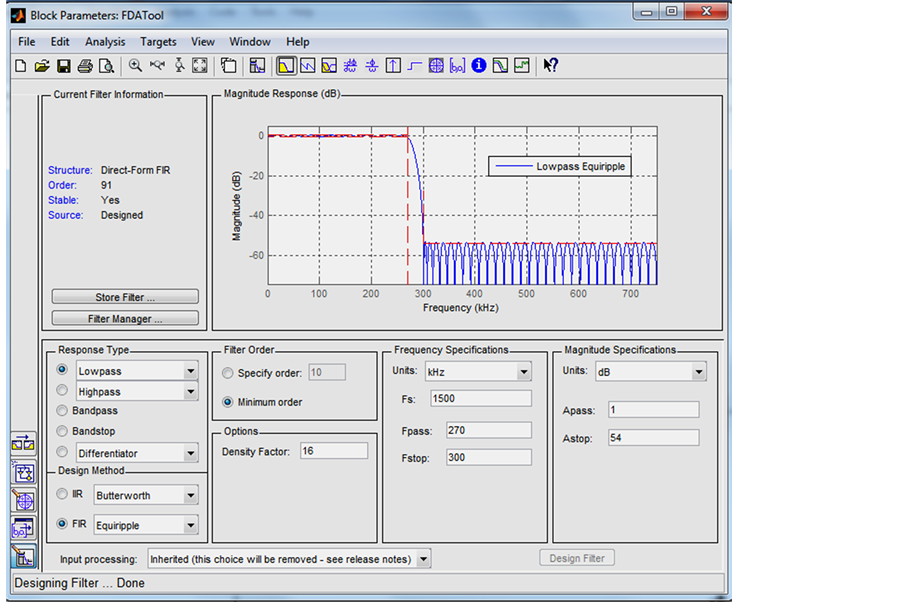
Figure 4. Low-pass filter using FDA Tool.
based on specification. Following the same procedure, high-pass and band-pass filters are equally generated based on their specifications.
3. FPGA Implementation of FIR Filter
After designing the filters based on their specifications from Matlab, the Xilinx software package provided by Spartan-6 FPGA board, System Generator is then used for the appropriate FIR FPGA filter implementation for low-pass, high-pass, band-pass filter as shown in Figures 5-9.
3.1. Simulation Results for Low-Pass FIR Filter
Figure 6(b) and Figure
6(c) verified the comparison between the low-pass filter simulation from
Matlab and FPGA implementation. Figure 6(a) is
the Input signal below
 using chirp source. Where
 is the cut-off frequency.
Figures 6(d)-(f) analyzed when the input signal is above the cut-off frequency and no output waveforms for low-pass frequency.
Figure 7 displays the FPGA implementation on high-pass filter while the corresponding Figure 8(b) and Figure 8(c) verify the comparison between the high-pass filter simulation from Matlab and FPGA implementation. Figure 8(a) is the input signal using chirp source when the signal is above the cut-off frequency.
3.2. Simulation Results for High-Pass FIR Filter
Figures 8(d)-(f) represent the output waveforms from Matlab and FPGA for High-pass
when the input signal is below .
High-pass did not pass at low frequency.
.
High-pass did not pass at low frequency.
Figure 9 displays the FPGA implementation on band-pass
filter while the corresponding Figure 10(b) and
Figure 10(c) verify the comparison between the
band-pass filter simulation from Matlab and FPGA implementation.
Figure 10(a) is the input signal using chirp source when the signals are
between
 and
and .
Band- pass passes frequency when the frequency is within the specified bandwidth.
.
Band- pass passes frequency when the frequency is within the specified bandwidth.

Figure 5. Low-pass FIR filter.
 (a)
(a) (b)
(b) (c)
(c) (d)
(d) (e)
(e) (f)
(f)
Figure 6. (a) Input signal below (FC) using chirp source; (b) Output waveform from low- pass FIR filter using Matlab; (c) Output waveform from low-pass FIR filter using FPGA; (d) Input signal above (FC) using chirp source; (e) Output waveform from low-pass FIR filter using Matlab; (f) Output waveform from low-pass filter using FPGA.
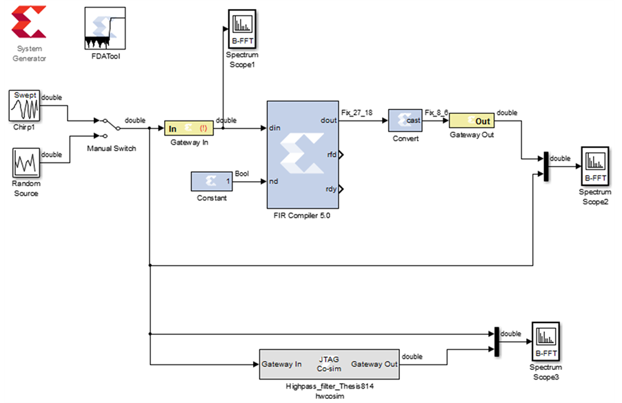
Figure 7. High-pass FIR filter.
3.3. Simulation Results for Band-Pass FIR Filter
Figures 10(d)-(f) represent the output waveforms from Matlab and FPGA for band-pass
when the input signal is below .
Band-pass did not pass at frequency lower that
.
Band-pass did not pass at frequency lower that .
.
Figures 10(g)-(i) represent the output waveforms from Matlab and FPGA for band-pass
when the input signal is below .
Band-pass did not pass at frequency above that
.
Band-pass did not pass at frequency above that .
.
4. Parallel Implementation on FPGA
Figure 11 identifies the true parallelism nature of FPGA, so different processing operations do not have to compete for the same resources. Each independent processing task is assigned to a dedicated section of the chip, and can function autonomously without any influence from other logic blocks [9] . As a result, the performance of one part of the application is not affected when more processing blocks are added [3] .
5. Simulation Results for Parallel Implementation
When the three filters were combined in parallel with individual specifications, the same output waveforms for all the filters were observed which actually proved the parallelism nature of FPGA. With input signal using random source as shown in Figures 12(a)-(g) verified the comparison between the low-pass, high-pass and band- pass filters simulations from Matlab and FPGA parallel implementation.
6. Discussions
In this paper, a ninety two-order low-pass and band-pass and ninety nine-order high-pass FIR filter have been implemented in Spartan-6 LX75T-3FGG676C FPGA board using Xilinx Integrated Software Environment (ISE). The propose idea gives an efficient approach towards the implementation of FIR filter using Simulink and subsequent synthesis on FPGA that suited different applications unlike most previous approaches on a penalty of reducing computation speed. Table 3 shows the comparison among the filters and their parallel implementation as drafted from the synthesis reports.
 (a)
(a) (b)
(b) (c)
(c) (d)
(d) (e)
(e) (f)
(f)
Figure 8. (a) Input signal above (FC) using chirp source; (b) Output waveform from high-pass FIR filter using Matlab; (c) Output waveform from high-pass FIR filter using FPGA; (d) Input signal below (FC) using chirp source; (e) Output waveform from high- pass FIR filter using Matlab; (f) Output waveform from high-pass filter using FPGA.
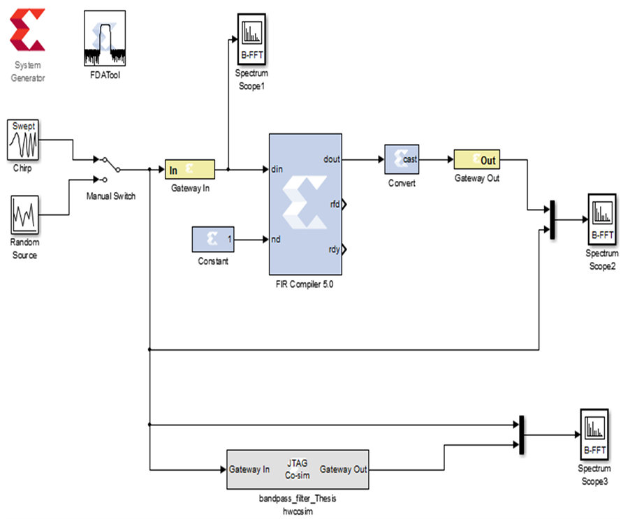
Figure 9. Band-pass FIR filter.
In addition, below are some of the factors used in evaluating the advantages of FPGA:
1) Time to market?FPGA technology offers flexibility and rapid prototyping capabilities in the face of increased time-to-market concerns. You can test an idea or concept and verify it in hardware without going through the long fabrication process of custom ASIC design. It is easy to implement incremental changes and iterate on an FPGA design within hours instead of weeks;
2) Cost?The nonrecurring engineering (NRE) expense of custom ASIC design far exceeds that of FPGA-based hardware solutions. With FPGA, it means that you have no fabrication costs or long lead times for assembly. This is because system requirements often change over time, the cost of making incremental changes to FPGA designs is negligible when compared to the large expense of re-designing an ASIC;
3) Long-term maintenance?As earlier discussed, FPGA chips are field-upgradable and do not require the time and expense involved with ASIC redesign. Digital communication protocols, for example, have specifications that can change over time, and ASIC-based interfaces may cause maintenance and forward-compatibility
 (a)
(a)
 (b)
(b) (c)
(c) (d)
(d) (e)
(e) (f)
(f) (g)
(g) (h)
(h) (i)
(i)
Figure 10. (a) Input
signal between
 and
and
 using chirp source; (b) Output waveform from band- pass FIR filter using Matlab;
(c) Output waveform from band-pass FIR filter using FPGA; (d) Input signal below
using chirp source; (b) Output waveform from band- pass FIR filter using Matlab;
(c) Output waveform from band-pass FIR filter using FPGA; (d) Input signal below
 using chirp source; (e) Output waveform from band-pass FIR filter using Matlab;
(f) Output waveform from band-pass filter using FPGA; (g) Input signal above
using chirp source; (e) Output waveform from band-pass FIR filter using Matlab;
(f) Output waveform from band-pass filter using FPGA; (g) Input signal above
 using chirp source; (h) Output waveform from band-pass FIR filter using Matlab;
(i) Output waveform from band-pass filter using FPGA.
using chirp source; (h) Output waveform from band-pass FIR filter using Matlab;
(i) Output waveform from band-pass filter using FPGA.
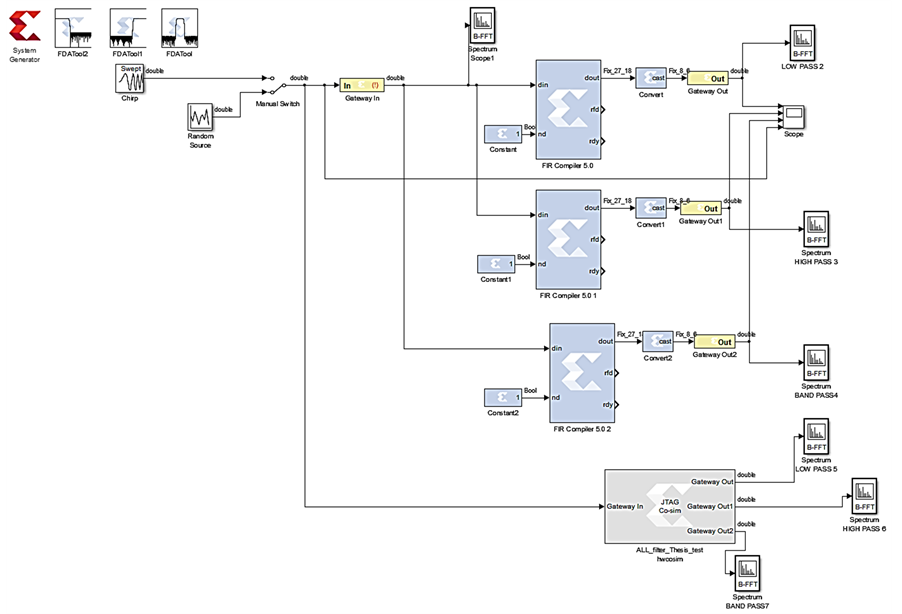
Figure 11. Parallel implementation of FIR filters.
Table 3. Comparison among filters.
challenges. Due to reconfigurable nature of FPGA chips, it can keep up with future modifications that might be necessary. As a product or system matures, you can make functional enhancements without spending time redesigning hardware or modifying the board layout;
4) Performance?The hardware parallelism nature of FPGAs exceed the computing power of digital signal processors (DSPs) by breaking the paradigm of sequential execution and accomplishing more per clock cycle. Controlling inputs and outputs (I/O) at the hardware level provides faster response times and specialized functionality to closely match application requirements. This again evaluates and validates the parallelism nature of FPGA;
5) Reliability?Due to the fact that software tools provide the programming environment, FPGA circuitry is truly a “hard” implementation of program execution. Processor-based systems often involve several layers of concept to help schedule tasks and share resources among multiple processes. For any given processor core, only one instruction can execute at a time, and processor-based systems are continually at risk of time-critical tasks preempting one another. Because FPGAs do not use OSs, it minimizes reliability concerns with true parallel execution and deterministic hardware dedicated to every task.
7. Conclusion
This paper discusses the implementation of low-pass, high-pass and band-pass FIR Digital Filters on a FPGA.
 (a)
(a) (b)
(b) (c)
(c) (d)
(d) (e)
(e) (f)
(f) (g)
(g)
Figure 12. (a) Input signal using Random source for parallel implementation; (b) Output waveform from low-pass FIR filter using Matlab; (c) Output waveform from low-pass filter using FPGA parallel implementation; (d) Output waveform from high-pass FIR filter using Matlab; (e) Output waveform from high-pass filter using FPGA parallel implementation; (f) Output waveform from band-pass FIR filter using Matlab; (g) Output waveform from band-pass filter using FPGA parallel implementation.
The simulation results show that the output waveforms obtained from the software simulations correspond with those from FPGA implementation respectively using hardware co-simulations. Also, the parallel implementation proves that performance of a low-pass filter is not affected by both high-pass and band-pass filter and vice-versa, and the synthesis report equally shows less resource usage, speed increase, cost effectiveness, more flexibility and low power consumption which validate the parallelism nature of FPGA.
References
- Ruan, A.W., Liao, Y.B. and Li, J.X. (2009) An ALU-Based Universal Architecture for FIR Filters. IEEE Proceedings of International Conference on communications, Circuits and Systems, Milpitas, July 2009, 1070-1073.
- Panayotatos, P. (2005) Frequency Response of Filters. Rutgers University, New Brunswick.
- Quayyum, A. and Mazher, M. (2012) Design of Programmable, Efficient Finite Impulse Response Filter Based on Distributive Arithmetic Algorithm. International Journal of Information Technology and Electrical Engineering, 1, 19-24.
- Monmasson, E., et al. (2011) FPGAs in Industrial Control Applications. IEEE Transactions on Industrial informatics, 7, 224-243. http://dx.doi.org/10.1109/TII.2011.2123908
- Wenjing, H., Guoyun, Z. and Waiyun, L. (2011) Self-Programmable Multipurpose Digital Filter Design Based on FPGA. IEEE Proceedings of International Conference on Internet Technology and Applications (iTAP), Wuhan, August 2011, 1-5.
- Mohanakrishnan, S. and joseph, B.E. (1995) Automatic Implementation of FIR Filters on Field Programmable Gate Arrays. IEEE Signal Processing Letters, 2, 51-53.
- Manal, H.J. and Asaad, H.S. (2013) High-Pass Digital Filter Implementation Using FPGA. IEEE International Journal of Advanced Computer Science and Applications (IJACSA), 13, 41-50.
- Abdullah, H.N. (2008) Design and Implementation of Programmable FIR Filter Using FPGA. Engineering and Technology Journal, 26.
- Xilinx White Paper Number 6984. www.xilinx.com
- Litwin, L. (2002) FIR and IIR Digital Filters. IEEE Potentials, 19, 28-31.