Circuits and Systems
Vol.05 No.11(2014), Article ID:50731,8 pages
10.4236/cs.2014.511028
On Design of Memristive Amplifier Circuits
Timur Ibrayev1, Irina Fedorova1, Akshay Kumar Maan2,3, Alex Pappachen James1*
1School of Engineering, Nazarbayev University, Astana, Republic of Kazakhstan
2Griffith University, Brisbane, Australia
3Enview R & D Labs, Trivandrum, India
Email: *apj@ieee.org
Copyright © 2014 by authors and Scientific Research Publishing Inc.
This work is licensed under the Creative Commons Attribution International License (CC BY).
http://creativecommons.org/licenses/by/4.0/

![]()

Received 18 August 2014; revised 22 September 2014; accepted 8 October 2014
ABSTRACT
Amplifiers are essential building blocks of a majority of the mixed signal circuits that are used in the development of cognitive computing architectures. Their implementation and use is chal- lenged by the second order effects that dominate the MOSFET operations with reduction in the technology size and scale. The ability to program the amplifiers once fabricated becomes an even more challenging problem as it warrants the use of multiple circuit components that lowers cir- cuit performance and in turn outweighs the advantages of generalisation abilities. In this paper, a reconfigurable set of amplifier circuits are proposed based on quantised conductance devices in combination with MOSFET devices. The presented circuits form the basic configurations for the memristor based amplifiers, and show promising performance results in terms of power dissipa- tion, on-chip area and THD values.
Keywords:
Resistive Switching, Memristive Device, Quantized Conductance, Common Source Amplifier, Common Drain Amplifier, Differential Amplifier

1. Introduction
The programmability of analog amplifiers is a challenging, and emerging topic of interest to developing circuits and systems required for futuristic neuromorphic computing architectures [1] [2] . Traditionally, the primary objective of the amplifiers has been to amplify the voltage or current signals and also to match the impedance be- tween circuits [3] - [5] . The ability to amplify signals is critical in sensory signal processing and neuromorphic networks to improve the quality and functionality of the modules. Neuromorphic networks are arranged in layers of neurons that are interconnected in an hierarchical manner, with the ability to transmit and transform the signal from input to output for a meaningful objective [6] - [8] . The ability of the networks to process the signals through learning weights over the connectivity between the network layers requires signal deformations to be minimal [9] - [11] . Increase in the number of the neurons and layers necessitates amplifiers to be integrated into the signal conditioning and processing stages of the neuronal circuit designs [12] - [15] . Since often the signal amplifications required are different for different layers of the network the amplifier designs would need to be tuned to fit into the signaling requirements for each layer [16] [17] . The problem becomes even more challeng- ing when the analog neuron networks are required to grow in size and functionality as the need for number of neurons increases with number of layers and inputs [18] [19] , which in turn puts additional burden on the need to ensure further signal conditioning to ensure accuracy and speed of learning.
Reconfigurability of the analog circuits in terms to adjusting the open loop gain and impedances offer the de- signers additional flexibility to improve the reliable operation of multilayered networks [20] - [22] . Similar to neuro- morphic networks, another example of application where they are vital is the memory processing and sensing [23] [24] . The analog to digital converters [25] [26] and data read/write circuits [27] make use of amplifiers that require different gains and bandwidths. While the goal is to ensure good performance with minimal change in design, the performance benchmarks drive designers to come up with significantly different circuit topologies for achieving parametric targets of gains, bandwidth and higher noise tolerance under low power conditions [28] . The objective of this paper is to advance the idea of programmability of amplifier circuits with very little modi- fication to circuit topology to ensure the structural and functional reproducibility of the amplifiers across the different layers of networks. To achieve this goal, we use simplistic amplifier configurations that make use of memristor like devices to configure the amplifier parameters. The low area requirements and low leakage cur- rents of memristor like devices followed up with the quantization of conductance with a memristive state enable programmability of the circuit.
2. Quantised Conductance Amplifier Configuration
Owing to increased second order effects and power considerations, current chip fabrication techniques are ap- proaching their fundamental limits. Resistive switching devices such as memristors offer a promising alternative as large scale, highly dense, programmable electronic memory network components [29] . Resistive switching enables quantised conductance by reversible formation and dissolution of nanometre-scale conductive filaments, which constrain the motion of electrons. Quantum effects begin to dominate and electron transport is quantised in multiples of the fundamental quantum of conductance  where e is the charge of electron and is Planck’s constant) [29] , thus leading to the resistive switching phenomenon where an external electric field coupled with the previous resistance state of the device determine the new resistance state.
The physical model of the memristor from [30] [31] shown in Figure 1 consists of a two-layer thin film size ( ) of
) of , sandwiched between platinum contacts. One of the layers doped with oxygen vacancies behaves as a semiconductor. The second, undopedregion, has an insulating property. As a consequence of quan- tised conductance process described above, the width w of the doped region is modulated depending on the amount of electric charge passing through the memristor. With electric current passing in a given direction, the boundary between the two regions is moving in the same direction. The total resistance of the memristor, M, is a sum of the resistances of the doped and undoped regions,
 (1)
(1)
where
![]() (2)
(2)
is the width of the doped region, referenced to the total length D of the ![]() layer, and
layer, and ![]() and
and ![]() are the values of the memristor resistance for
are the values of the memristor resistance for ![]() and
and![]() . The ratio of the two resistances is usually given as
. The ratio of the two resistances is usually given as ![]() [30] .
[30] .
The quantised conductance type [29] memristive devices offer different levels of conductance values within its state, that enables the discretized control of resistor values. Since resistors play a major role in the biasing and control of MOSFET amplifier parameters, the replacement of resistors with memristors can offer several advan- tages as compared to a resistor based design. The resistors in integrated circuits are implemented as semiconductor
resistors or as MOSFET pseudo-resistors that have a disadvantage of large reverse currents undesired in a resis- tor. In addition, a large resistance value is often associated with large area of semiconductor resistor or limited by the threshold voltage control in case of MOSFET pseudo-resistors. In contrast, quantised conductance me- mristors do not have the issue of reverse leakage currents and do not require to be scaled to achieve higher re- sistor values. The presented reconfigurable topology of common source, common drain and differential amplifier is built by using a combination of quantised conductance memristor like devices and MOSFET devices.
2.1. Common Source Amplifier
Figure 2 shows the common source amplifier that uses memristors ![]() and
and ![]() to form the memristive po- tential divider circuit to bias the transistor T, and
to form the memristive po- tential divider circuit to bias the transistor T, and ![]() controls the gain of the amplifier, and also plays a role in the output impedance of the amplifier. The open loop voltage gain of the amplifier is given as:
controls the gain of the amplifier, and also plays a role in the output impedance of the amplifier. The open loop voltage gain of the amplifier is given as:
 (3)
(3)
where  is the internal output resistance and
  is the transconductance of the MOSFET. Clearly, the ability to program the values of the
  enables the control of the amplifier open loop gain. The input resistance of the common source amplifier
  is defined in terms of the memristors
  and
and  and is expressed in the Equation (4).
 (4)
(4)

Figure 1. Memristor model [31] .

Figure 2. Circuit diagram of common source amplifier.
The output resistance of the circuit is given as:
 (5)
(5)
2.2. Common Drain Amplifier
Circuit of the common drain amplifier could be seen on Figure 3, where two memristors  and
and  are used in the same way as it was for the common source amplifier and
  is the variable memristance that is used for the control of the gain of the amplifier. The gain of the amplifier for the infinite output resistance
  is defined as follows:
 (6)
(6)
where rs is the reciprocal of the transconductance of the MOSFET .
.
Equation (6) shows that the gain of the common drain amplifier could be controlled by changing the values of the . Similar to the common source configuration the output resistance of the common drain is given as:
 (7)
(7)
The output resistance of the circuit is defined as:
 (8)
(8)
2.3. Differential Amplifer
Figure 4 represents the differential amplifier configuration with the variable memristive element  Tran- sistors
  and
and  as well as the other two transistors
  and
and  are in parallel.


Figure 3. Circuit diagram of common drain amplifier.
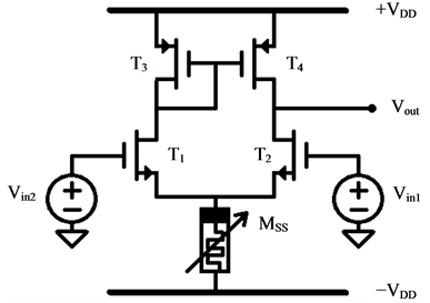
Figure 4. Circuit diagram of differential amplifier.
Common mode gain  for the differential pair is expressed as:
 (9)
(9)
where  is the single-ended output parameter and
  is the common mode input change. It could be further shown that:
 (10)
(10)
where  and
and  are the transconductance and output resistance of the transistors
  and
and  respec- tively and
  is the transconductance of the transistors
  and
and .
.
3. Experimental Results
The quantised conductance device offers different resistor values in its working states, and we make use of this to adjust the gain of the amplifiers. The ability of the memristor like devices to be programed to different logic state enable the practical realisation of these amplifiers as tunable open loop amplifiers within integrated circuits paradigm. Our quantised conductance memristive device offer resistances of 1.72 kΩ, 1.99 kΩ, 2.15 kΩ, 3.23 kΩ, 6.45 kΩ and 8.60 kΩ. The simulations were done using BSIM models and memristors SPICE model for si- mulating the quantized conductance devices. The parameters from the IBM process technology for different tech- nology size were used for the BSIM models to emulate realistic implementations.
Figure 5(a) shows the frequency response of the common source amplifier for discrete switching levels of memristive device for 0.18 μ technology of the transistor. The ability to change the resistance of the memristive device allows controlling the gain of the amplifier. Figure 5(b) shows the impact of technology scaling on the
 (a)
(a) (b)
(b)
Figure 5. (a) Graph for common source amplifier showing volatge gain for various values of MD; (b) Graph for common source amplifer showing voltage gain for various technologies at memristor value of MD = 1.72 kΩ.
frequency response for an example MD = 1.72 kΩ. Even with a large change in technology scales the bandwidth and gain is not compromised ensuring practical realisability in wide range of applications.
Figure 6(a) shows the change in gain magnitude of the common drain amplifier for the range of frequencies using different values of memristance for the 0.18 μ technology. Similar to the common source configuration, it is possible to control the voltage gain magnitude of common drain amplifier by implementation of memristor devices. Figure 6(b) shows the voltage gain magnitude at MS = 1.72 kΩ for the technologies having different scales. It can be seen that it is possible to have similar effect of memristor device despite the variations in tech- nology scales.
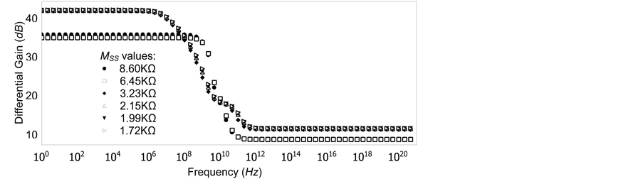
Figure 7(a) shows frequency response of the differential gain magnitude for various memristor device values MSS applied with the 0.18 μ technology of the transistors. The variations in the value of memristor device make it possible to alternate the value of the differential gain for the differential amplifier. Figure 7(b) shows the ef- fect of technology scaling on the differential gain magnitude at the MSS = 1.72 kΩ. Because of the similarity in gain magnitude and bandwidth, it is possible to have practical implementation of memristor devices in differen- tial amplifiers for different purposes.
Figure 8 shows the dependency of output resistance on memristance values for three different configurations. It could be observed that the results are in agreement with the corresponding equations describing behaviour of the amplifiers.
The circuit performance in terms of the area required for implementation of the circuit, power consumption and Total Harmonic Distortion (THD) for each of the three configurations are presented in Table 1. Area for common source, common drain and differential amplifiers were calculated taking into account each transistor and memristor of the circuit. These values are lower than that uses semiconductor resistors or pseudo-resistors of MOSFETs. In addition, the simplicity in the design without the need to increase the circuit complexity makes it a useful alternative in mainstream circuit design.
4. Conclusion
In this paper, we presented basic integrated amplifier circuits that is programmable for output signal gains using
 (a)
(a) (b)
(b)
Figure 6. (a) Graph for common drain amplifier showng volatge gain for various values of MS; (b) Graph for common drain amplifer showing voltage gain for various technologies at memristor value of MS = 1.72 kΩ.
 (a)
(a)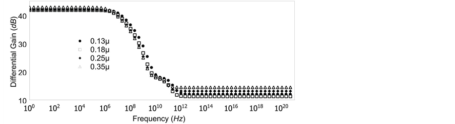 (b)
(b)
Figure 7. (a) Graph for differential amplifier showng volatge gain for various values of MSS; (b) Graph for differential amplifer showing voltage gain for various technologies at memristor value of MSS = 1.72 kΩ.

Figure 8. Graph showing output resistance versus memristance values for each of three amplifer.

Table 1. The table indicating the performance measures for different ampli- fier configurations able type.
aAssuming memristor dimensions to be 185 nm × 112 nm; bValues are taken at M = 1.72 kΩ; cInput is sine signal (amplitude = 1 V, frequency = 1 kHz); dInput is sine signal (amplitude = 10 mV, frequency = 1 kHz).
memristors like quantised conductance devices and MOSFET. The results of the simulations showed the im- proved performance of the common source, common drain and differential amplifiers in terms of the area, power and THD when implemented using the memristor elements instead of the conventional resistors or pseudo-resis- tors. The idea of controlling the resistance of the amplifier in an integrated circuit and the use of memristor ele- ment in the amplifier design is the new ideas suggested in this work. The proposed approach can have a wide- spread use in the implementation of analog amplifier circuits in sensory signal processing circuits, analog neu- romorphic networks, and memory driven circuits and systems.
References
- Rajendran, J., Manem, H., Karri, R. and Rose, G.S. (2010) Memristor Based Programmable Threshold Logic Array. Proceedings of the 2010 IEEE/ACM International Symposium on Nanoscale Architectures, Anaheim, 17-18 June 2010, 5-10. http://dx.doi.org/10.1109/NANOARCH.2010.5510933
- Ng, K.A. and Chan, P.K. (2005) A CMOS Analog Front-End IC for Portable EEG/ECG Monitoring Applications. IEEE Transactions on Circuits and Systems I: Regular Papers, 52, 2335-2347. http://dx.doi.org/10.1109/TCSI.2005.854141
- Mallinson, M. and Spitalny, P. (1993) Programmable Gain Amplifier. US Patent No. 5233309. US Patent and Trademark Office, Washington DC.
- Hall, T.S., et al. (2005) Large-Scale Field-Programmable Analog Arrays for Analog Signal Processing. IEEE Transactions on Circuits and Systems I: Regular Papers, 52, 2298-2307.
- Harrison, R.R., Bragg, J.A., Hasler, P., Minch, B.A. and Deweerth, S.P. (2001) A CMOS Programmable Analog Memory- Cell Array Using Floating-Gate Circuits. IEEE Transactions on Circuits and Systems II: Analog and Digital Signal Processing, 48, 4-11. http://dx.doi.org/10.1109/82.913181
- Türel, Ö. and Likharev, K. (2003) Cross Nets: Possible Neuromorphic Networks Based on Nanoscale Components. In- ternational Journal of Circuit Theory and Applications, 31, 37-53. http://dx.doi.org/10.1002/cta.223
- Afifi, A., Ayatollahi, A. and Raissi, F. (2009) STDP Implementation Using Memristive Nanodevice in CMOS-Nano Neuro- morphic Networks. IEICE Electronics Express, 6, 148-153. http://dx.doi.org/10.1587/elex.6.148
- Afifi, A., Ayatollahi, A. and Raissi, F. (2009) Implementation of Biologically Plausible Spiking Neural Network Models on the Memristor Crossbar-Based CMOS/Nano Circuits. European Conference on Circuit Theory and Design, ECCTD 2009, Antalya, 23-27 August 2009, 563-566.
- Turel, O., Lee, J.H., Ma, X. and Likharev, K.K. (2004) Nanoelectronic Neuromorphic Networks (Crossnets): New Re- sults. 2004 IEEE International Joint Conference on Neural Networks, Budapest, 25-29 July 2004.
- Likharev, K., Mayr, A., Muckra, I. and Türel, Ö. (2003) CrossNets: High-Performance Neuromorphic Architectures for CMOL Circuits. Annals of the New York Academy of Sciences, 1006, 146-163. http://dx.doi.org/10.1196/annals.1292.010
- Türel, Ö., Lee, J.H., Ma, X. and Likharev, K.K. (2004) Neuromorphic Architectures for Nanoelectronic Circuits. International Journal of Circuit Theory and Applications, 32, 277-302. http://dx.doi.org/10.1002/cta.282
- Alspector, J. (1989) Neuromorphic Learning Networks. US Patent No. 4874963.
- Indiveri, G., Chicca, E. and Douglas, R.J. (2009) Artificial Cognitive Systems: From VLSI Networks of Spiking Neurons to Neuromorphic Cognition. Cognitive Computation, 1, 119-127. http://dx.doi.org/10.1007/s12559-008-9003-6
- Schemmel, J., Fieres, J. and Meier, K. (2008) Wafer-Scale Integration of Analog Neural Networks. IEEE International Joint Conference on Neural Networks, IJCNN 2008, Hong Kong, 1-8 June 2008, 431-438.
- Zacek, K. and Nikolic, L. Analog Neural Networks. Technical University in Brno, 611.
- Widrow, B., Rumelhart, D.E. and Lehr, M.A. (1994) Neural Networks: Applications in Industry, Business and Science. Communications of the ACM, 37, 93-105. http://dx.doi.org/10.1145/175247.175257
- Boser, B.E., Sackinger, E., Bromley, J., Le Cun, Y. and Jackel, L.D. (1991) An Analog neural Network Processor with Programmable Topology. IEEE Journal of Solid-State Circuits, 26, 2017-2025. http://dx.doi.org/10.1109/4.104196
- Schemmel, J., Hohmann, S., Meier, K. and Schürmann, F. (2004) A Mixed-Mode Analog Neural Network Using Cur- rent-Steering Synapses. Analog Integrated Circuits and Signal Processing, 38, 233-244. http://dx.doi.org/10.1023/B:ALOG.0000011170.92377.6e
- Adhikari, S.P., Yang, C., Kim, H. and Chua, L.O. (2012) Memristor Bridge Synapse-Based Neural Network and Its Learn- ing. IEEE Transactions on Neural Networks and Learning Systems, 23, 1426-1435. http://dx.doi.org/10.1109/TNNLS.2012.2204770
- Xiang, L., Yang, Z., Shujuan, W. and Guofu, Z. (2011) A Method for Analog Circuits Fault Diagnosis by Neural Network and Virtual Instruments. 2011 3rd International Workshop on Intelligent Systems and Applications (ISA), Wuhan, 28-29 May 2011, 1-5.
- Stoica, A., Keymeulen, D., Zebulum, R., Thakoor, A., Daud, T., Klimeck, Y., et al. (2000) Evolution of Analog Circuits on Field Programmable Transistor Arrays. The 2nd NASA/DoD Workshop on Evolvable Hardware, Palo Alto, 13- 15 July 2000, 99-108.
- Giannini, V., Craninckx, J., D’Amico, S. and Baschirotto, A. (2007) Flexible Baseband Analog Circuits for Software- Defined Radio Front-Ends. IEEE Journal of Solid-State Circuits, 42, 1501-1512. http://dx.doi.org/10.1109/JSSC.2007.899103
- El Gamal, A. and Eltoukhy, H. (2005) CMOS Image Sensors. IEEE Circuits and Devices Magazine, 21, 6-20. http://dx.doi.org/10.1109/MCD.2005.1438751
- Cabric, D., Mishra, S.M. and Brodersen, R.W. (2004) Implementation Issues in Spectrum Sensing for Cognitive Radios. Conference Record of the 38th Asilomar Conference on Signals, Systems and Computers, 1, 772-776.
- Le, B., Rondeau, T.W., Reed, J.H. and Bostian, C.W. (2005) Analog-to-Digital Converters. IEEE Signal Processing Magazine, 22, 69-77. http://dx.doi.org/10.1109/MSP.2005.1550190
- Overney, F., Rufenacht, A., Braun, J., Jeanneret, B. and Wright, P.S. (2011) Characterization of Metrological Grade Analog-to-Digital Converters Using a Programmable Josephson Voltage Standard. IEEE Transactions on Instrumentation and Measurement, 60, 2172-2177. http://dx.doi.org/10.1109/TIM.2011.2113950
- Fukami, S., Ishiwata, N., Numata, H., Ohshima, N., Sugibayashi, T. and Suzuki, T. (2011) Magnetic Memory Cell, Magnetic Random Access Memory, and Data Read/Write Method for Magnetic Random Access Memory. US Patent No. 7929342.
- McConaghy, T., Palmers, P., Steyaert, M. and Gielen, G.G. (2011) Trustworthy Genetic Programming-Based Synthesis of Analog Circuit Topologies Using Hierarchical Domain-Specific Building Blocks. IEEE Transactions on Evolutionary Computation, 15, 557-570. http://dx.doi.org/10.1109/TEVC.2010.2093581
- Mehonic, A., Vrajitoarea, A., Cueff, S., Hudziak, S., Howe, H., Labbé, C., et al. (2013) Quantum Conductance in Silicon Oxide Resistive Memory Devices. Scientific Reports, 3, Article No. 2708. http://dx.doi.org/10.1038/srep02708
- Biolek, Z., Biolek, D. and Biolková, V. (2009) SPICE Model of Memristor with Nonlinear Dopant Drift. Radioengineering, 18, 210-214.
- Strukov, D.B., Snider, G.S., Stewart, D.R. and Williams, R.S. (2008) The Missing Memristor Found. Nature, 453, 80- 83.
NOTES

*Corresponding author.