Circuits and Systems
Vol.5 No.8(2014), Article
ID:48611,10
pages
DOI:10.4236/cs.2014.58021
Low-Noise Front-End Receiver Dedicated to Biomedical Devices: NIRS Acquisition System
Ahmad Chaddad
University of Texas MD Anderson Cancer Center, Houston, USA
Email: Achaddad@mdanderson.org
Copyright © 2014 by author and Scientific Research Publishing Inc.
This work is licensed under the Creative Commons Attribution International License (CC BY).
http://creativecommons.org/licenses/by/4.0/


Received 15 June 2014; revised 20 July 2014; accepted 2 August 2014
ABSTRACT
This paper concerns the design and the implementation of a fully integrated front-end intended to Near-Infrared Spectroscopy System (NIRS) acquisition system. A low-noise transimpedance amplification (TIA) circuit followed by adjustable cut-off frequency and a low-pass filter (LPF) was implemented in order to decrease noise circuit of NIRS detectors. For TIA, a single ended common source, common gate input stage based on a cascode structure is used to get a higher gain-bandwidth closed-loop transimpedance amplifier. To enhance the circuit noise performance, a single feedback transistor technique is used, compared to passive feedback, to achieved high quality data from NIRS acquisition channel. The proposed LPF combines two control methods to adjust the low cut-off frequency. Simulation results show a TIA gain of 104.2 dBΩ, −3dB bandwidth of 19 MHz and an equivalent input noise current spectral density of 446 fA/√Hz. LPF filter exhibits a relatively constant noise 201nV/√Hz from 0 Hz to 700 KHz and linearity performance over its entire tuning range. The proposed front-end of NIRS preamplifier is implemented using 0.18 µm CMOS technology.
Keywords:NIRS, TIA, LPF, CMOS

1. Introduction
NIRS is a new medical device that can be used for monitoring and in several neurological diseases in the human brain. It is considered in many hospitals for brain functional imaging. Among the most used methods in the clinical setting is functional magnetic resonance imaging (fMRI) and positron emission tomography (PET) [1] [2] . Meanwhile, NIRS is increasingly recognized by clinicians and its use has enabled functional studies of most areas of the brain [3] -[6] . These studies focused on research for the prevention, assessment and treatment of strokes, observation of newborn and adult brains state, rehabilitation of the brain after strokes and it has been applied to study certain psychiatric disorders. NIRS works primarily by sensing the oxygen variation in the blood through the absorption of red and near-infrared light [7] [8] . In NIRS, a light with a wavelength ranging from 630 to 1000 nm is applied to the head and passed through the brain. The detected light is directly proportional to the amount of oxygen available, especially in regard to the density of the oxy-deoxyhemoglobin. However, the oxygen in the brain corresponds to the amount of blood. As the oxy-deoxyhemoglobin plays a role in the absorption and diffusion of light in the near infrared spectrum, the corresponding wavelengths can be determined. To process the light signal, a highly sensitive receiver is required. Avalanche photodiodes (APD) can be an excellent light detector for low-level light detection in the visible and near-infrared regions. Thus, the APD fabricated are expensive and need high-voltage operation. These latter can be solved by using a standard CMOS process which is cheap and more efficient. By using CMOS technology, we can have the APD, TIA and LPF circuitries all on the same chip as an integrated system [9] . An APD is connected to the input of the optical receiver in reverse-biasing. It is used to sense the optical signal i.e. the light reflected from the cortex and to convert it to an electrical signal [10] -[12] . It absorbs incident radiation and generates an input current to the receiver. Usually, the NIRS acquisition channel contains an avalanche photodiode connected to the input of a preamplifier called a transimpedance. It plays a critical role in determining the numerous receiver aspects in term of performances and sensitivity. The NIRS system consists of near light sources, photo detectors, an amplifier followed by a filter in data acquisition system and a process unit (see Figure 1). In this paper, we present the transimpedance amplifier (TIA) followed by a low-pass filter, which are forming the front-end of the data acquisition system of a typical NIRS receiver. Moreover, the receiver sensitivity depends on input capacitor and built in preamplifier [13] . The four preamplifier topologies used in the optical receiver are the low-resistor terminal, the high impedance, the transimpedance, and the distributed amplifiers [14] . The trans-impedance amplifier is commonly used in optical receivers due to its ability to provide high transimpedance gain, wide bandwidth, low-input referred noise and low input impedance. The conventional designed circuits are common source, common drain or common gate followed by a source follower stage with large resistor feedback from the output to the input [15] . The parasitic capacitor of the photodiode directly affects the bandwidth and the input noise of the circuit. To minimize the effectiveness of the parasitic capacity at the receiver input several CMOS circuit techniques have been proposed, including the regulated cascode topology configuration [16] [17] . The drawbacks of these topologies are mainly in the input noise and the TIA gain performance. In order to enhance NIRS acquisition channel performance we proposed a TIA structure that uses a feedback transistor and a tunable low-pass filter. TIA is used to decrease the equivalent current input noise and increase dynamic range with circuit stability preservation. Additionally, the most used types of analog filters use two tunable active components, MOSFET-C and transconductance-C filters (Gm-C) [18] [19] . Recently, continuous time filter design, Gm-C, has been investigated in more details because of its continuous time signal processing and its lack of need for an anti-aliasing filter. Moreover, Gm-C filter design can integrate all of its building blocks into a single integrated circuit. The standard acquisition system like NIRS acquisition channel concerns the TIA, LPF and Analog to Digital Convertor (ADC) as shown in Figure 1. In our study, we focused on the TIA and LPF as two interesting electronic components for decrease the noise in preamplifier stage.
The remainder of this paper is organized as follows: section 2 presents the proposed TIA circuit including the transistor feedback as well as the calculation of the small signal of noise analysis for TIA, followed by the described of the proposed low-pass filter. Layout and simulation results are reported in section 3. Finally, the conclusion is given in section 4.
2. Materials and Methods
Integrated analog components within acquisition system play the initial role of the NIRS signal quality. TIA, LPF and analog to digital convertor (ADC) are the components of NIRS acquisition system. TIA is a one from the front-end part of the data acquisition system and its circuit in closed-loop as show in Figure 2(a) can be stated as follows:
 (1)
(1)
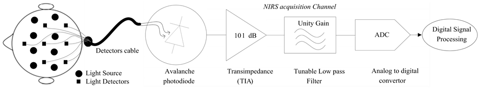
Figure 1. Block diagram of the proposed NIRS acquisition channels.
 (a)
(a)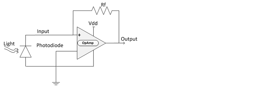 (b)
(b)
Figure 2. The proposed transimpedance amplification circuit. (a) Block diagram of the optical receiver front-end; (b) Proposed integrated transimpedance amplification circuit.
 is the output voltage,
  is the input current,
  is the transimpedance gain and
  is the feedback resistor.
When the photodiode is connected to the input of the TIA, the current of the photodiode is split between the amplifier and the photodiode capacitor. The trans-impedance is expressed according to
 (2)
(2)
where  is the photodiode capacitor.
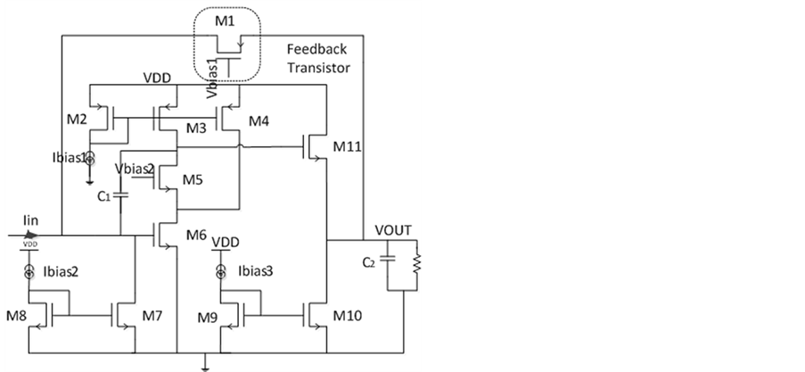
Integrated circuit of the transimpedance amplifier is presented in Figure 2(b). This latter concerns current mirror by two transistors (M7 and M8) to achieved low-input impedance at virtual ground (common mode voltage). It can effectively isolate the circuit from the parasitic capacitor of the photodiode to strongly reduce its effect on the bandwidth of the circuit. Miller capacitor compensation  is connected between the input and the output of the input stage for achieved the stability in a closed-loop. It has a very high gain stage, which is composed of a cascode common source and common gate amplifier. Input transistor size is chosen such that its gate and Miller capacitors make a good trade-off between wide bandwidth and best phase margin compensation. The dominant pole of the circuit depends on the gate and drain capacitors of the input transistor and the feedback PMOS transistor used to replace the standard feedback resistor
  of the TIA. This pole allows isolation of the photodiode parasitic capacitance depending on the cutoff −3dB frequency. The latter can be expressed according to
 (3)
(3)
where  and
and 
 is the gate capacitor of the input transistor,
  is the photodiode capacitor, A is the open-loop gain of the trans-impedance amplifier and,
  is the static resistor of the PMOS transistor, which can be expressed according to
 (4)
(4)
where  is the PMOS transistor size ratio,
  is the gate oxide capacitance,
 ![]() is the electron mobility,
is the electron mobility,  is the gate-source voltage and
  is the transistor threshold voltage.
In order to reduce the current input noise of the circuit, a small size of feedback transistor is chosen, it is inversely proportional to the static resistor and it can be expressed as following equation:
 (5)
(5)
Non-dominant pole of the circuit represented by the transistor drain and gate capacitors of the common gate amplifier. Consequently, this transistor size is selected to increase the total gain of the circuit and the frequency of the non-dominant pole in order to reduce signal dephasing and stability in closed-loops. The second branch of the input stage is designed to increase the inducing current for getting a high open-loop gain. Second stage is a source follower used as a level up shifter. It maintains a closed common mode DC voltage level at the output and input of the circuit in order to sustain DC stability in the closed-loop system. Finally, the capacitor and resistor load connected at the output of the circuit are used as a load and to compensate the phase margin of the circuit. Notice that the TIA can be computed according to
 (6)
(6)
where  is the total voltage gain of trans-impedance.
A transistor feedback system is proposed to highly reduce the input current referred noise of the circuit. It is based on a simple transistor used to replace the feedback resistor. Figure 2(a) shows the trans-impedance design with a feedback transistor where its feedback resistor value is based on the Rds feedback drain-source of transistor M1. Due to its large value [20] , equation (6) can confirm the reduction of the input current referred noise of the circuit. Based on a small signal model of a simple feedback transistor, the calculated feedback resistors  value can be expressed as following equation:
 (7)
(7)
where gds is the trans-conductance of transistor M1.
The linear relationship between the voltages of the transistor and the drain current are simplified as follows:
 (8)
(8)
The resistor  is inversely proportional of
 , and its resistor is controlled by the gate-source voltage, here it is controlled by
  as shown in Figure2(b).
Figure 3 shows the small signal model of the proposed TIA [20] . The current input noise can be computed by the following equations:
 (9)
(9)
 (10)
(10)
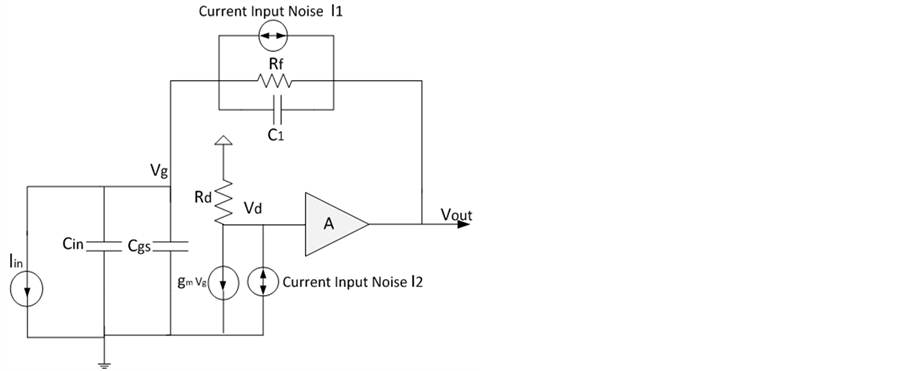
Figure 3. Small signal model of the proposed circuits for noise analysis.
 (11)
(11)
The current input noise of transistor M6 can be presented as follows:
 (12)
(12)
The total input referred noise is simplified as shown in equation (12).
 (13)
(13)
where  is the Boltzman constant,
 ![]() is closed-loop −3dB frequency,
is closed-loop −3dB frequency,  is the transconductance,
 ![]() is the mobility of the input transistor
is the mobility of the input transistor ,
,  in small signal noise analysis represents
  resistor for transistor
 .
.
A minimum transistor size is chosen in order to get high  value. However, the total input referred noise of the circuit with the simple transistor feedback is the sum of the source noise of the circuit including the feedback resistor
  (Current Input Noise
![]() ) and the input transistor
) and the input transistor , and it can be computed by the small signal model [20] as shown in Figure 3. Figure 4 (a) shows the conceptual schema of the operational amplifier (Opamp), the latter is a trans-conductance
 , and is followed by a tunable resistor
  and capacitor
 . The transfer function of this schema can be described according to
 (14)
(14)
where  is a variable resistor and
  is a variable capacitor.
From equation (14), we can express the cut-off frequency as presented in equation (15).
 (15)
(15)
We can determine the cut-off frequency by resistor and capacitor controlling as shown in equation (15). Figure 4(b) illustrates the schematic of a low-pass filter, where single stage architecture is shown. The latter re-
 (a)
(a)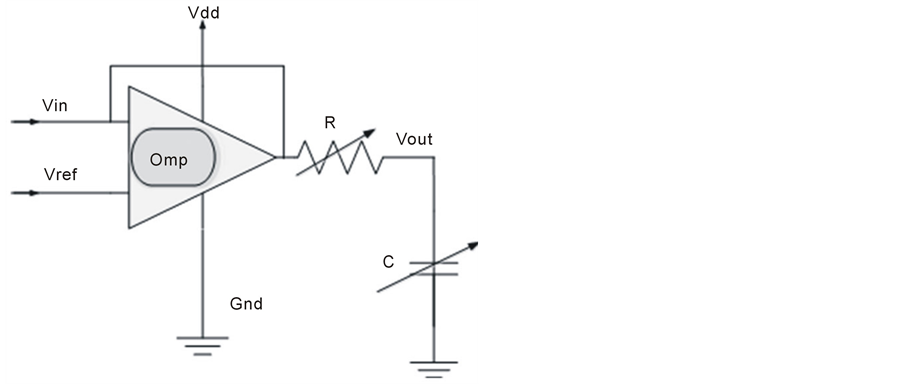 (b)
(b)
Figure 4. Schematic of a low-pass filter. (a) Simplified low-pass filter circuit; (b) Proposed integrated low-pass filter based on a tunable resistor and capacitor.
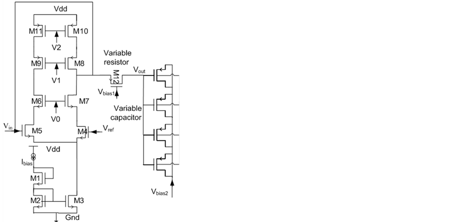
flects a low-power circuit topology for μw consumption, which is a main desired for embedded medical devices. It’s necessary in a portable medical system. Figure 4(a) showed the Opamp which is based on a telescopic topology like that shown in Figure 4(b).
All transistors are biased in the saturation region. Transistors M4-M5, M6-M7, M8-M9, M10-M11 and the tail current source represented in three transistors M1, M2 and M3, offer common-mode rejection, gain and frequency response. Transistor M12 represents the variable resistor controlled by bias voltage . Contrarily, the variable capacitor is represented in four identical transistors controlled by bias voltage
 .
.
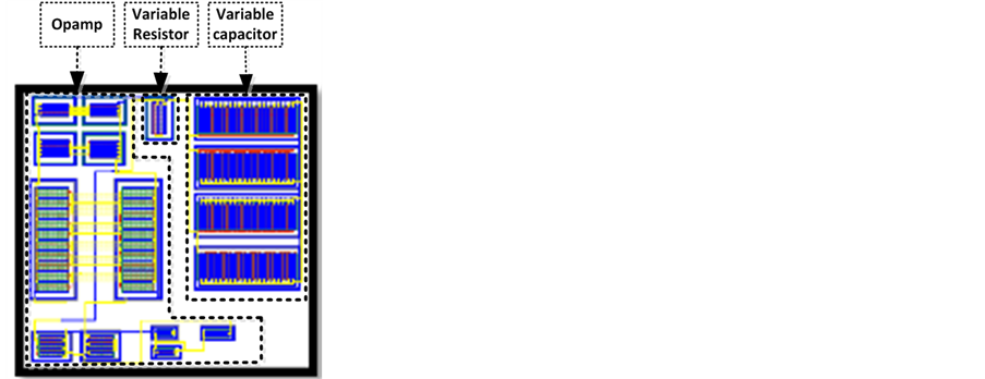
3. Experimental Results
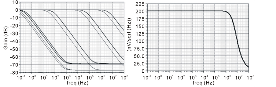
Circuits of the trans-impedance amplifier and low-pass filter are implemented in CMOS 0.18 µm. The simulation was done with Spectre using Cadence platform. Figure 5 illustrates the layout of both transimpedance and the low-pass filter. Simulation results of the layout are shown in Figure 6 which demonstrate a very good noise performance of the transimpedance amplifier when using the feedback of a PMOS transistor. The simulated value is 446 fA/√Hz @ 1 MHz. Consequently, this noise performance can improve signal-to-noise ratio of the NIRS acquisition channel. The simulated TIA gain and −3 dB bandwidth using feedback transistor was 101.2 dBΩ and 19 MHz respectively. This circuit has a power consumption of 940 mW. Figure 7 illustrates the simulated Bode transfer function of the TIA feedback transistor. Due to the large feedback drain-source resistors value, the circuit behaves like an open-loop and as shown in Figure 7 the simulated gain and phase margin values are 104.2 dBΩ and −71.58˚ respectively. Table 1 shows the performance and trade-offs of the proposed TIA topology with feedback transistor, and conventional topologies. The simulated input equivalent current spectral density and closed loop gain are 500fA/√Hz @ 10 kHz - 100 MHz and 101.2 dBΩ respectively. The latter exhibits high performance feature compared to the conventional topologies values as shown in Table1 In addition, the proposed topology has the ability to operate up to 10 GHz. The simulated results of LPF showed high performance in tunable cut-off frequency fc from 0 Hz to 100 MHz while exhibiting a constant power consumption of 212 µW. The proposed CMOS filter uses PMOS transistors in sub-threshold regime for implementing widely adjustable resistors and four identical transistors widely controlling capacitor values. The ultra-high resistivity of the resistor makes them suitable for implementing very-low frequency and compactfilters. Figure 8(a) illustrates the wide tunable cut-off frequency of the filter with variable curve degrees, with range of two control voltages  and
and  is from 0 to 1.2 V. Figure 8(b) shows the simulated input voltage noise from 0.1 Hz to 1MHz, the latter depending on the
  resistor in M12 Figure 4(b). We choose to compromise among the

Table 1 . Comparison of the proposed trans-impedance amplifier with conventional topologies.
**Measured; *Simulated.
 (a)
(a)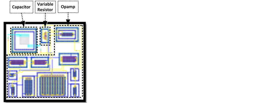 (b)
(b)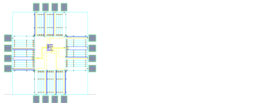 (c)
(c)
Figure 5. Layout of the proposed circuits with their area. (a) Full layout of integrated circuit; (b) Transimpedance circuit; (c) Low pass-filter. (a) Layout of the proposed TIA and LPF; (b) Transimpedance area is 0.0036 mm2; (c) Low pass-filter.
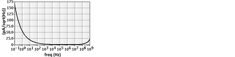
Figure 6. Simulation results of the transimpedance amplifier input referred noise.
constraints in order to get minimum noise and thus receive accurate medical diagnoses based on: miniaturized NIRS device, reduced power consumption, and minimized electronic component noise. Note that the miniaturization of NIRS device used a low power consumption which provides weak amplitude of NIRS signals however de noising signal can be help to obtain quality NIRS signals [25] -[27] .
4. Conclusion
In this paper, a low-noise front-end dedicated to near infrared spectroscopy applications has been implemented. A topology of transimpedance amplifier is presented, based on a bias input circuit with low-input impedance, which is connected to input stages to isolate the bandwidth dependency from the photodiode parasitic effect. Higher closedand open-loop gains were obtained by using a common source and common gate topology enhanced by a second active branch. To improve noise performance, we used a feedback transistor in order to en-
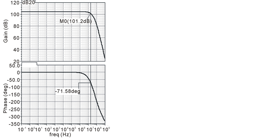
Figure 7. Simulation results of the transimpedance amplifier gain.
 (a) (b)
Figure 8. Simulation results of Low Pass Filter. (a) Cut-off frequency and curve degrees; (b) Input voltage noise of the opamp
hance the input noise performance. We presented a low-pass filter as a wide tunable cut-off frequency to match with input frequency signals from a photodiode. Layout simulation results showed that the TIA exhibit a lowinput referred noise, a high openand closed-loop transimpedance gain and low-power consumption compared to conventional topologies. As well as, the LPF showed a low-input voltage noise, wide tunable cut-off frequency and low-power consumption. Our TIA and LPF circuit can be implemented for most portable biomedical devices like EEG and ECG. The electronic analog circuits of TIA and LPF are relatively simple and can be easly connected with ADC to obtain NIRS signal.
Acknowledgements
Authors would like to acknowledge financial support from Canada Research Chair in Smart Medical Devices, and the design tools from CMC Microsystems.
References
- Mechelli, A., Friston, K.J. and Price, C.J. (2000) The Effects of Presentation Rate during Word and Pseudoword Reading: A Comparison of PET and fMRI. Journal of Cognitive Neuroscience, 12, 145-156. http://dx.doi.org/10.1162/089892900564000
- Pelletier, I., Paquette, N., Lepore, F., Rouleau, I., Sauerwein, C.H., Rosa, C., et al. (2011) Language Lateralization in Individuals with Callosal Agenesis: An fMRI Study. Neuropsychologia, 49, 1987-1995. http://dx.doi.org/10.1016/j.neuropsychologia.2011.03.028
- Lemm, S., Dickhaus, T., Blankertz, B. and Müller, K.R. (2011) Introduction to Machine Learning for Brain Imaging. NeuroImage, 56, 387-399. http://dx.doi.org/10.1016/j.neuroimage.2010.11.004
- Chaudhary, U., Hall, M., De Cerce, J., Rey, G. and Godavarty, A. (2011) Frontal Activation and Connectivity Using Near-Infrared Spectroscopy: Verbal Fluency Language Study. Brain Research Bulletin, 84, 197-205. http://dx.doi.org/10.1016/j.brainresbull.2011.01.002
- Dieler, A.C., Tupak, S.V. and Fallgatter, A.J. (2012) Functional Near-Infrared Spectroscopy for the Assessment of Speech Related Tasks. Brain Lang, 121, 90-109. http://dx.doi.org/10.1016/j.bandl.2011.03.005
- Quaresima, V., Bisconti, S. and Ferrari, M. (2012) A Brief Review on the Use of Functional Near-Infrared Spectroscopy (fNIRS) for Language Imaging Studies in Human Newborns and Adults. Brain Lang, 121, 79-89. http://dx.doi.org/10.1016/j.bandl.2011.03.009
- Lareau, E., Lesage, F., Pouliot, P., Nguyen, D., Le Lan, J. and Sawan, M. (2011) Multichannel Wearable System Dedicated for Simultaneous Electroencephalography/Near-Infrared Spectroscopy Real-Time Data Acquisitions. Journal of Biomedical Optics, 16.
- Cole Jr. AL., Herman, R.A., Heimlich, J.B., Ahsan, S., Freedman, B.A. and Shuler, MS. (2012) Ability of Near Infrared Spectroscopy to Measure Oxygenation in Isolated Upper Extremity Muscle Compartments. Journal of hand surgery, 37, 297-302. http://dx.doi.org/10.1016/j.jhsa.2011.10.037
- Bhattacharya, P. (1997) Semiconductor Optoelectronic Devices. 2nd Edition, Prentice-Hall, Inc., Upper Saddle River.
- Kamrani, E., Lesage, F. and Sawan, M. (2012) Premature Edge Breakdown Prevention Techniques in APD fabrication. The 10th IEEE International NEWCAS Conference (NEWCAS2012), Montreal, 17-20 June 2012, 345-348.
- Facpong Achigui, H. (2007) Conception d’amplificateurs opérationnels à basse tension pour des systèmes de dépistage de crises épileptiques. Library and Archives Canada, Ottawa.
- Achigui, H., Sawan, M. and Fayomi, C.J. (2008) A Monolithic Based NIRS Front-End Wireless Sensor. Microelectronics Journal, 39, 1209-1217. http://dx.doi.org/10.1016/j.mejo.2008.01.055
- Kasper, B.L. (1998) Chapter 18, Receiver Design. In: Miller, S.E. and Kaminow, I., Eds., Optical Fiber Telecommunications II, Academic Press, Inc., New Jersey.
- Tao, R., Berroth, M. and Wang, Z.G. (2004) Wide-Band Low-Power CMOS Transimpedance Preamplifier. IEEE MTT-S International Microwave Symposium Digest, 2, 983-985.
- Tao, R., Berroth, M. and Wang, Z.G. (2003) Monolithically Integrated CMOS Current-Mode Transimpedance. Electronics Letters, 39, 1772-1774. http://dx.doi.org/10.1049/el:20031174
- Park, S. and Toumazou, C. (2000) A Packaged Low-Noise High-Speed Regulated Cascode Transimpedance Amplifier Using a 0.61m n-Well Cmos Technology. Proceedings of European Solid-State Circuits Conference, Stockholm, 19-21 September 2000, 431-434.
- Hoyle, C. and Peyton, A. (1999) Shunt Bootstrapping Technique to Improve Bandwidth of Transimpedance Amplifiers. Electronics Letters, 35, 369-370. http://dx.doi.org/10.1049/el:19990290
- Ozalevli, E. and Hasler, P. (2005) Design of a CMOS Floating-Gate Resistor for Highly Linear Amplifier and MultiplierApplications. Proceedings of the Custom Integrated Circuits Conference, San Jose, California, 21 September 2005, 735-738.
- Vavelidis, K., Tsividis, Y.P., Eynde, F.O. and Papananos, Y. (1997) Six-Terminal MOSFET’s: Modeling and Applications in Highly Linear, Electronically Tunable Resistors. IEEE Journal of Solid-State Circuit, 32, 4-12. http://dx.doi.org/10.1109/4.553170
- Sedra, A. and Smith, K.C. (2010) Microlectronic Circuits. 6th Edition. Oxford University Press, New York.
- Wong, A.K.Y., Leung, K.N., Pun, K.P. and Zhang, Y.T. (2010) A 0.5-Hz High-Pass Cutoff Dual-Loop Transimpedance Amplifier for Wearable NIR Sensing Device. IEEE Transactions on Circuits and Systems, 57, 531-535.
- Sanz, M.T., del Pozo, J.M.G., Celma, S. and Sarmiento, A. (2007) 1.25 Gb/s Variable Transimpedance Amplifier in Digital CMOS Process. 50th Midwest Symposium on Circuits and Systems, MWSCAS, Montreal, 5-8 August 2007, 273-276.
- Park, S.M. and Yoo, H. (2004) 1.25-Gb/s Regulated Cascode CMOS Transimpedance Amplifier for Gigabit Ethernet Applications. IEEE Journal of Solid-State Circuits, 39, 112-121. http://dx.doi.org/10.1109/JSSC.2003.820884
- Zand, B., Phang, K. and John, D.A. (2001) A Transimpedance Amplifier With DC-Coupled Differential Photodiode Current Sensing for Wireless Optical Communications. IEEE Conference on Custom Integrated Circuits, San Diego, 6-9 May 2001, 455-458.
- Chaddad, A. (2014) Brain Function Diagnosis Enhanced Using Denoised fNIRS Raw Signals. Journal of Biomedical Science and Engineering, 7, 218-227. http://dx.doi.org/10.4236/jbise.2014.74025
- Chaddad, A. (2014) Brain Function Evaluation Using Enhanced fNIRS Signals Extraction. 48th Annual Conference on Information Sciences and Systems (CISS), Princeton, 19-21 March 2014, 1-4.
- Chaddad, A., Kamrani, E., Le Lan, J. and Sawan, M. (2013) Denoising fNIRS Signals to Enhance Brain Imaging Diagnosis. IEEE, 29th Southern Biomedical Engineering Conference, Miami, 3-5 May 2013, 33-34.