Circuits and Systems
Vol.5 No.4(2014), Article ID:44306,13 pages DOI:10.4236/cs.2014.54010
A 1-GHz, 7-mW, 8-Bit Subranging ADC without Resistor Ladder Using Built-In Threshold Calibration
Kenichi Ohhata*, Wataru Yoshimura, Daiki Tabira, Futoshi Shimozono, Masataro Iwamoto
Department of Electrical and Electronics Engineering, Graduate School of Science and Engineering, Kagoshima University, Kagoshima, Japan
Email: *k-ohhata@eee.kagoshima-u.ac.jp
Copyright © 2014 by authors and Scientific Research Publishing Inc.
This work is licensed under the Creative Commons Attribution International License (CC BY).
http://creativecommons.org/licenses/by/4.0/


Received 23 January 2014; revised 23 February 2014; accepted 5 March 2014
ABSTRACT
A subranging analog-to-digital converter (ADC) features high-speed and relatively low-power. The limiting factors of power reduction in subranging ADCs are the resistor ladder and the comparator. We propose an ADC architecture combining a capacitive digital-to-analog convertor and built-in threshold calibration to eliminate the resistor ladder, resulting in a low-power subranging ADC. We also propose a calibration technique comprising of metal-oxide-metal capacitor, MOS switch, and scaling capacitor to reduce the power consumption of the comparator and an offset drift compensation technique to enable precise foreground calibration. We designed an 8-bit, 1-GHz subranging ADC by applying these techniques, and post-layout simulation results demonstrated a power consumption of 7 mW and figure of merit of 51 fJ/conv.-step.
Keywords:Analog-to-Digital Convertor; Subranging Architecture; Resistor Ladder; Foreground Calibration; Offset Drift

1. Introduction
Power reduction in a medium resolution (6 - 8 bit) and high-speed (~1 GHz) analog-to-digital convertor (ADC) is strongly required for front end of wireless systems and read channels of disk systems. To meet this requirement, two approaches have been used so far. The first is based on parallel architecture suited for high-speed operation [1] -[7] . The main challenge in this approach is how power can be reduced while maintaining high-speed performance. The second approach is based on successive approximation register architecture suited for lowpower operation [8] -[11] . The main challenge in this approach is how operation speed can be improved while maintaining low-power operation. We previously studied the subranging architecture by using the latter approach and proposed a reference voltage precharging architecture [7] and a low-power high-resolution comparator using charge-steering amplifier [4] . There have been studies on high-performance subranging ADCs, e.g., a combination with the time-interleaving technique [5] , a reference voltage generator using a capacitive digitalto-analog converter (CDAC) [12] [13] and a low-power comparator using a digital foreground calibration technique [6] [14] . These studies resulted in high-speed and low-power 8-bit subranging ADCs with a sampling frequency of 1 GHz and figure of merit (FOM) of approximately 100 fJ/conv.-step [4] [6] . There are two powerdetermining factors in state-of-the-art subranging ADCs. The first is a resistor ladder as a reference voltage generator. A resistive ladder requires a large bias current to alleviate the effect of kickback noise from comparators; therefore, reducing the power dissipation is difficult [4] . The second is a comparator. Recently, low-power comparators could be realized using digital foreground calibration; however, there is room for further power reduction because power is wasted due to the large parasitic capacitance of the variable capacitor. Moreover, the digital foreground calibration has an issue of resolution degradation due to the offset drift. Recalibration is required when the temperature changes after calibration. Some applications cannot accept recalibration because AD conversion is suspended during recalibration.
We discuss two power-determining factors in a conventional technique in Section 2. We then propose a lowpower ADC architecture without a resistor ladder in Section 3 and propose circuit implementation techniques in Section 4. Finally, we explain the performances of a designed subranging ADC using the proposed techniques through post-layout simulations.
2. Conventional Technique
A block diagram of a conventional subranging ADC [15] is shown in Figure 1. This ADC comprises coarse and fine ADCs (CADC and FADC) and converts analog input (Vin) into digital outputs (Cout and Fout) in two stages. The analog input is sampled using a track and hold circuit (TH) and the sampled signal is first converted into an upper digital code by the CADC. The reference voltages for the CADC are generated using a coarse resistor ladder (RLC). Then, appropriate reference voltages (VrefT and VrefB) are selected using analog multiplexers (AMUX) on the basis of the CADC outputs. The reference voltages for the FADC are generated using a fine resistor ladder (RLF) from VrefT and VrefB and the FADC generates lower digital codes. The number of comparators is much smaller than that in a flash ADC because the conversion is executed in two steps; therefore, the power dissipation and the chip area can be reduced compared with a flash ADC. There are two bottlenecks to reducing power dissipation. The first is the resistor ladder. A large bias current is required for the resistor ladder to alleviate the effect of kickback noise from the comparators. Recently, a comparator has often comprised only an analog latch without preamplifiers to reduce the power dissipation. In this case, larger bias current is required because large kickback noise is generated by the analog latch. These situations prevent the resistor ladder from reducing power dissipation.
To overcome this problem, a built-in threshold technique using a capacitor [14] and reference voltage generation technique using a CDAC [12] [13] were proposed. With the latter technique, however, the input range was limited because adjustment range of the threshold voltage was small. The input range was only 200 mV [14] . The challenge in reference voltage generation using a CDAC is the gain variation of the CDAC. It has been reported that a gain variation of 15% degenerates the effect number of bit (ENOB) by 0.5 bit [16] . In this study, the ADC generated voltages corresponding to the top and bottom of the FADC input range by the CDAC, and the reference voltages for the FADC were generated by interpolating the top and bottom voltages. As shown in Figure 2, this 6-bit ADC comprises a 4-bit CADC and 3-bit FADC, and one-bit is for range overlapping. This ADC has two sets (ch.A and ch. B) of a CDAC and FADC for operation in two-way interleaving. The CDAC outputs the differences (VINPa and VINPb) between the input signal VINP and reference voltages (VREFPa and VREFPb) located up and down theVINP. The threshold voltage of the FADC is generated by interpolating VINPa and VINPb. Interpolation is done by changing the gate width of the input transistors (MPa and MPb) of the comparator. The interpolation relaxes the error due to the gain variation of the CDAC in this architecture. However, this ADC requires four CDACs in total; therefore, the overhead of the chip area and power dissipation is large.
The second bottleneck to power reduction is the comparator. The offset voltage of the comparator is determined by the threshold voltage mismatch of the input differential pair. The threshold voltage mismatch can be

Figure 1. A block diagram of a conventional subranging ADC.

Figure 2. A block diagram of a conventional subranging ADC using capacitive DAC.
reduced by enlarging the gate area; however, the gate area should be very large because the threshold voltage mismatch has only weak dependence on the gate area (proportional to gate area−1/2). Therefore, the digital calibration techniques were proposed to compensate for the offset of the comparator. Digital calibration cancels the mismatch due to process variation by intentionally introducing the opposite mismatch. Various mismatch introductions were proposed such as current, capacitance, and back bias [14] [17] [18] . The capacitance mismatch introduction is often used because of small noise and area. However, the comparator with this technique has large power dissipation and a narrow compensation range because the MOS variable capacitor has large parasitic capacitance.
3. Proposed ADC Architecture
The block diagram of the subranging ADC designed using the proposed architecture is shown in Figure 3. The ADC comprises a 4-bit CADC and 4.2-bit FADC and converts an analog input Vin into 8-bit digital codes DO<7:0>. The FADC has 19 comparators for a range overlapping of 2 LSB, each at the top and bottom of the input range of the FADC. The resistor ladder is eliminated; the threshold voltages of the comparators in the CADC and FADC are defined by the built-in threshold technique instead. The input signal of the FADC is generated by the CDAC. The CDAC samples the analog input signal then generates the residue signal subtracted the conversion result of CADC from the analog input signal. The residue signal is converted into lower 4-bit digital codes by the FADC. The timing chart of the designed ADC is also shown in Figure 3. The ADC has two sets of
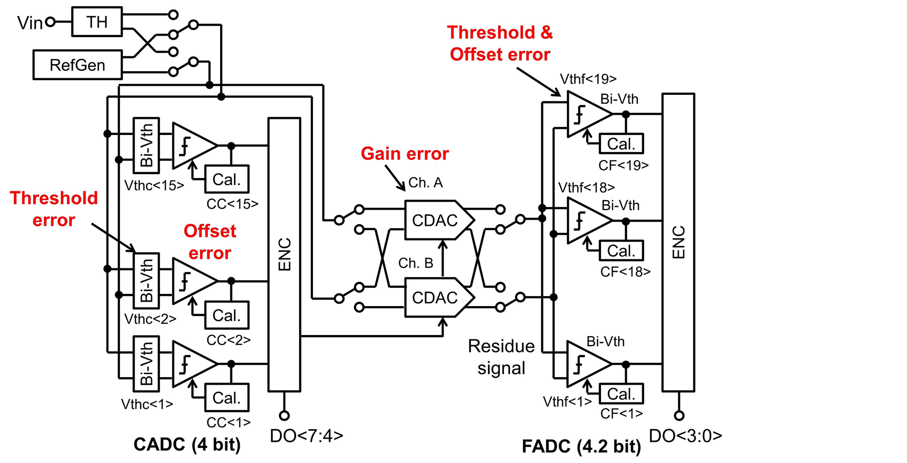

Figure 3. A block diagram and timing chart of proposed ADC.
CDACs (ch.A andch. B) and they operate in two-way interleaving. Therefore, the CADC, CDAC and FADC can use the half the cycle time, resulting in a sufficient timing margin. The error sources in this architecture are the gain error of the CDAC, the offset error of the comparator, and the built-in threshold error. Previous studies compensated for the gain error by using the interpolation technique; however, four CDACs were required to address the interpolation, resulting in large area overhead.
We solve this problem by adjusting the threshold voltages of the FADC in accordance with the gain error of the CDAC by using built-in threshold calibration technique. The calibration sequence in designed ADC is shown in Figure 4. Calibration is done individually for the comparators of the CADC and FADC. The TH is first disconnected from the CADC and FADC then a reference voltage generator (RefGen) is connected. The RefGen outputs Vthc<1> which is the threshold voltage of the 1st comparator of the CADC (CC<1>). The calibration circuit of CC<1> is then selectively activated. The calibration circuit adjusts the variable capacitor included in the comparator so that the threshold voltage of CC<1> is equal to Vthc<1>. Next, the RefGen outputs Vthc<2> which is the threshold voltage of the 2nd comparator CC<2>, and the same operation is repeated. Therefore, all comparators of the CADC are adjusted to the desired threshold voltage. With this technique, both the error due to the built-in threshold and the offset error are also adjusted, resulting in a precise threshold voltage. After CADC calibration, FADC calibration begins. The RefGen outputs Vthf<1> which is the threshold voltage of the 1st comparator of FADC (CF<1>) and the calibration circuit of CF<1> is selectively activated. At this time, all of the gain error of the CDAC, built-in threshold error and the offset error of CF<1>, are compensated because Vthf<1> passes through the CDAC. Therefore, the proposed ADC requires only two CDACs, resulting in a small chip area and low-power operation because interpolation is not required. Furthermore, the RefGen comprises a resistor ladder and selector circuit, and the bias current of the resistor ladder is provided only in the calibration mode. Therefore, the RefGendoes not consume power in normal operation.

Figure 4. Sequence of built-in threshold calibration.
4. Circuit Implementation
4.1. Built-In Threshold Circuits
Built-in threshold is not a novel technique because a flash ADC using this technique has been already reported [14] ; however, some considerations are required to apply it to subranging ADCs. A subranging ADC comprises a CADC with a wide input range and FADC with a narrow input range; therefore, appropriate built-in threshold implementation should be selected for each ADC. The method for changing the ratio of the sampling capacitance is used for the CADC and the method for changing the load capacitance is used for the FADC. Aschematic of the comparator with built-in threshold for the CADC is shown in Figure 5. The built-in threshold for the CADC is implemented by splitting the sampling capacitance into CT and CB and changing the ratio of (CT−CB)/(CT+CB) to handle a wide input range. The input signals INP and INN are connected to the sampling capacitors CT and CB in the sampling phase; therefore, the input signal is sampled by the sampling capacitors. The gate voltages of the input differential pair are set to a common voltage Vcom at this time. In the comparison phase, the switches are connected to VT and VB, which are the top and bottom voltages of the input range. Charge redistribution occurs at this time and the gate voltages of the input differential pair are changes around Vcom depending on the input signals. The threshold voltage is determined as follows.
 (1)
(1)
The threshold voltage can be changed in the range of VT−VB by changing CT and CB. The sampling switches do not consume power; however, the clock driver dissipates some power. The power dissipation of a comparator including the clock driver is only 30 μW at the operating frequency of 1 GHz.
The built-in threshold of the FADC can be obtained using a simpler method compared with the CADC, as shown in Figure 6, because the input range of the FADC is much smaller than that of the CADC. A capacitor Cbi is connected to one side drain node of the input differential pair. Positive threshold is generated when the Cbi is connected to the drain of the INP side. The threshold voltage is expressed as
 (2)
(2)
where Cp is the parasitic capacitance of the drain node and VOD is the overdrive voltage of the differential pair. The power dissipation increases in proportional to Cbi; however, the required Cbi is approximately 3 fF at most because the variable range of the threshold voltage of the FADC is ±25 mV. Therefore, power dissipation is sufficiently small (less than 20 μW).
4.2. Low-Power and High-Resolution Threshold Voltage Adjustment Technique
Various threshold voltage adjustment techniques for digital calibration have been proposed [19] . The common principle of these techniques is that the threshold voltage can be adjusted by introducing a kind of asymmetry

Figure 5. Schematic of built-in threshold circuit for CADC.
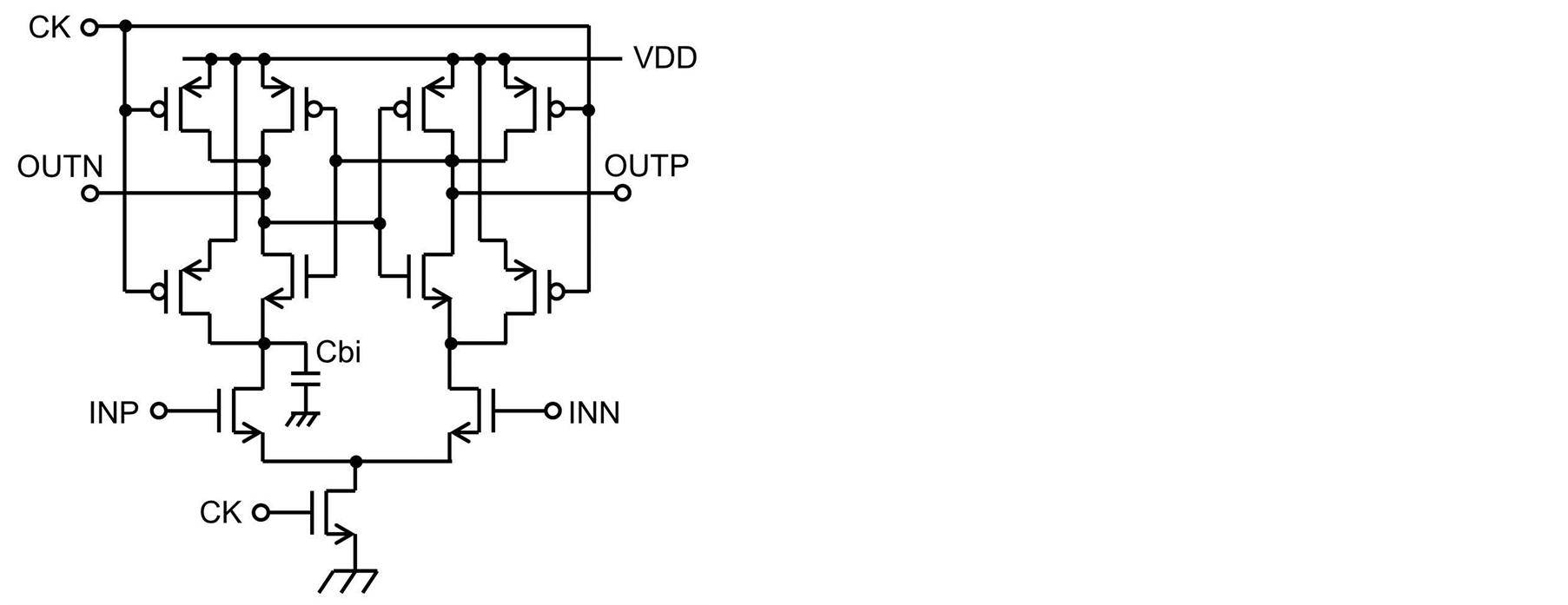
Figure 6. Schematic of built-in threshold circuit for FADC.
into the comparator. For example, the introduction of asymmetry of the load capacitance [14] and the current [17] were proposed. The introduction of asymmetry of the current is not suitable for high-precision ADCs because due to large amount of noise. The introduction of asymmetry of the load capacitor increases the delay time; however, these increase are negligible up to approximately 1 GHz. Therefore, this technique is commonly used in parallel ADCs.
A schematic of a comparator with the threshold voltage adjustment circuit is shown in Figure 7. The variable capacitors CcalP and CcalN are connected to the drain nodes of the input differential pair. The capacitance of the variable capacitor can be changed by the digital control signal (calibration code x). For example, CcalP is set to the minimum capacitance and CcalN is adjusted to an appropriate value when the threshold voltage of the INP side MOS transistor is higher than the nominal value. The minimum value of the variable capacitor is determined by the parasitic capacitance of the MOS transistor. The threshold voltage shift of the comparator can be expressed as
 , (3)
, (3)
where VOD is the overdrive voltage of the input differential pair and Cp is the minimum value of the variable capacitor. From Equation (3), the adjustment range of the threshold voltage is
 , (4)
, (4)
where Cmax is the maximum adjustment range of the variable capacitor, and ΔVth(max) can be increased by decreasing Cp/Cmax.
The MOS variable capacitor is commonly used, as shown in Figure 8. The PMOS transistors have binary weighted gate width and the gate capacitance changes according to the gate voltage. The minimum gate width is determined by the fabrication technology, for example, the minimum value is approximately 0.2 μm for 65-nm CMOS technology. The calculated capacitance of the variable capacitor and the threshold voltage of the comparator are also shown in Figure 8. The minimum capacitance is very large; more than 40 fF, because the MOS capacitor has parasitic capacitances of the overlapping capacitance and source/drain capacitances. On the contrary, Cmax is only 15 fF; therefore, Cp/Cmax is a large value of 3.1, resulting in a small threshold adjustment range of 20 mV. The power consumption in the case of maximum capacitance is also very large; 64 μW at the operating frequency of 1 GHz, due to large capacitance.
Another implementation of a variable capacitor is shown in Figure 9. This comprises metal oxide metal (MOM) capacitors and MOS switches. The capacitance can be changed by connecting and disconnecting the MOM capacitors using the MOS switches. A MOM capacitor has smaller parasitic capacitance compared with a MOS capacitor; therefore, Cp/Cmax can be reduced. The simulation results show that the capacitance increases as the calibration code like stairs; that is, the capacitance jumps every 16 codes. This is due to the parasitic capacitances of the MOS switches. The capacitance change is shown in Figure 10 when the calibration code changes from 15 to 16. The MOM capacitors are connected to GND when the MOS switches are on. However, the

Figure 7. Schematic of a comparator with the threshold voltage adjustment circuit.

Figure 8. MOS variable capacitor.

Figure 9. Variable capacitor comprised of MOM capacitors and MOS switches.

Figure 10. Capacitance change in variable capacitor.
overlapping capacitance (Cov) and drain-body capacitance (Cdb) are connected to the MOM capacitors in serial when the MOS switches are off; therefore, the MOS capacitors cannot be disconnected completely. The parasitic capacitance (Cov + Cdb) is approximately 0.2 fF when the gate width of the MOS switch is 0.2 μm. For example, the capacitance decreases by only 30% in the case of smallest capacitance (0.1 fF) when the MOS switch is off because the parasitic capacitance is larger than the MOM capacitance. This causes a large jump in the total capacitance when the calibration code changes from 15 to 16, as shown in Figure 10. The large jump in the total capacitance causes a large threshold voltage change (3.5 mV in the case of Figure 10), resulting in low-precision calibration.
We propose the low-power and high-resolution threshold voltage adjustment technique, as shown in Figure 11. This variable capacitor comprises MOM capacitors and MOS switches. A relatively large MOM capacitance (2.1 fF) is selected to reduce the effect of the parasitic capacitance of the MOS switches. This enables the capacitance to decrease by 90% when the switch is off; however, larger MOM capacitance increases power dissipation. Therefore, scaling capacitors (4.1 fF and 17.4 fF) are introduced in serial. Scaling capacitors effectively reduce the total capacitance; therefore, a variable range of 3.7 to 8.7 fF can be achieved, resulting in small Cp/Cmax of 0.7. The threshold adjustment range is 40 mV and the maximum threshold jump is 1.0 mV. The power dissipation is only 19 μW when the variable capacitance is maximum value.
4.3. Offset Drift Compensation Technique
One of the issues in putting foreground calibration to practical use is the offset drift due to temperature change. Foreground calibration measures the offset at a certain temperature and compensates for it; therefore, the offset cannot be perfectly compensated when the temperature changes after calibration because the offset changes depending on the temperature. We analyze the mechanism of offset drift using a simple model and propose a drift compensation technique. The analysis model of the offset drift is shown in Figure 12. The offset in a comparator is approximately determined by the mismatch of the differential pair; therefore, we developed an offset drift model focusing on the differential pair. The various mismatches in the differential pair cause offset voltage. We consider the mismatch of the threshold voltage and transistor size. The offset voltage can be expressed as
 , (5)
, (5)
where Vcom is the input common level. The first term is the mismatch of the threshold voltage, which mainly occurs due to the variability of the channel dopant concentration. The second term is due to the variability of the channel size. The offset drift can be obtained by differentiating this equation with respect to temperature.
 (6)
(6)
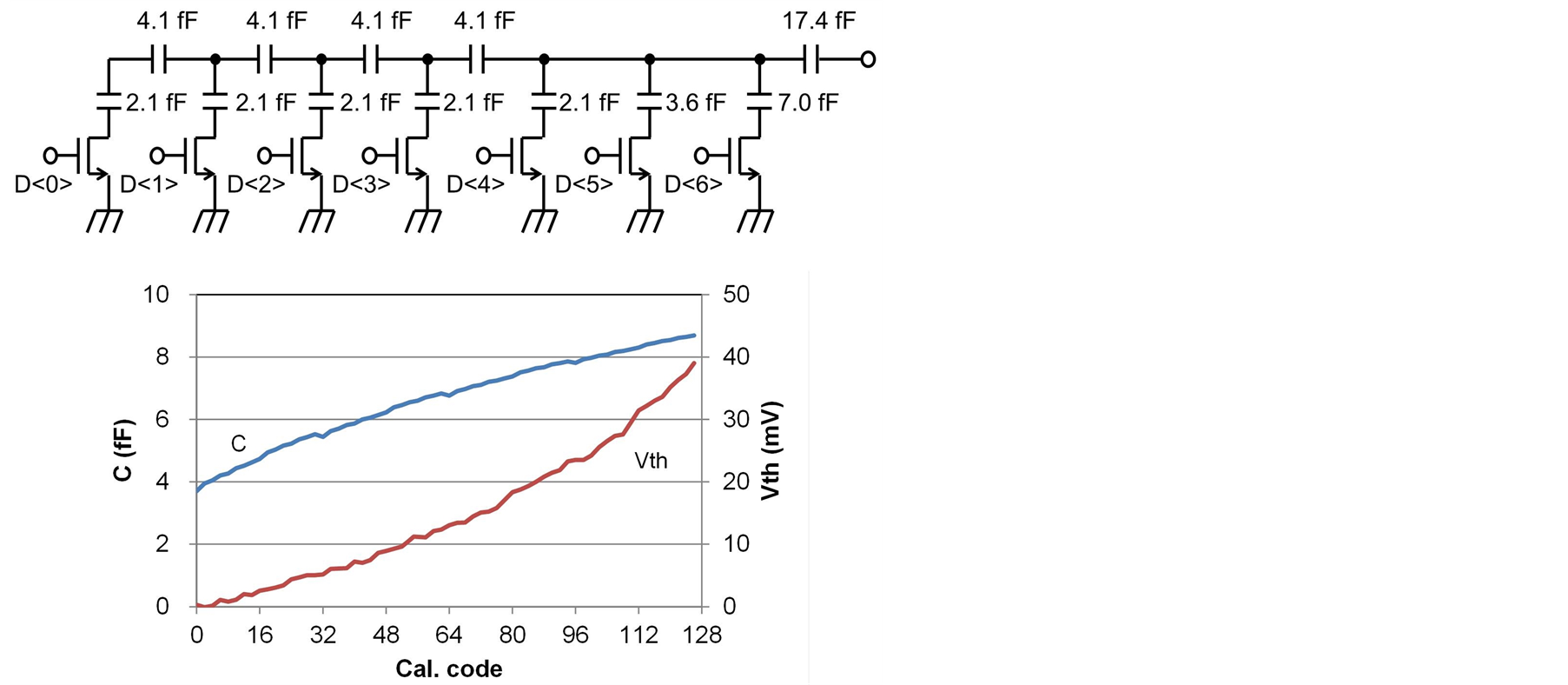
Figure 11. Proposed variable capacitor.
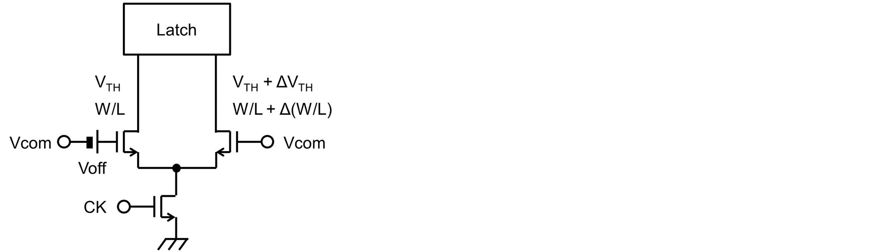
Figure 12. Offset drift model.
The first and second terms fluctuate without correlation because their physical factors of variability are completely different. Therefore, the offset drifts of two comparators are different even when they have the same initial offset voltage because the breakdown of the offsets (the amount of the first and second terms) is different. Therefore, the offset drift compensation on the basis of the initial offset fails. However, the offset drift can be reduced if dVcom/dT equals dVTH/dT because this condition nullifies the second term. Figure 13 shows the dVcom/dT dependence of the offset variation. Calibration was done at 25˚C, then the temperature was raised to 85˚C and the offset change was simulated. The offset voltage immediately after calibration was 0.29 mV. The offset voltage at 85˚C increased by 0.8 mV when dVcom/dT = 0. The offset voltage change, however, could be suppressed to 0.1 mV when dVcom/dT = −0.6 mV/˚C.
5. Post-Layout Simulation Results
The proposed ADC has been designed in a 65-nm digital CMOS technology. Figure 14 shows a layout plot of the ADC. The CDAC is located between CADC and FADC to shorten the analog input signal line. The core area excluding the output buffer is 520 × 370 μm. The supply voltage is 0.8 V and power dissipation is 7 mW at a sampling frequency of 1 GHz. Figure 15 shows the simulated input frequency dependence of the signal-to-noise and distortion ratio (SNDR) and spurious-free dynamic range (SFDR). The simulation was conducted using the netlist extracted from the layout pattern. The SNDR and SFDR were approximately constant from 10 MHz to 1 GHz. Figure 16 shows the simulated sampling frequency dependence of the SNDR and SFDR. The SNDR dropped when the sampling frequency exceeded 1 GHz. The reason performance degraded over 1 GHz was the timing margin failure in the encoder. Figure 17 shows the simulation results of calibration. A large error occurred due to mismatch before calibration, resulting in a poor SNDR and SFDR of 23.7 and 35.5 dB, respectively. The calibration greatly improved the SNDR and SFDR to 45.5 and 53.8 dB, respectively. Table 1 summarizes the ADC performance and the recently developed ADCs in similar target specifications [4] [6] [20] [21] . Our ADC demonstrates the lowest FOM of 51 fJ/conv.-step in the subranging ADCs. The SAR ADC [20] exhibits very low FOM; however, good performance is possible using 32-nm CMOS technology.

Table 1. Performance comparison.

Figure 13. dVcom/dT dependence of the offset variation.
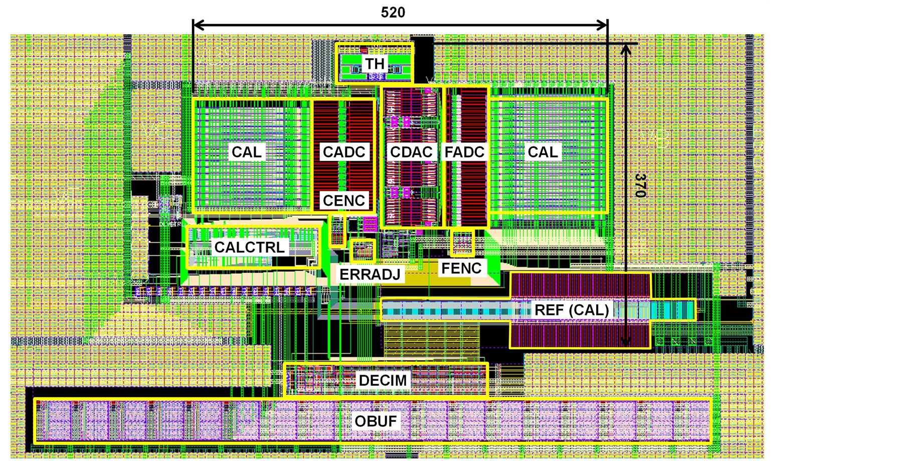
Figure 14. Layout plot of designed ADC.
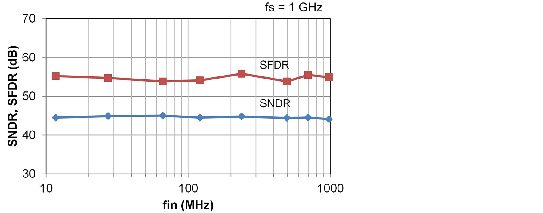
Figure 15. Simulated input frequency dependence of SNDR and SFDR.

Figure 16. Simulated sampling frequency dependence of SNDR and SFDR.
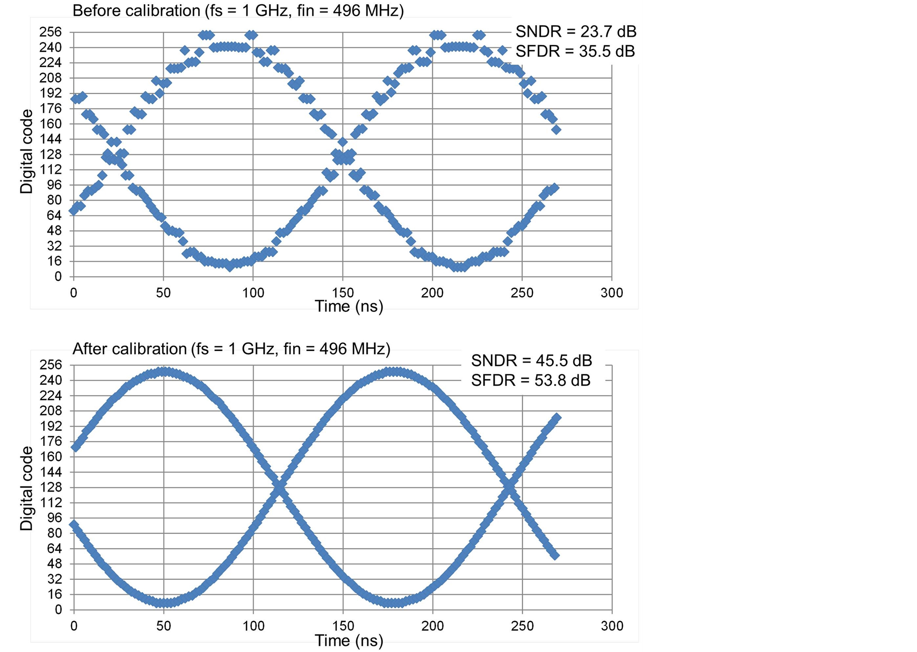
Figure 17. Simulation results of calibration.
6. Conclusion
We proposed an ADC architecture combining a capacitive DAC and a built-in threshold calibration to eliminate the resistor ladder, resulting in a low-power subranging ADC. We also proposed a variable capacitor using scaling capacitance to reduce power dissipation of the comparator and an offset drift compensation technique for high-precision foreground calibration. The designed ADC combining these techniques achieves a high sampling frequency of 1 GHz and low power dissipation of 7 mW, resulting in an FOM of 51 fJ/conv.-step.
Acknowledgements
The authors thank Nobuo Kano, Koichi Ono, Junichi Naka, and Osamu Kobayashi for their valuable discussions. This work was supported by the Semiconductor Technology Academic Research Center (STARC). It was also supported by the VLSI Design and Education Center (VDEC), the University of Tokyo with the collaboration of Cadence Design Systems, Inc. and Mentor Graphics, Inc.
References
- Yun-Shiang, S. (2012) A 6b 3GS/s 11 mW Fully Dynamic Flash ADC in 40 nm CMOS with Reduced Number of Comparators. 2012 Symposium on VLSI Circuits (VLSIC), 2012, 26-27.
- Nakajima, Y., Kato, N., Sakaguchi, A., Ohkido, T., Shimomaki, K., Masuda, H., et al. (2012) A 7b 1.4GS/s ADC with Offset Drift Suppression Techniques for One-Time Calibration. 2012 IEEE Custom Integrated Circuits Conference (CICC), 2012, 1-4.
- Jong-In, K., Wan, K., Barosaim, S. and Seung-Tak, R. (2011) A Time-Domain Latch Interpolation Technique for Low Power Flash ADCs. 2011 IEEE Custom Integrated Circuits Conference (CICC), 2011, 1-4.
- Ohhata, K., Takase, H., Tateno, M., Arita, M., Imakake, N. and Yonemitsu, Y. (2012) A 1-GHz, 17.5-mW, 8-Bit Subranging ADC Using Offset-Cancelling Charge-Steering Amplifier. 2012 IEEE Asian Solid State Circuits Conference (A-SSCC), 2012, 149-152.
- Ku, I.N., Xu, Z., Yen-Cheng, K., Yen-Hsiang, W. and Chang, M.C.F. (2011) A 40-mW 7-Bit 2.2-GS/s Time-Interleaved Subranging ADC for Low-Power Gigabit Wireless Communications in 65-nm CMOS. 2011 IEEE Custom Integrated Circuits Conference (CICC), 2011, 1-4.
- Yung-Hui, C. and Jieh-Tsorng, W. (2011) A 16-mW 8-Bit 1-GS/s Subranging ADC in 55nm CMOS. 2011 Symposium on VLSI Circuits (VLSIC), 2011, 128-129.
- Ohhata, K., Uchino, K., Shimizu, Y., Oyama, Y. and Yamashita, K. (2008) A 770-MHz, 70-mW, 8-Bit Subranging ADC Using Reference Voltage Precharging Architecture. Solid-State Circuits Conference, 2008. A-SSCC’08. IEEE Asian, 2008, 41-44.
- Yuan-Ching, L. (2012) A 4.5-mW 8-b 750-MS/s 2-b/Step Asynchronous Subranged SAR ADC in 28-nm CMOS Technology. 2012 Symposium on VLSI Circuits (VLSIC), 2012, 88-89.
- Chi-Hang, C., Yan, Z., Sai-Weng, S., Seng-Pan, U. and Martins, R.P. (2012) A 3.8 mW 8b 1GS/s 2b/Cycle Interleaving SAR ADC with Compact DAC Structure. 2012 Symposium on VLSI Circuits (VLSIC), 2012, 86-87.
- Stepanovic, D. and Nikolic, B. (2012) A 2.8 GS/s 44.6 mW Time-Interleaved ADC Achieving 50.9 dB SNDR and 3 dB Effective Resolution Bandwidth of 1.5 GHz in 65 nm CMOS. 2012 Symposium on VLSI Circuits (VLSIC), 2012, 84-85.
- Doris, K., Janssen, E., Nani, C., Zanikopoulos, A. and Van Der Weide, G. (2011) A 480 mW 2.6 GS/s 10b 65 nm CMOS Time-Interleaved ADC with 48.5 dB SNDR up to Nyquist. 2011 IEEE International Solid-State Circuits Conference Digest of Technical Papers (ISSCC), 2011, 180-182.
- Zhiheng, C. and Shouli, Y. (2008) A 52 mW 10b 210 MS/s Two-Step ADC for Digital-IF Receivers in 0.13- BC;m CMOS. Custom Integrated Circuits Conference, 2008. CICC 2008. IEEE, 2008, 309-312.
- Asada, Y., Yoshihara, K., Urano, T., Miyahara, M. and Matsuzawa, A. (2009) A 6 Bit, 7 mW, 250 fJ, 700 MS/s Subranging ADC. Solid-State Circuits Conference, 2009. A-SSCC 2009. IEEE Asian, 2009, 141-144.
- Van der Plas, G., Decoutere, S. and Donnay, S. (2006) A 0.16 pJ/Conversion-Step 2.5 mW 1.25 GS/s 4b ADC in a 90 nm Digital CMOS Process. Solid-State Circuits Conference, 2006. ISSCC 2006. Digest of Technical Papers. IEEE International, 2006, 2310.
- Tsugaru, K., Sugimoto, Y., Noda, M., Iwai, H., Sasaki, G. and Suwa, Y. (1989) A 10 bit 40 MHz ADC Using 0.8 μm Bi-CMOS Technology. Bipolar Circuits and Technology Meeting, 1989, Proceedings of the 1989, 1989, 48- 51.
- Lee, H., Asada, Y., Miyahara, M. and Matsuzawa, A. (2013) A 6 Bit, 7 mW, 700 MS/s Subranging ADC Using CDAC and Gate-Weighted Interpolation. IEICE Transaction on Fundamentals, E96-A, 422-433.
- Figueiredo, P.M., Cardoso, P., Lopes, A., Fachada, C., Hamanishi, N., Tanabe, K., et al. (2006) A 90 nm CMOS 1.2v 6b 1GS/s Two-Step Subranging ADC. Solid-State Circuits Conference, 2006. ISSCC 2006. Digest of Technical Papers. IEEE International, 2006, 2320-2329.
- Jong-In, K., Ba-Ro-Saim, S., Wan, K. and Seung-Tak, R. (2013) A 6-b 4.1-GS/s Flash ADC with Time-Domain Latch Interpolation in 90-nm CMOS. IEEE Journal of Solid-State Circuits, 48, 1429-1441.
- Paik, D., Miyahara, M. and Matsuzawa, A. (2012) An Analysis on a Dynamic Amplifier and Calibration Methods for a Pseudo-Differential Dynamic Comparator. IEICE Transactions on Fundamentals of Electronics, Communications and Computer Sciences, E95-A, 456-470.
- Kull, L., Toifl, T., Schmatz, M., Francese, P.A., Menolfi, C., Braendli, M., et al. (2013) A 3.1 mW 8b 1.2 GS/s SingleChannel Asynchronous SAR ADC with Alternate Comparators for Enhanced Speed in 32 nm Digital SOI CMOS. 2013 IEEE International Solid-State Circuits Conference Digest of Technical Papers (ISSCC), 2013, 468-469.
NOTES
*Corresponding author.