Circuits and Systems
Vol.5 No.1(2014), Article ID:41935,6 pages DOI:10.4236/cs.2014.51002
Design of Low Power Comparator Using DG Gate
1Young Researchers and Elite Club, Sarvestan Branch, Islamic Azad University, Sarvestan, Iran
2Department of Electrical Engineering, Zarghan Branch, Islamic Azad University, Zarghan, Iran3Department of Electrical Engineering, Sarvestan Branch, Islamic Azad University, Sarvestan, IranEmail: *Bahramdehghan1@gmail.com
Copyright © 2014 Bahram Dehghan et al. This is an open access article distributed under the Creative Commons Attribution License, which permits unrestricted use, distribution, and reproduction in any medium, provided the original work is properly cited. In accordance of the Creative Commons Attribution License all Copyrights © 2014 are reserved for SCIRP and the owner of the intellectual property Bahram Dehghan et al. All Copyright © 2014 are guarded by law and by SCIRP as a guardian.
Received November 18, 2013; revised December 18, 2013; accepted December 25, 2013
Keywords: Reversible Logic Comparator; TR and DG Gate; Quantum Cost; Garbage Output
ABSTRACT
In recent studies, reversible logic has emerged as a great scene of research, having applications in low power CMOS circuits, optical computing, quantum computing and nanotechnology. The classical logic gates such as AND, OR, EXOR and EXNOR are not reversible. In the existing literature, reversible sequential circuits designs are offered that are improved for the number of the garbage outputs and reversible gates. Minimizing the number of garbage is very noticeable. In the present paper, we show a design of the reversible comparator based on the quantum gates implementation of the reversible DG gate. The reversible DG gate is designed by using 3 × 3 quantum gates such as NOT, CNOT, Controlled-V and Controlled-V+ gates. Also, we have used the TR gate and various types of quantum gates in the implementation results. Low power three-bit comparator is designed using DG Gate, New Gate and Fredkin Gate. In order to evaluate the benefit of using the DG gate proposed in this paper, one-bit comparator is constructed. The design is useful for the future computing techniques like quantum computers. The proposed designs are implemented using VHDL and functionally investigated using Quartus II simulator.
1. Introduction
Conventional combinational logic circuits dissipate heat for every bit of information that is lost during their operation [1]. According to Landauer’s principle, each bit of data lost produces kTln2 joules amount of heat, where k is Boltzmann’s constant and T is the absolute temperature at which the operation is implemented [2]. Moore’s law [3] previses exponential growth of the heat generated due to the information loss, which will be a significant amount of heat loss in the next decade.
Bennett [4] illustrated that zero energy dissipation would be possible only if the network based on reversible gates. Hence, reversibility will become a necessary property in future circuit design.
There are two Boolean constants, 0 and 1. Reversible circuits are those circuits that do not lose information.
These circuits can produce single output vector from each input vector, and conversely, there was a one-to-one mapping between output and input vectors. Hence, an N × N reversible gate can be represented as:
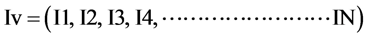
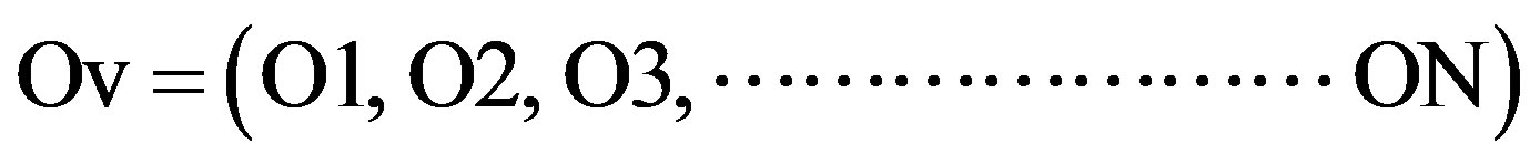
where Iv and Ov can be shown the input and output vectors respectively; the significant cost metrics in the synthesis of reversible logic circuits are the number of garbage outputs, delay and quantum cost [5,6]. Any unitary operation must be reversible. Thus, quantum networks effecting primary arithmetic operations such as addition, multiplication and exponentiation cannot be directly infered from their classical Boolean counterparts (classical logic gates such as AND or OR or EXOR are irreversible). Therefore, Quantum Arithmetic must be made from reversible logic combinations [7]. Various gates have been proposed over the last decades. Among them are the controlled-not (CNOT) introduced by Feynman [8] Toffoli [9], and Fredkin [10] gates. Digital Comparator is a combinational circuit that compares two inputs binary quantities (A and B) and produces outputs to indicate whether the inputs are equal or which input is greater than the other. Therefore, the circuit has three outputs to indicate whether A = B, A > B or A < B.
In this paper, we present various designs of a three-bit comparator circuit using existing reversible logic gates. The present paper proposed a new gate, called reversible DG gate which was used in the design of comparator. All the comparators have been modeled and investigated using VHDL and Quartus II.
2. Basic Reversible Gates
The detailed cost of a reversible gate associates with any specific realization of quantum logic. A short description of the gates are given below.
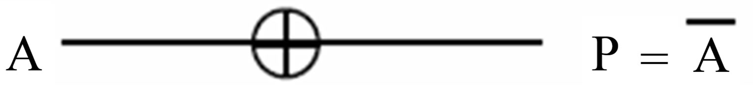
A. The NOT Gate A NOT gate is a 1 × 1 gate performed as shown in Figure 1(a). It has quantum cost of 1.
B. The Controlled-V and Controlled-V+ Gates The Quantum cost of a Reversible gate is computed by counting the number of V, V+ and CNOT gates [11]. The controlled-V and V+ gates are shown in Figures 1(b) and (c).
The Controlled-V and Controlled-V+ quantum gates have some properties that are shown below:
 (a)
(a)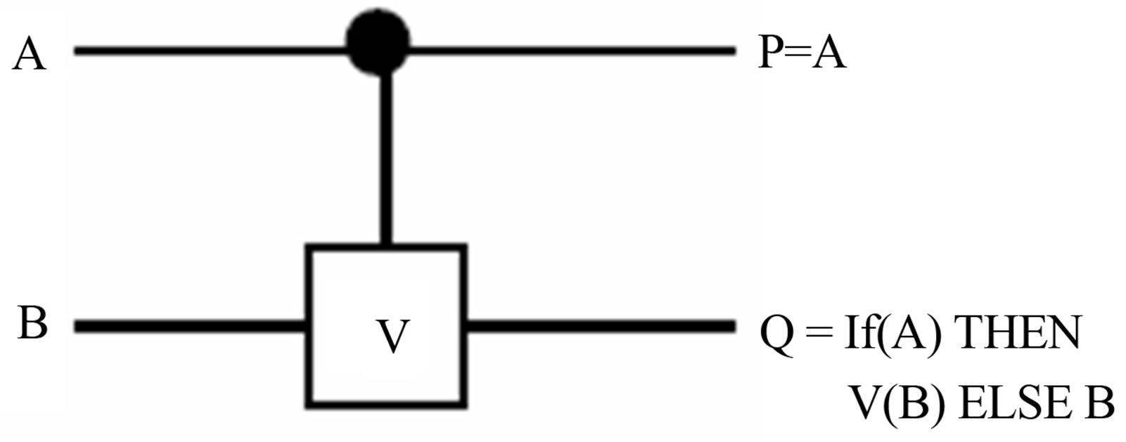 (b)
(b)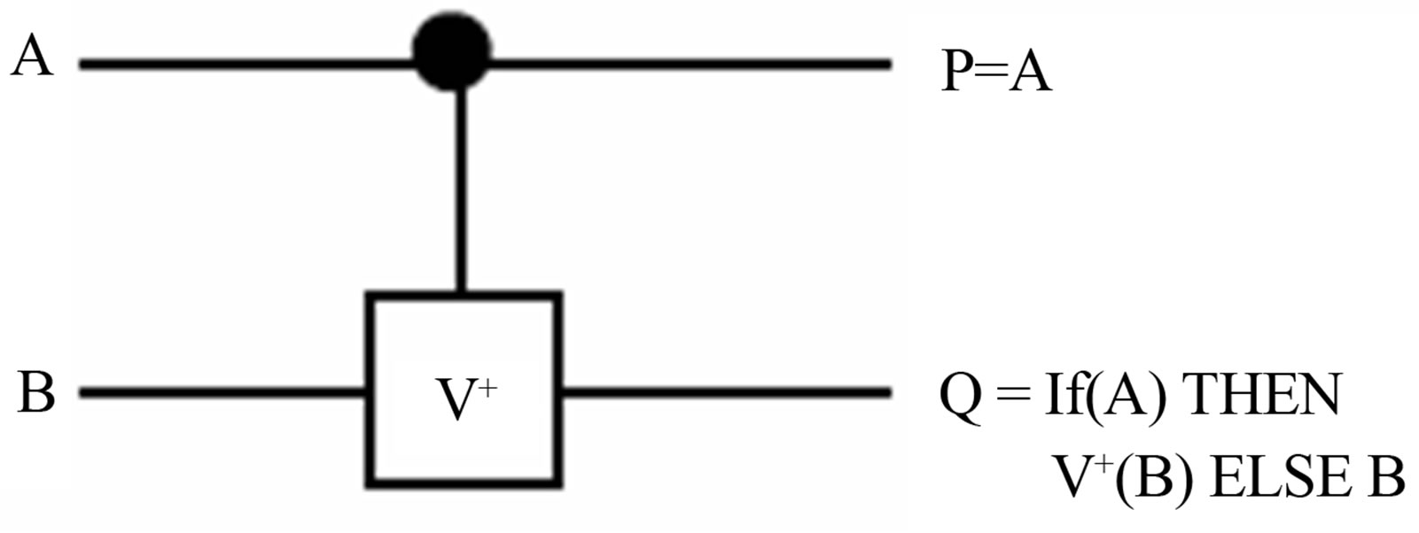 (c)
(c)
Figure 1. a) Not gate; b) Controlled-V gate; c) ControlledV+ gate.
These equations depict that two V or V+ gates in series are equivalent to a NOT gate; and two V and V+ in series, are equivalent a BUFFER gate.
C. Feynman Gate The most popular (2, 2) one-through reversible gate is the Feynman gate [8]. The logical functions performed by a Feynman gate with input vector (A, B) and output vector (P, Q) are represented in Figure 2.
The input double (A, B) depends on its output double (P, Q) as follows.
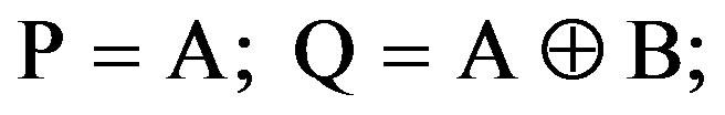
If A = 0 then Q would be equal to B. If A = 1 then showed the complement of the input (B).
Hence, it is called as quantum XOR and also called as CNOT (1-NOT).
D. Fredkin gate Fredkin gate [10], depicted in Figure 3, is a (3, 3) reversible gate which penetrates P = A, Q = A'B ⊕ AC and R = A'C ⊕ AB where (A, B, C) is the input vector and (P, Q, R) is the output vector.
Figures 4(a) and (b) offer the performance of the Fredkin gate as AND and OR functions respectively.
E. New gate The New gate [12] is a (3, 3) reversible gate. The most significant aspect of this gate is that it can work as a universal gate.
Figure 2. Feynman gate.
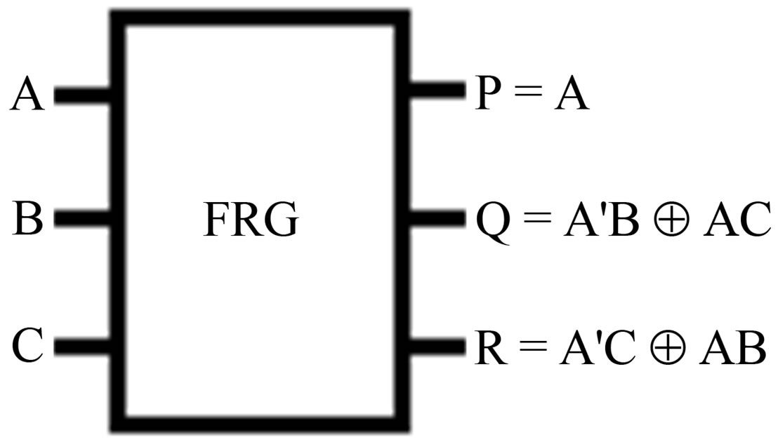
Figure 3. Fredkin gate.
 (a)
(a)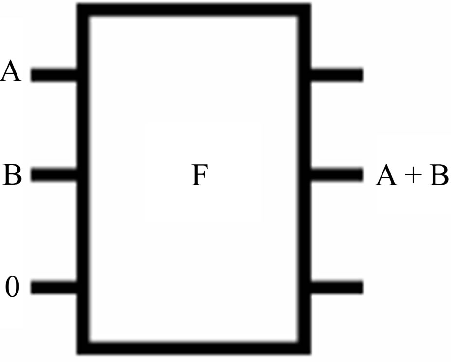 (b)
(b)
Figure 4. Fredkin gate as a) AND function; b) OR function.
The New gate is one of the most popular reversible as represented in Figure 5.
F. BVF gate This is a (4, 4) reversible logic gate [13] shown in Figure 6 with input vector I (A, B, C, D) and the output vector is O (P, Q, R, S) . This can be used for duplication of the required inputs to meet the fan-out requirements. This gate can be specified by P = A, Q = A ⊕ B, R = C and S = C ⊕ D.
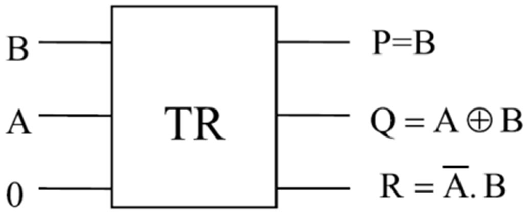
G. TR gate Recently Thapliyal and Ranganathan in [14] have proposed a new design of the reversible full subtractor based on the offered quantum gates implementation of the TR gate. TR gate with quantum cost of 4. The quantum cost of TR gate is 4 since it requires 1 V+ gates, 2 V gate and 1 CNOT gate in its structure.
TR gate and Quantum implementation of TR gate have represented in Figures 7(a) and (b) respectively.
3. Proposed Gate
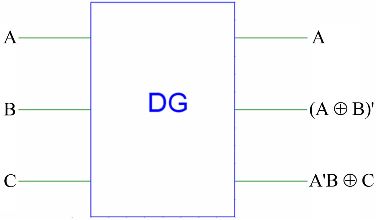
This paper presents a new (3, 3) reversible gate, “DG”,
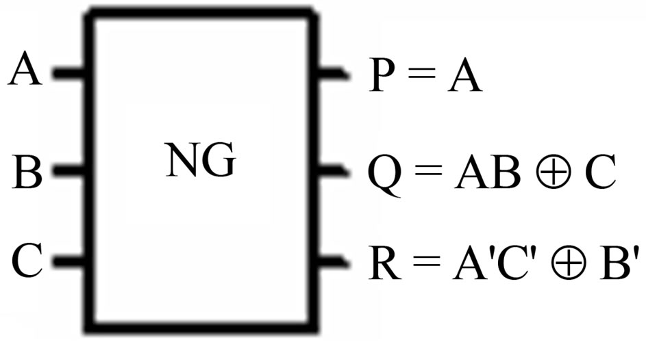
Figure 5. New gate.
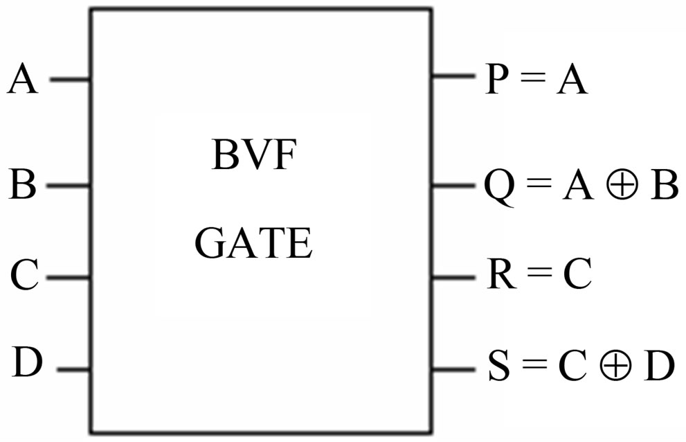
Figure 6. BVF gate [13].
 (a)
(a)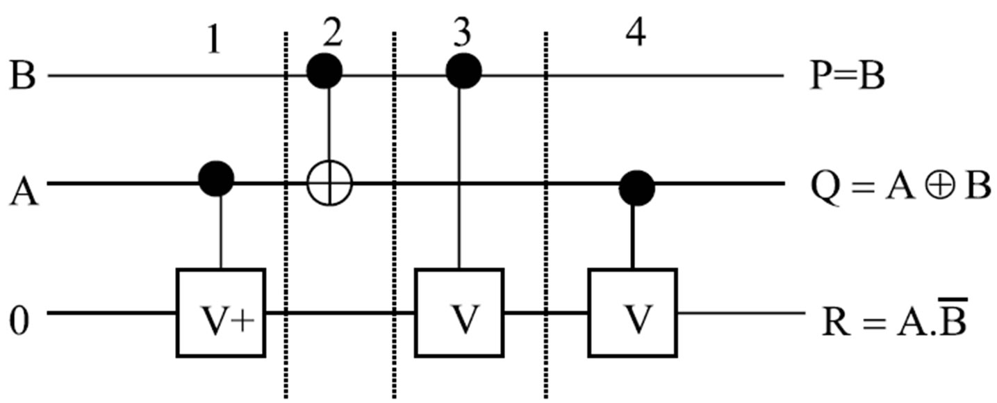 (b)
(b)
Figure 7. a) TR gate as a reversible half subtractor; b) Quantum implementation of TR gate based reversible half subtractor.
with inputs (A, B, C) and outputs P = A, Q = (A ⊕ B)', R = AB' ⊕ C that is shown in Figure 8(a). The gate is one-through, which means one of the input variables is also output. The corresponding truth table of DG gate is shown in Table 1. Figure 8(b) shows the quantum implementation of the DG with quantum cost of 5. The corresponding truth table of the DG gate is shown in Table 1.
4. Design of the Three Bit Comparator
The two numbers are equal if all pairs of significant digits are equal; meaning A3 = B3 and A2 = B2 and A1 = B1.
To check for this equality, we use the XNOR gate as we did previously.
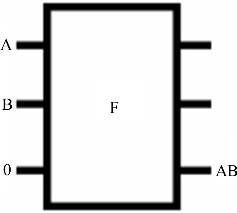
So we have seen three bit comparator (A = B) using classical gates as shown in Figure 9.
In the same way, the following classical gate A > B can be considered for a three bit comparator which is shown in Figure 10.
 (a)
(a)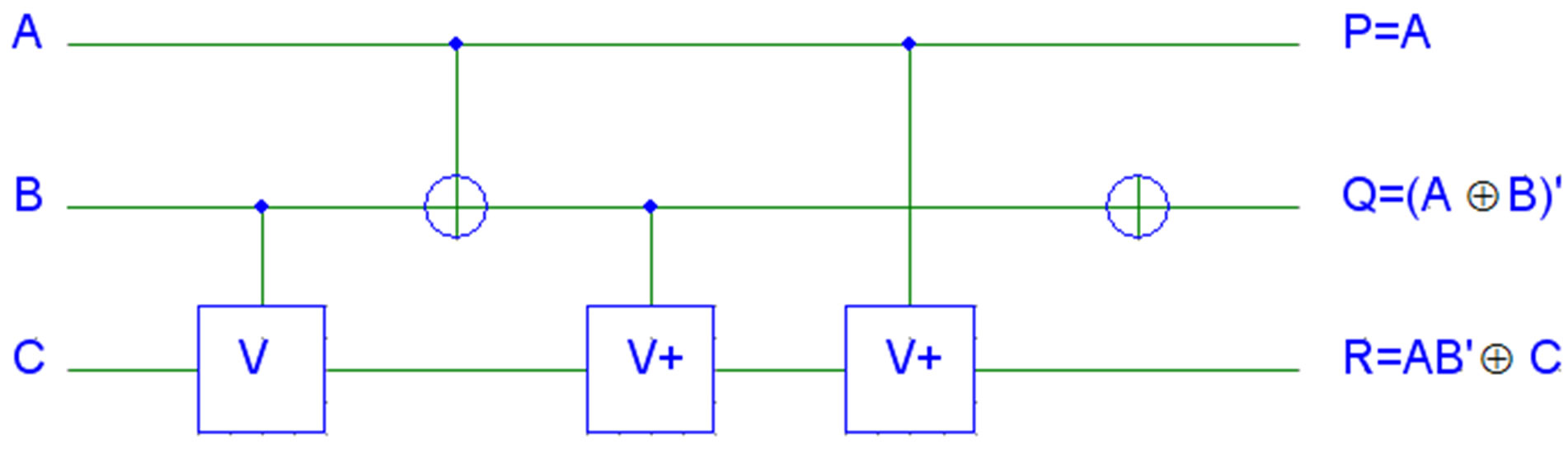 (b)
(b)
Figure 8. a) DG gate; b) Quantum implementation of DG gate.
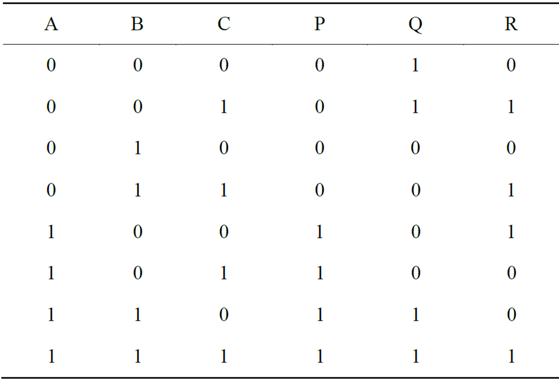
Table 1. Truth table for the DG gate.
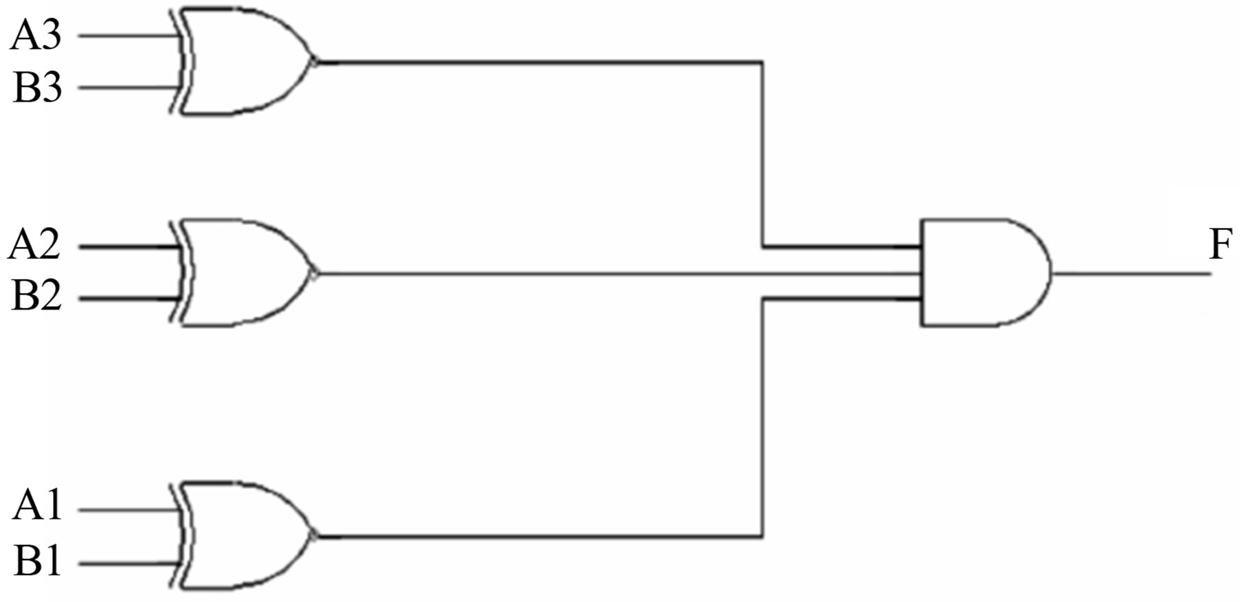
Figure 9. Three bit comparator (A = B) using classical gates.
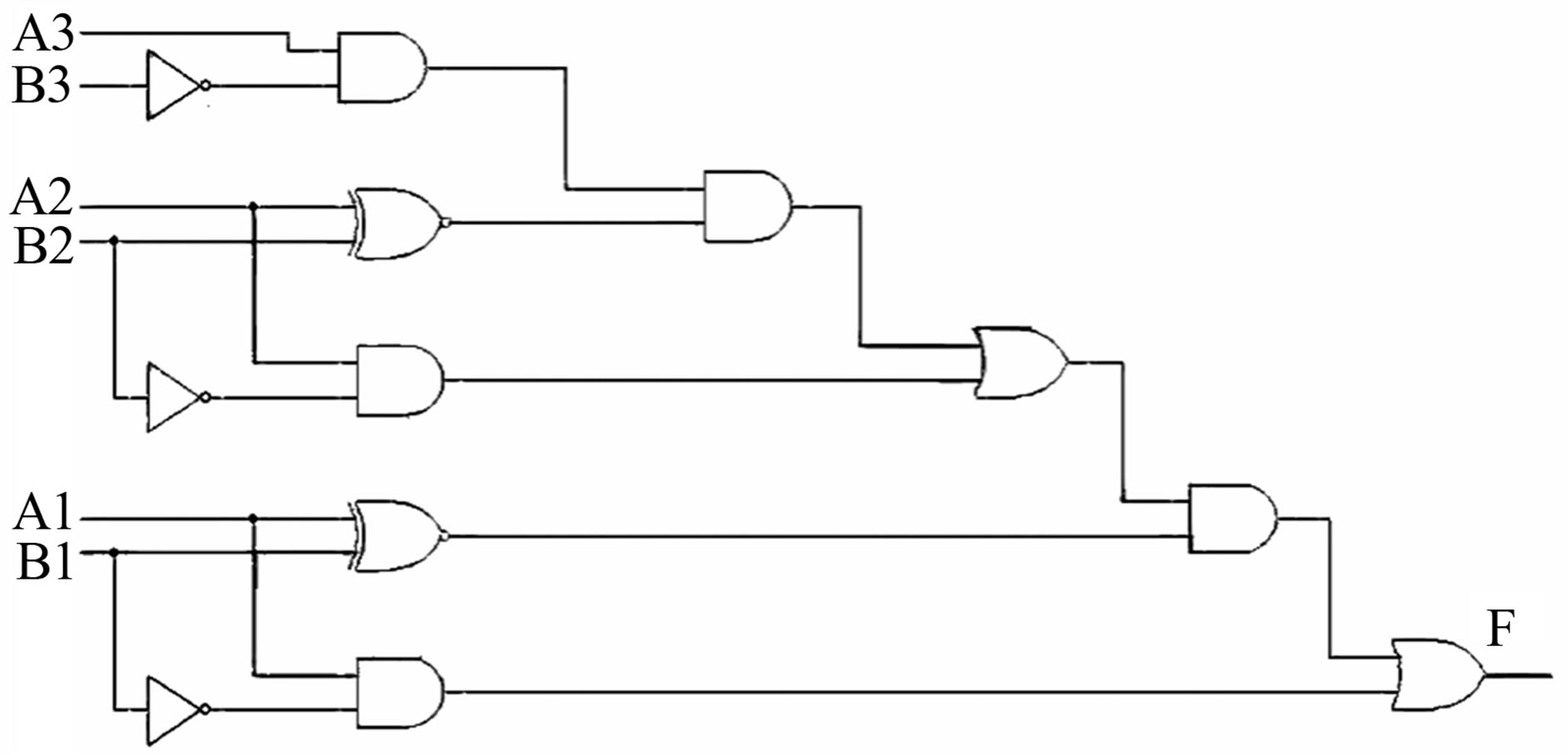
Figure 10. Three bit comparator (A > B) using classical gates.
If we want to have the output A = B, DG and BVF Gates can be used. The results are shown in Figure 11. Table 2 shows the evaluation of the mentioned circuit.
Two DG Gates can be put instead of BVF Gate to reduce the number of gates. The results are shown in Figure 12. Table 3 shows the evaluation of the mentioned circuit.
Reversible three bit comparator is implemented with various types of reversible logic gates as shown in Figures 13 and 14 respectively.
The proposed circuit of the three bit comparator is evaluated in terms of number of reversible gates used and garbage outputs generated. Tables 4 and 5 show the evaluation of the proposed circuits.
The results show that DG gate reduces the number of gates and garbage outputs.
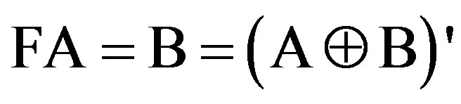
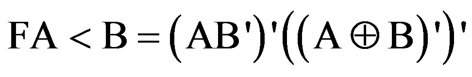
In the proposed one-bit comparator design, we have investigated FA > B and FA = B and the third condition FA < B is produced from the first two outputs. Therefore the design recitation leads to

The results are shown in Figure 15. DG gate is used in Figure 15 where DG and NG are used in Figure 10.
Figure 16 has less garbage outputs but in Figure 15, there are EXOR and EXNOR gates in outputs concur-
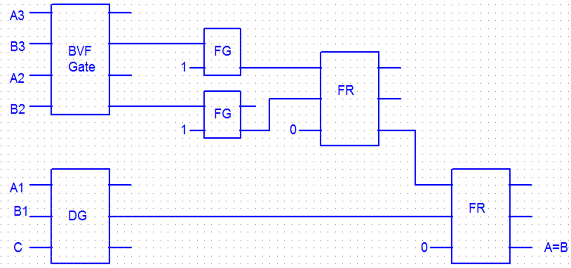
Figure 11. One bit (A = B) using BVF, DG Gates.
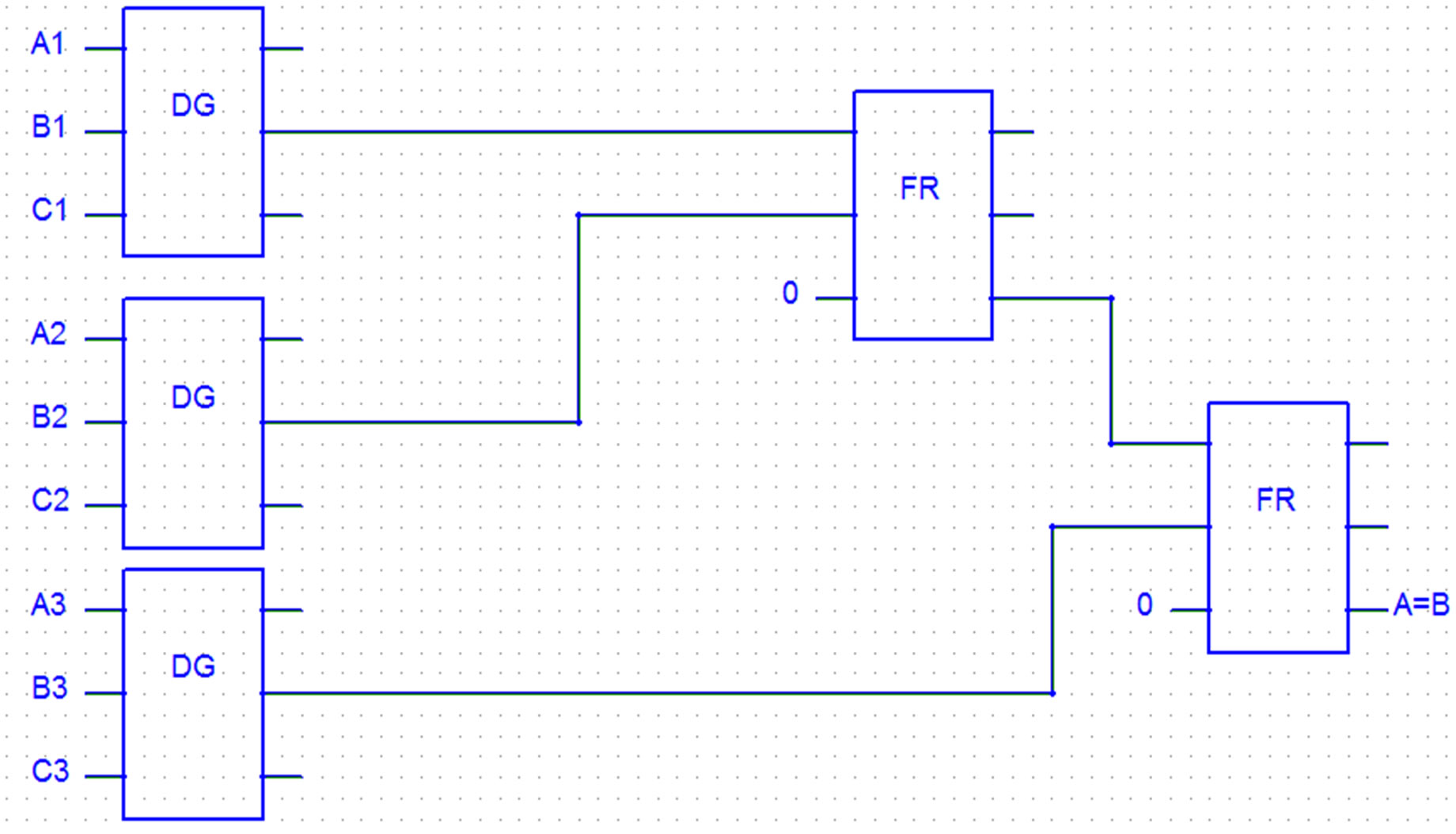
Figure 12. One bit (A = B) using DG gate.
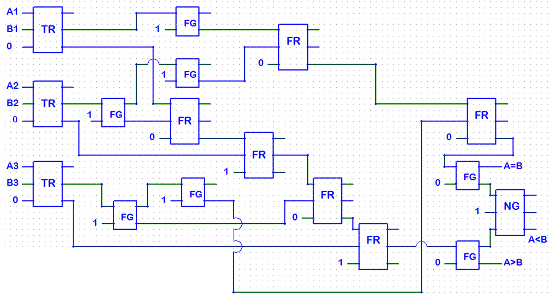
Figure 13. Three bit comparator using TR gate.
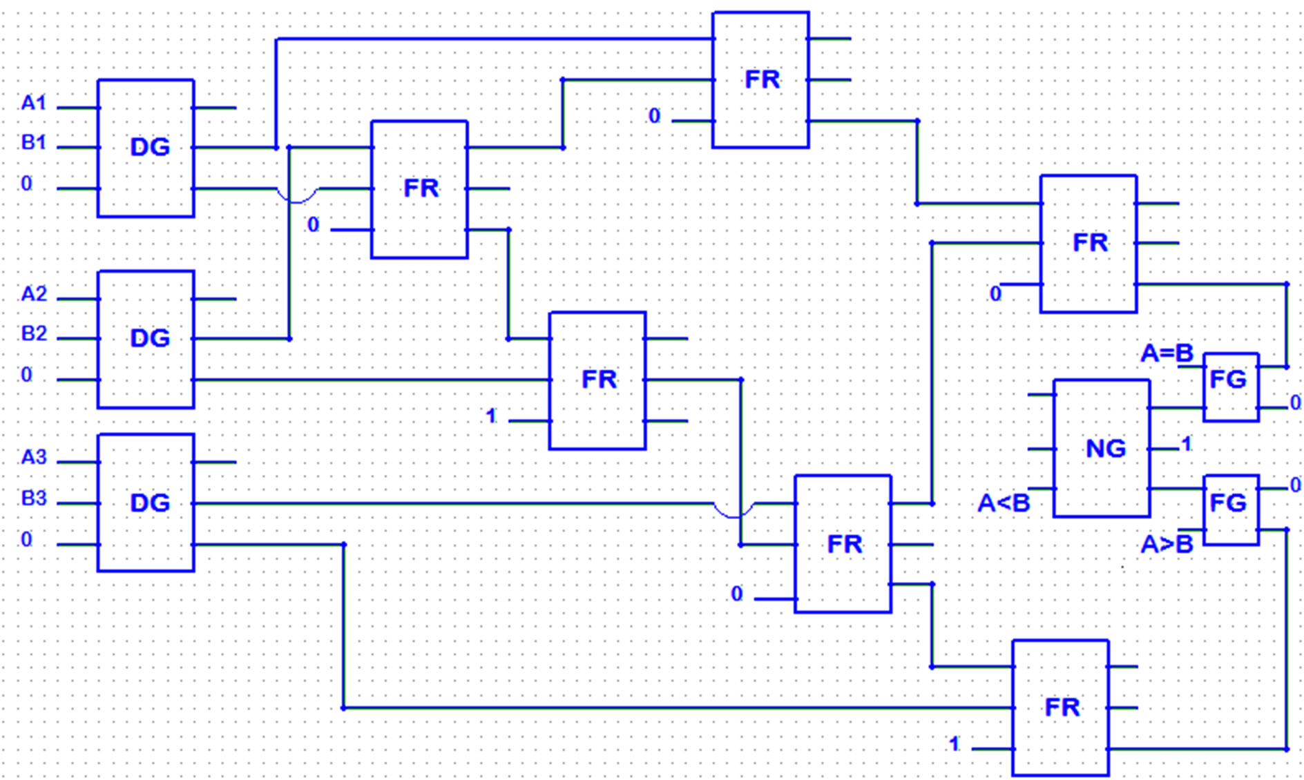
Figure 14. Three bit comparator using DG gate.
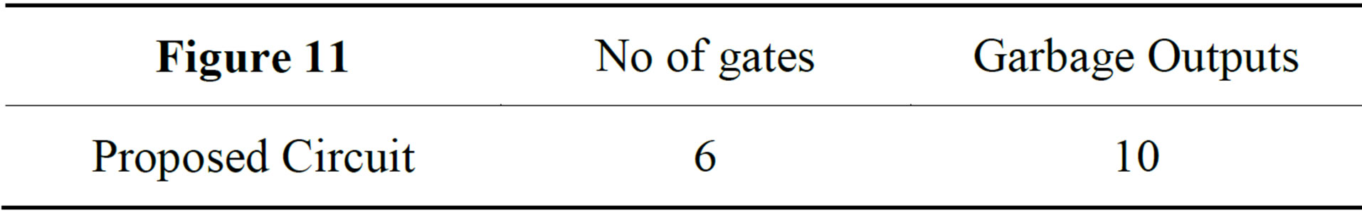
Table 2. Evaluation of the proposed comparator.
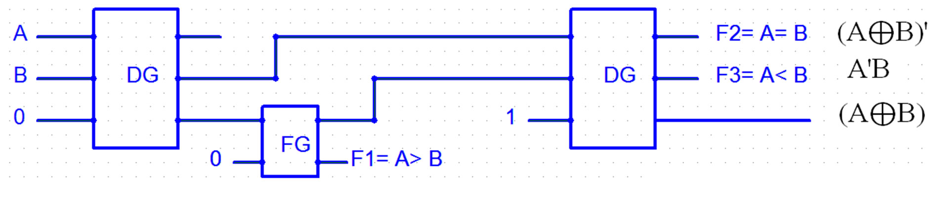
Figure 15. One bit comparator using DG gate.

Figure 16. One bit comparator using DG gate and NEW gate.
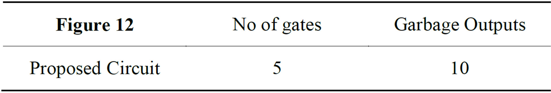
Table 3. Evaluation of the proposed comparator.
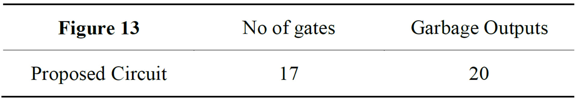
Table 4. Evaluation of the proposed comparator.
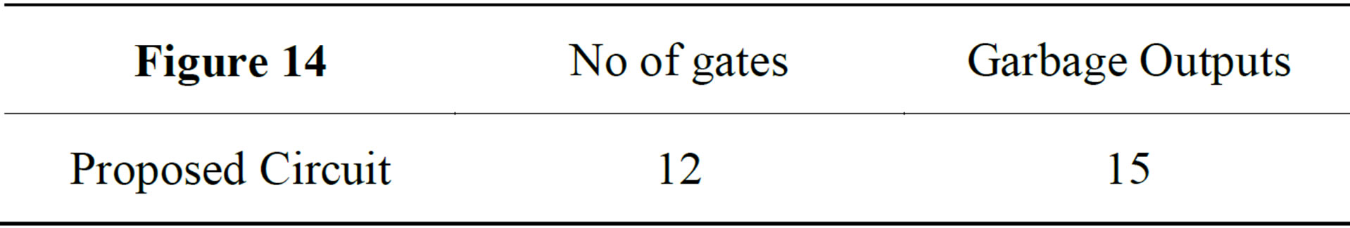
Table 5. Evaluation of the proposed comparator.
rently. Tables 6 and 7 show the evaluation of the proposed circuits.
In the mentioned paper one bit comparator has better function in comparison with Nagamani et al. Figure 17 is selected as follows, in Nagamani et al.
A good synthesis for reversible logic should not create an excessive “garbage” or “waste of outputs”. Hence, the components are chosen so that the designed scheme has the desired characteristics. One bit comparator can be represented by 2 DG gates and 1 FG gate, as shown in Figure 18. This structure can be utilized for testing outputs 1 and 3 (AB'). DG gate operates as a signal copying that shown in Figure 18. The corresponding table of mentioned circuit is shown in Table 8. The (A'B) output of the Figure 18 is given by the equation:
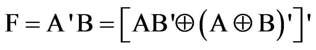
Figure 18 has better performance because of similarity gates and two same outputs. Although garbage outputs seems zero. Table 8 shows the evaluation of the mentioned circuit.
Two same outputs of this Figure can be used for concurrent error detection.
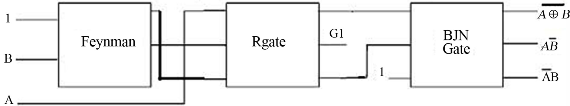
Figure 17. One bit comparator using R gate and BJN gate [1].
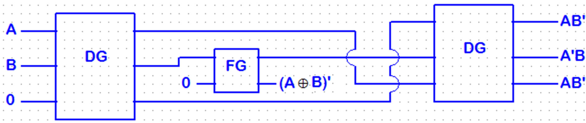
Figure 18. One bit comparator using DG gate.
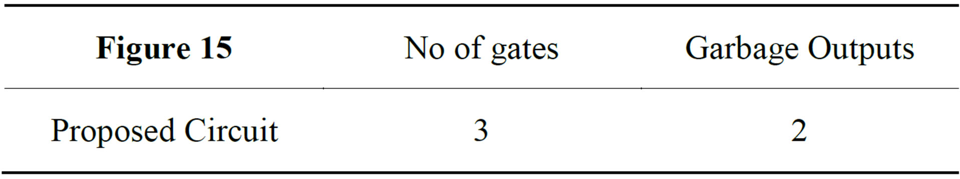
Table 6. Evaluation of the proposed comparator.
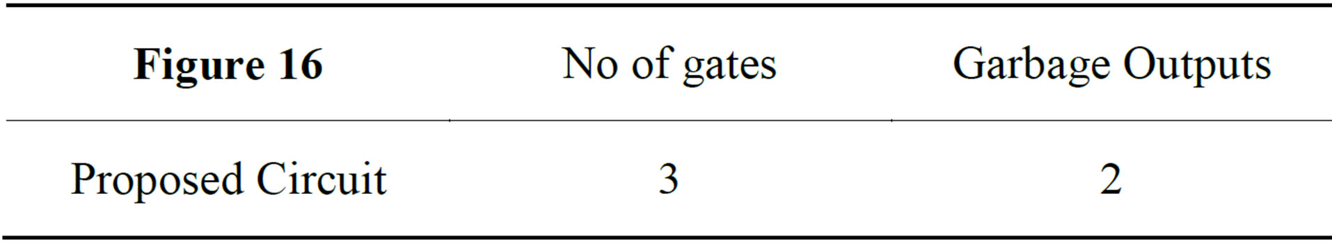
Table 7. Evaluation of the proposed comparator.
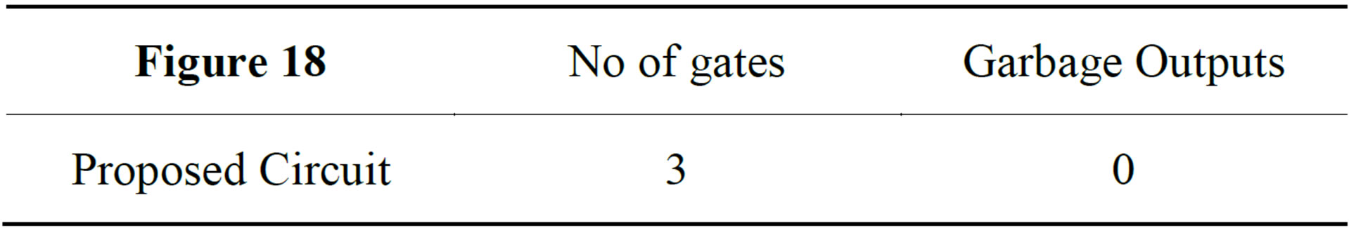
Table 8. Evaluation of the proposed comparator.
5. Simulation Results
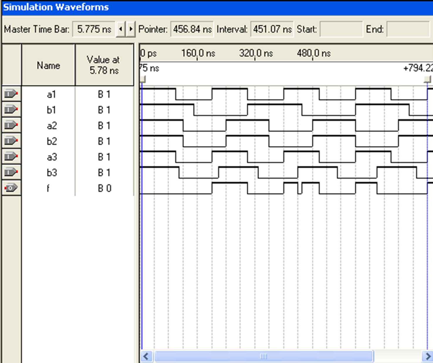
Reversible logic gates are extensively known to be compatible with future computing technologies which approximately dissipate zero heat [15]. For example, Reversible three bit comparators offered using VHDL and Simulated using Quartus II Simulator. Simulation results are shown in Figures 19(a) and (b). For one bit comparator using DG gate result shown in Figure 19(c).
6. Discussions and Conclusions
Conventional computers generate heat and waste much energy. In order to make a computer faster and lower power, consumption proposed reversible logic gates. In this paper, we have presented new designs of reversible one and three-bit comparators based on the quantum gates implementation of the reversible TR and DG. The main goal of this paper is optimized in terms of number of garbage outputs, gate count and quantum cost for comparator designs. The proposed DG gate can be combined with TR gate and various types of reversible logic gates to design minimal quantum cost and garbage less reversible circuits.
The newly proposed DG gate can be used for imple-
 (a)
(a) 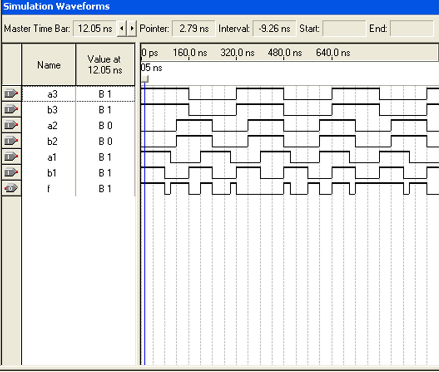 (b)
(b) 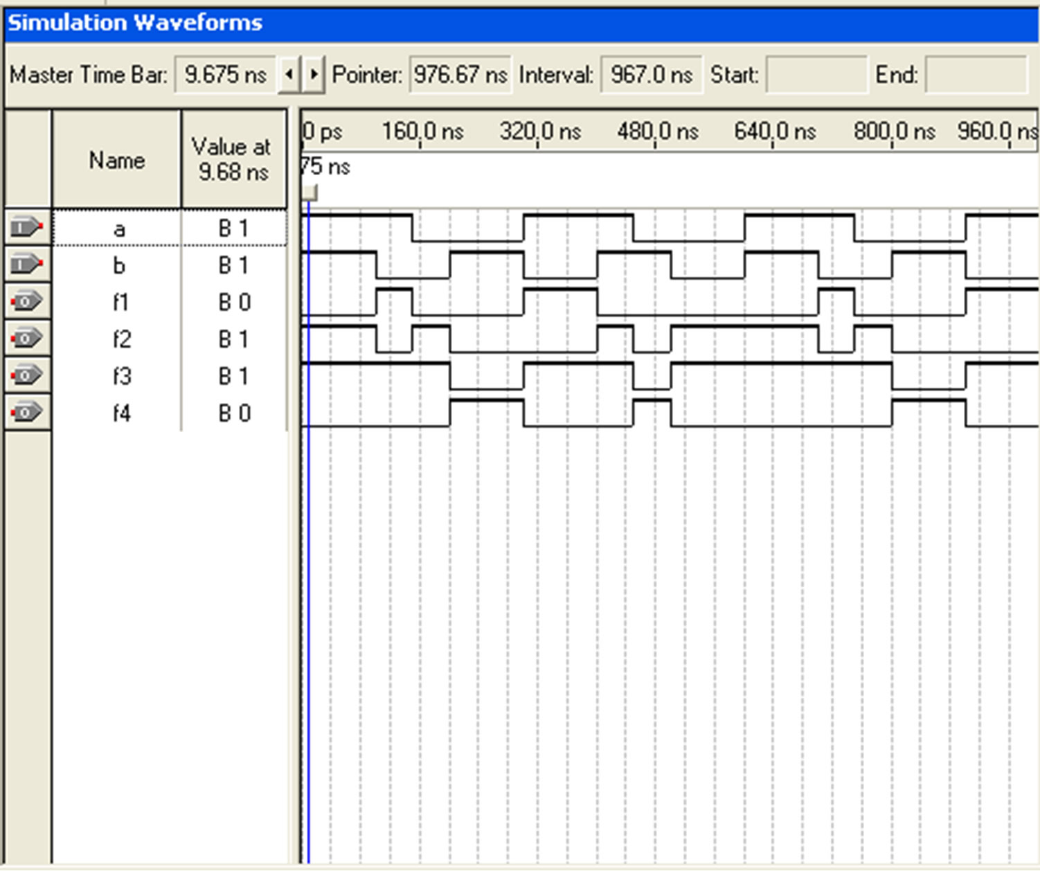 (c)
(c)
Figure 19. a) Three bit comparator a > b; b) Three bit comparator a = b; c) one bit comparator using DG gate.
menting concurrent EXOR and EXNOR output functions. Hence, three outputs of DG gate have efficient results for comparator designs. In this paper, one-bit comparator has better performance comparatively.
REFERENCES
- A. N. Nagamani, H. V. Jayashree and H. R. Bhagyalakshmi, “Novel Low Power Comparator Design Using Reversible Logic Gates,” 2011 Indian Journal of Computer Science and Engineering (IJCSE), Vol. 2, No. 4, 2011, pp. 566-574.
- R. Landauer, “Irreversibility and Heat Generation in the Computational Process,” IBM Journal of Research and Development, Vol. 5, No. 3, 1961, pp. 183-191. http://dx.doi.org/10.1147/rd.53.0183
- G. E. Moore, “Cramming More Components onto Integrated Circuits,” Electronics, Vol. 38, No. 8, 1965.
- C. H. Bennett, “Logical Reversibility of Computation,” IBM Journal of Research and Development, Vol. 17, 1973, pp. 525-532.
- M. Mohammadi and M. Eshghi, “On Figureures of Merit in Reversible and Quantum Logic Designs,” Quantum Information Processing, Vol. 8, No. 4, 2009, pp. 297-318. http://dx.doi.org/10.1007/s11128-009-0106-0
- D. Maslov and G. W. Dueck, “Improved Quantum Cost for n-Bit Toffoli Gates,” IEEE Electronics Letters, Vol. 39, No. 25, 2003, pp. 1790-1791. http://dx.doi.org/10.1049/el:20031202
- V. Vedral, A. Bareno and A. Ekert, “Quantum Networks for Elementary Arithmetic Operations,” 1995. arXiv:quantph/9511018 v1
- R. Feynman, “Quantum Mechanical Computers,” Optic News, Vol. 11, 1985, pp. 11-20. http://dx.doi.org/10.1364/ON.11.2.000011
- T. Toffoli, “Reversible Computing,” Tech memo MIT/ LCS/TM-151, MIT Lab for Comp. Sci, 1980.
- E. Fredkin and T. Toffoli, “Conservative Logic,” International Journal of Theoretical Physics, Vol. 21, No. 3-4, 1982, pp. 219-253. http://dx.doi.org/10.1007/BF01857727
- H. G. Rangaraju, V. Hegde, K. B. Raja and K. N. Muralidhara, “Design of Efficient Reversible Binary Comparator,” International Conference on Communication Technology and System Design, 7-9 December 2011.
- M. H. Azad Khan Md., “Design of Full Adder with Reversible Gate,” International Conference on Computer and Information Technology, Dhaka, 27-28 December 2002, pp. 515-519.
- H. R. Bhagyalakshmi and M. K. Venkatesha, “Design of a Multifunction BVMF Reversible Logic Gate and Its Applications,” International Journal of Computer Applications (0975-8887), Vol. 32, No. 3, 2011.
- H. Thapliyal and N. Ranganathan, “A New Design of the Reversible Subtractor Circuit,” 2011 11th IEEE International Conference on Nanotechnology, Portland Marriott, 15-18 August 2011.
- B. Dehghan, “Survey the Inverse Property of Quantum Gates for Concurrent Error Detection,” Journal of Basic and Applied Scientific Research, 2013, pp. 603-608.
NOTES
*Corresponding author.