Wireless Engineering and Technology
Vol.2 No.2(2011), Article ID:4541,8 pages DOI:10.4236/wet.2011.22007
MoM Analysis and Design of a Compact Coaxial-to-Microstrip Directional Coupler
![]()
1Preparatory School of Sciences and Technology (EPST-Tlemcen), Tlemcen, Algeria; 2University Abou Bekr Belkaid-Tlemcen, Tlemcen, Algeria.
Email: N_Benabdallah@yahoo.fr
Received November 24th, 2010; revised February 5th, 2011; accepted February 9th, 2011.
Keywords: Coaxial-to-microstrip coupler, Inhomogeneous asymmetrical coupler, A 20 dB compact directional coupler, Analysis and design, MoM method, CST MICROWAVE STUDIO software
ABSTRACT
In order to overcome the main drawbacks of coaxial, waveguide, and stripline couplers, the analysis and the design of a compact coaxial-to-microstrip directional coupler convenient for power and antenna control application, are presented using the method of moments (MoM) in two dimensions. This technique is adapted to study the complex configuration of the line’s system, which does not have a simple analytical solution. The modeling of this structure consists in analyzing the primary inductive and capacitive matrices ([L] and [C]). When these matrices are determined, it is possible to calculate the inductive and capacitive coupling coefficients (kL and kC) and estimate the resulting scattering parameters of the coupler using an adapted numerical model. The coupler can be integrated into a printed circuit board (PCB) and operates over 17 to 35 dB coupling coefficients and is always compensated. The compensation is achieved by the proper displacement of a tuning ground plane with respect to the edge of the PCB from 0.1 to 3.3 mm. As an application, we present the design of a compact coupler with 7.5 x 4.8 x 25.8 mm of size and having approximately 20 dB of coupling coefficient at 2 GHz and a minimum directivity of 23.3 dB in the frequency range [0.1 - 4] GHz. In order to check our numerical calculations by the MoM we made simulations in 3D by using CST MICROWAVE STUDIO software for the same geometrical and physical parameters of our designed coupler. The results obtained by the two numerical models (MoM and CST) show a good agreement of the frequency responses of the coaxial-to-microstrip directional coupler. The studied structure represents a great improvement for high power measurement systems, since it has broad-band, good directivity, and can be easily designed and fabricated.
1. Introduction
Integration of RF power, RF small, digital, DC and supervision circuits is still one of the main goals of modern radar, satellite and wireless communications technology. Today’s solutions of close-to-antenna devices use a stack approach for integration of RF filters with power splitters/combiners and multilayer printed circuit boards (PCB) containing the rest of the circuitry. One device that is difficult to integrate is a directional coupler mounted close to an antenna for the purpose of monitoring the transmitted and reflected powers. The requirements for such a coupler are of the high importance: very low insertion loss, very good matching and very good directivity (20 to 26 dB) [1].
A variety of different couplers are available from a number of manufacturers, including stripline couplers, waveguide couplers and coaxial configurations. Stripline or microstrip couplers are well suited for broad-band applications [2]; unfortunately their significant losses can prevent their use when high power handling is required. Waveguide Bethe-hole couplers are used in high power applications [3], but are not a practical solution for broad-band use. Although many techniques have been proposed for this purpose [4,5], the primary mode is limited at low frequencies by the cutoff frequency while the higher-order modes limit the upper-frequency extension. When bandwidth requirements are not critical, coaxial directional couplers using air dielectrics are a traditional solution [6], and would be ideal for their low-loss performance and high power-handling capabilities, with their transverse electromagnetic (TEM) field configurations ensuring zero cutoff frequency.
The author of the Reference [1] has introduced in the scientific literature a novel coupler structure convenient for power and antenna control application, where a 20 dB directional coaxial-to-microstrip coupler operating in the frequency range [1.5 - 2.5] GHz was analysed, designed and manufactured. Unfortunately, the designed coupler has a large size and presents a visible degradation directivity above 2.7 GHz.
The scope of this work is to analyse the same coupler configuration using the method of moment [7] in order to design a 20 dB directional compact coupler operating in the frequency range [1.5 - 2.5] GHz with a minimum directivity of 20 dB in the frequency range [0.1 - 4] GHz.
2. Coaxial-to-Microstrip Coupler
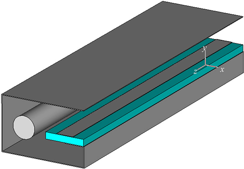
The 3D representation and the cross section of the coaxial-to-microstrip coupler are respectively shown in Figures 1(a) and 1(b). The coupler is composed of a coaxial line (main line, carrying the power) and a microstrip with dielectric constant (er), as the coupled line, placed beside the coaxial line.
In this structure, only the coupled line is embedded into the PCB. The dielectric material protrudes past the edge of the tuning ground plane (s), towards the center conductor of the coaxial line at a distance (s2).
For this type of coupler, the coupling level can be adjusted by the displacement of the tuning ground plane with respect to the edge of the PCB (s2) and also by changing the suspension level of the PCB (h2) or by changing the distance between the coupled lines (s0 + s1) [8].
3. Numerical Resolution
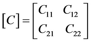
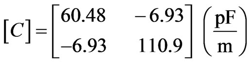
The electrical properties of the lossless and inhomogeneous asymmetrical coupler presented in Figure 1 can be described in terms of its primary parameters [L] and [C], and its secondary parameters kL and kC.
where: 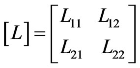 ;
; 
The inductance matrix [L] contains the self-inductances on the diagonal (L11 and L22 are the proper inductances respectively of the coaxial line and of the microstrip line) and the mutual inductances (L12 = L21) between the two lines.
Matrix [C] accounts for the capacitative effects between the two lines, characterizing the electric field energy storage in the coupler (C11, C22 are the proper capacitances respectively of the coaxial and of the microstrip lines and (C12 = C21) is the coupling capacitance of the coupler).
and 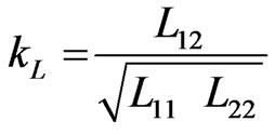 ;
; 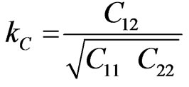
are respectively the inductive and capacitive coupling coefficients.
The numerical calculations of the primary inductive and capacitive matrices ([L] and [C]) of the coaxial-tomicrostrip coupler were carried out with LINPAR for windows (Matrix Parameters for Multiconductor Transmission Lines), a 2D method of moments (MoM) software for numerical evaluation of the quasi static matrices for multiconductor transmission lines embedded in piecewise-homogeneous dielectrics [7].
Using LINPAR, these matrices are evaluated from the electrostatic analysis of two systems. The first system coincides with the studied coupler, and the analysis results in the matrix [C]. The second system is obtained by removing the dielectrics of the coupler and replacing them with a vacuum (while the conductors remain intact). The analysis results in the matrix [L].
Both electrostatic problems are solved concurrently by using the same numerical technique. First, a set of integral equations is formulated for the total (free plus bound) charges of the system. Second, these equations are solved using the method of moments to yield the charge distribution. Third, the primary matrix parameters are found based on this distribution.
In the following, we present the numerical procedure that is used in LINPAR for windows [7].
 (a)
(a)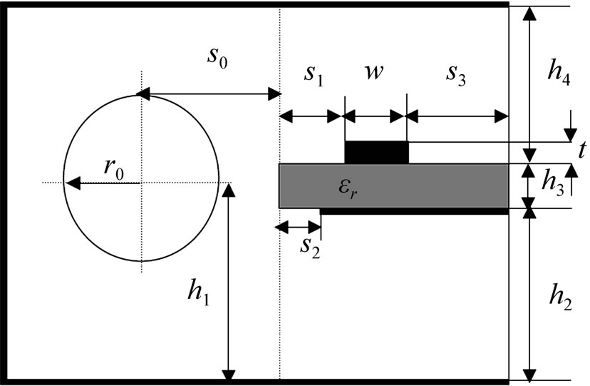 (b)
(b)
Figure 1. The coaxial-to-microstrip coupler: (a) The 3D representation; (b) The cross section.
3.1. Integral Equations for Charge Distribution
Suppose that the studied coupler has three different dielectrics. One of them is of permittivity e1, the other one is of permittivity e2, while the dielectric in the remaining space is a vacuum (of permittivity e0). The conductors of the coupler are at a certain potential with respect to the reference conductor (the shield), and the free charges are located at the conductor surfaces. The objective is to find the distribution of these charges.
The influence of the dielectrics on the electric field and potential can be completely described by the influence of dielectric bound charges located in a vacuum. Thus, the electric field and the potential are the same in the original coupler and in the equivalent coupler where the dielectrics are replaced by bound charges in a vacuum.
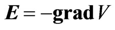
First, a set of integral equations are formulated for the charge distribution. One part of this set is derived based on the boundary conditions for the conductors. The electrostatic potential V of each conductor can be expressed in terms of the surface densities of the free and bound charges as
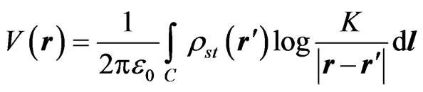 , (1)
, (1)
where r is the position-vector of the field point (the point at which the potential is evaluated), r' is the position-vector of the source point (the point at which the charges are located), rst = rs + rsb is the total-charge surface density, rs is the free-charge density, rsb is the bound-charge density, dl is the element of the conductor or dielectric boundary contour (C), V is the conductor potential, and K is an arbitrary constant.
For each signal conductor and for the reference conductor one equation of the form (1) is formulated, setting the potential to be equal to the actual conductor potential. Each of these equations is an integral equation for the total-charge density.
The integral of the free-charge density for all conductors must be zero to provide a finite per-unit-length energy of the coupler, and the integral of the bound-charge density is also zero, due to the nature of these charges. Hence,
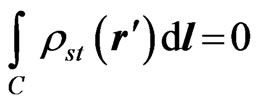 , (2)
, (2)
which is another integral equation to be satisfied by the charges.
The remaining part of the set of integral equations is formulated based on the boundary conditions for the normal component of the electric field at the dielectricto-dielectric interfaces.
Consider an interface between two dielectrics, of permittivities e1 and e2, respectively. The boundary conditions require that
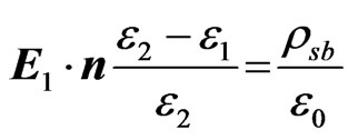 , (3)
, (3)
where E1 is the electric field in the first dielectric just at the boundary, and  is the unit normal on the boundary surface, directed from the second toward the first dielectric. The electric field in equation (3) can be expressed as
 , (4)
, (4)
and the potential V can be substituted from equation (1), so that equation (3) also represents an integral equation in rst, yielding
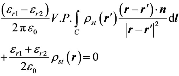 (5)
(5)
where er1 and er2 are the relative permittivities of the dielectrics at the two sides of the field segment, and V.P. denotes that the principal value of the integral is evaluated to avoid dealing with the electric-field singularity for r = r'. However, the electric field produced by the local charges has been included through the term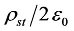 . Equations of form (5) are formulated for each dielectric-to-dielectric interface.
3.2. Solution of Integral Equations for Charge Distribution
Generally, the set of integral equations (1), (2), and (5) can only be solved numerically. The general idea of the method of moments is as follows [9].
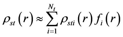
First, the unknown total-charge distribution is approximated by dividing each boundary (i.e. conductor surface and dielectric-to-dielectric interface) into a number of infinitely long segments. The total number of segments is
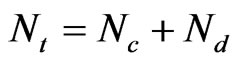 , (6)
, (6)
where Nc is the number of segments for all conductor surfaces, and Nd the number of segments for all dielectric-to-dielectric interfaces. In the cross section of the coupler, each segment appears as a straight line.
Each segment assumed to carry a uniformly distributed total charge, which corresponds to the so-called pulse approximation (piecewise-constant approximation) for the charge distribution. In term of the method of moments, this procedure can be represented as adopting expansion (basis) functions
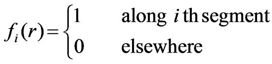 , (7)
, (7)
so that
 , (8)
, (8)
where rsti are unknown constants to be solved, and r is the position vector.
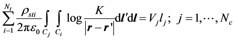
Instead of the point-matching technique used in [10] and [11], here the Galerkin technique is used [9,12], which generally results in a smaller overall number of unknowns for a given accuracy and, thus, in a more efficient computer program. This technique corresponds to using functions (7) for testing as well as expansion.
The approximation (8) is next substituted into equations (1) and (5), and the inner products of these equations and the testing functions are evaluated. Each inner product is obtained by multiplying the corresponding equation with a testing function and then integrating along the segment where the testing function is defined.
Equations (1) and (5) finally yield the following system of linear equations in rsti:
 (9)
(9)
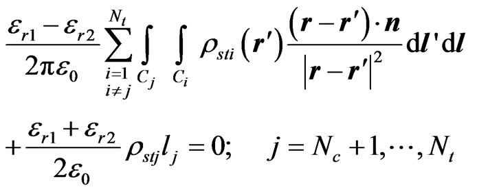 (10)
(10)
where dl' is an element of the source segment (Ci), dl is an element of the field segment (Cj), and lj is the length of the jth segment.
The resulting system of linear equations is solved using the LU-decomposition. Once the total surface charges are evaluated, it is necessary to find the free-charge density on the conductor surfaces, as the free charges will further be required to evaluate the primary matrix parameters.
The conductors of the second electrostatic system, used in the evaluation of the matrix [L], coincide with the conductors of the first system, used in the evaluation of the matrix [C]. The two systems of linear equations can be solved simultaneously, taking care with the pivotization, so that the solution of the second electrostatic system adds very little computational time to the solution of the first one.
In order to analyse our coaxial-to-microstrip directional coupler under LINPAR environment, we were obliged to supply the cross sections of the structure and all relevant dielectrics characteristics including the segmentation by using our programs done in FORTRAN.
When the matrices [L] and [C] are determined, it is possible to calculate the inductive and capacitive coupling coefficients values (kL and kC) and estimate the resulting scattering parameters of the coupler using an adapted numerical model [13].
For this type of inhomogeneous and asymmetrical coupler, it is known that the 50 W matched coupler can be compensated if the coupled lines are terminated with their proper impedances (i.e. 50 W) and if the inductive and capacitive coupling coefficients are equalized.
4. MoM Results
First, we analyzed the coaxial line with rectangular shielding (Figure 2), in order to find the parameters values of the 50 W matched line for s0 = 2 mm, h1 = 2.4 mm and er = 1. The curve of Figure 3 reveals the influence of the inner conductor radius (r0) on the characteristic impedance of the line.
Then, in order to find the 50 W matched coupled microstrip line, the displacement of the tuning ground plane (s2) was varied from 0.1 to 3.3 mm as needed to change the characteristic impedance of the line (Figure 4). The line was analyzed with the following features: h1 = 2.4 mm, h2 = 1.8 mm, h3 = 0.6 mm, h4 = 2h1 – (h2 + h3), s1 = 1 mm, s3 = 1 mm, w = 1.5 mm, t = 0.035 mm and er = 4.8.
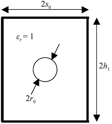
Figure 2. The cross section of the rectangular coaxial line.
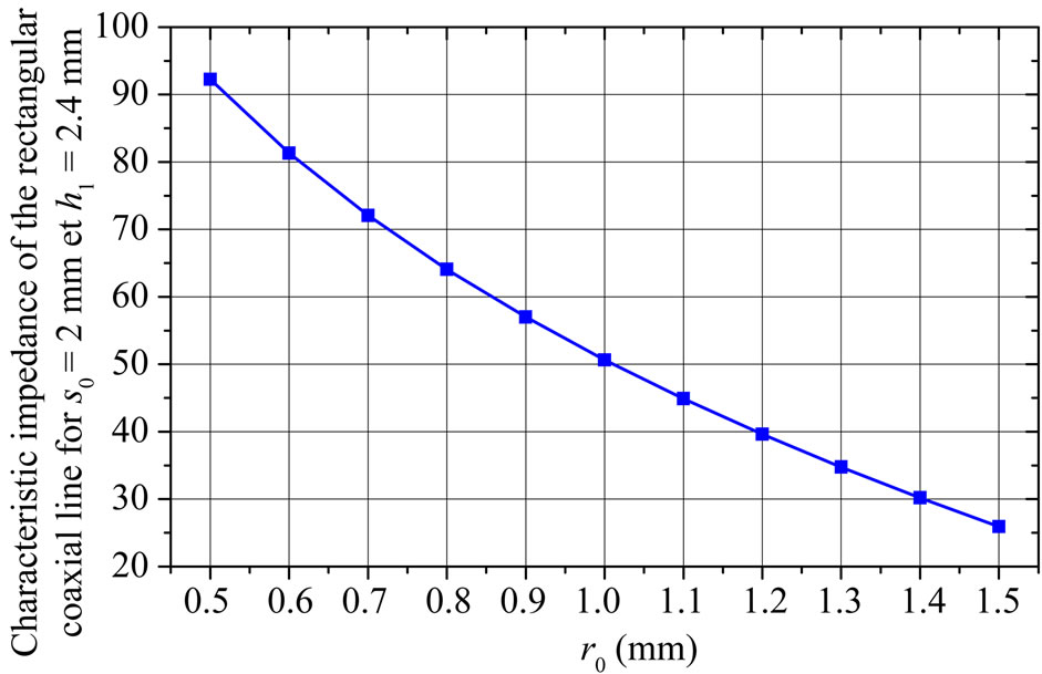
Figure 3. Influence of the inner conductor radius (r0) on the characteristic impedance of the coupled coaxial line.
Figure 5 shows the influence of the tuning ground (s2) on the characteristic impedance of the coupled microstrip line The characteristic impedance of 50 W for the rectangular coaxial and the coupled microstrip lines is obtained respectively for r0 = 1 mm and s2 = 1.8 mm.
Finally, we applied the MoM-based numerical tool to the analysis and design of the asymmetrical coaxialto-microstrip coupler. The MoM approach makes it possible to simulate the performance of a design and decides if a given set of constraints makes it possible to realize the coupler.
The segmentation of the charged surfaces of the compact coaxial-to-microstrip coupler using LINPAR is shown in Figure 6 with the following features: r0 = 1 mm, h1 = 2.4 mm, h2 = 1.8 mm, h3 = 0.6 mm, h4 = 2h1 – (h2 + h3), s1 = 1 mm, s2 = 1.8 mm, s3 = 1 mm, w = 1.5 mm, t = 0.035 mm and er = 4.8.
In this work, the coupling level was adjusted by the displacement of the tuning ground plane with respect to the edge of the PCB (s2). Figures 7 and 8 show the influence of the tuning ground (s2) on the electromagnetic parameters ([L] and [C]) of the coaxial-to-microstrip coupler. These curves are necessary for the design of the coaxial-to-microstrip coupler using MATPAR [13].
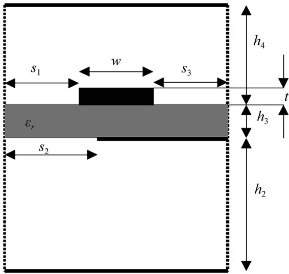
Figure 4. The cross section of the coupled microstrip line.
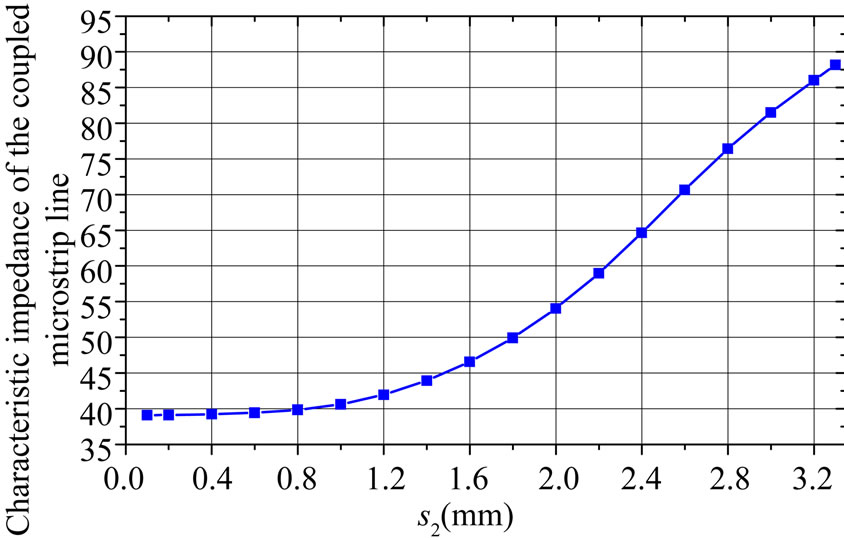
Figure 5. Influence of the tuning ground (s2) on the characteristic impedance of the coupled microstrip line.
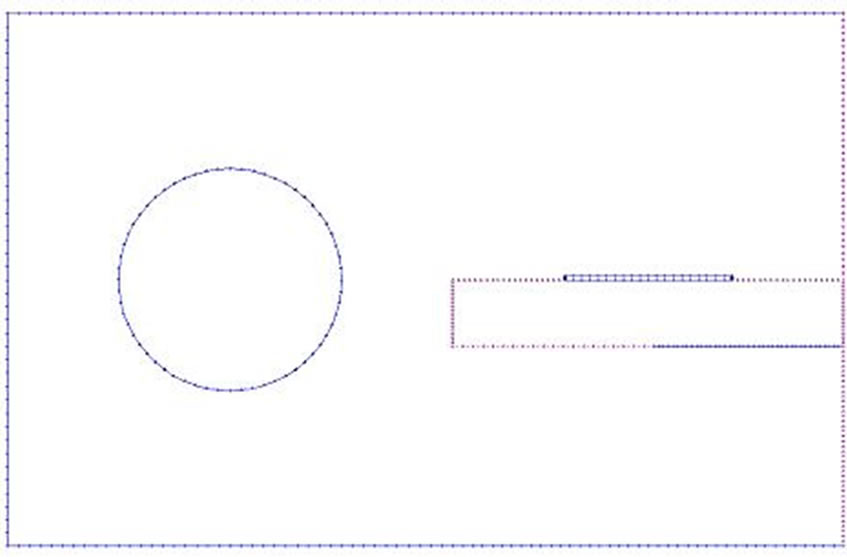
Figure 6. The segmentation of the charged surfaces used to analyse the cross section of the compact coaxial-to-microstrip coupler.

Figure 7. Influence of the tuning ground (s2) on the elements of the inductance matrix [L] of the coupler.
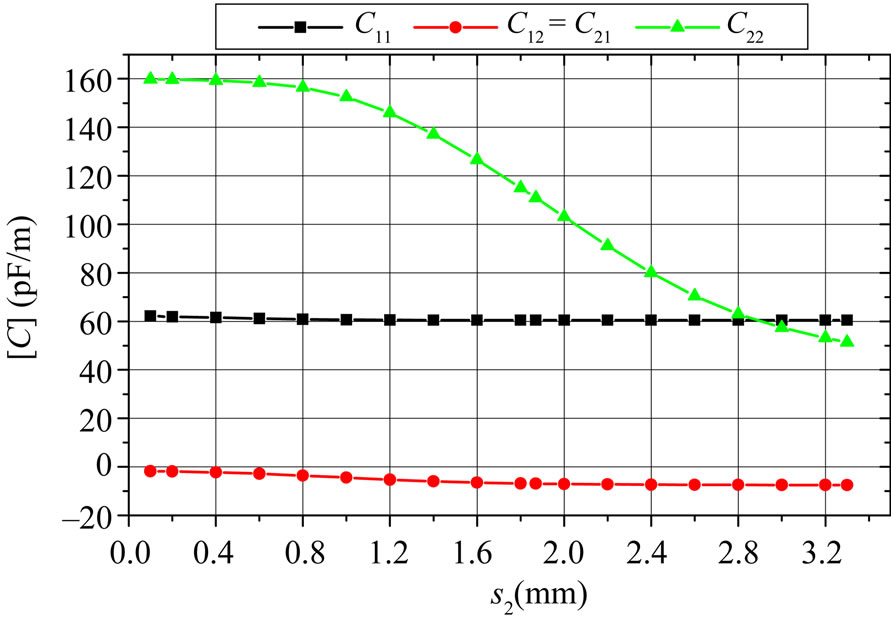
Figure 8. Influence of the tuning ground (s2) on the elements of the capacitance matrix [C] of the coupler.
The effects of the tuning ground (s2) on the inductive and capacitive coupling coefficients of the coaxial-tomicrostrip coupler are shown in Figure 9. It appears clearly from this figure that the inductive coupling coefficient kL and the capacitive coupling coefficient kC are equal for s2 = 1.87 mm.
5. Directional Coupler
In the following, we interest to the design of a 20 dB directional compact coupler operating in the frequency range [1.5 - 2.5] GHz with a minimum directivity of 20 dB in the frequency range [0.1 - 4] GHz.
The Figure 10 presents the structure of a four port coupler, where all the ports are matched with 50 W.
In order to make an effective design possible it is necessary to equalize the inductive and the capacitive coupling coefficients.
Consequently, for a tuning ground s2 = 1.87 mm, the primary and secondary parameters of the coupler are:
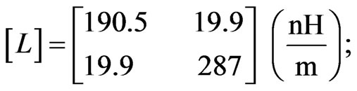
kL = –21.40 dB and kC = –21.45 dB.
In the Reference [1], the length of the coupler obtained for air solutions 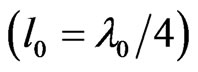 is reduced approximately by a
 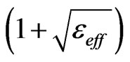 factor, where eeff is the effective dielectric constant for the mode associated with the coupled line embedded in the dielectric material of the PCB.
In this work, we found that the length of the inhomogeneous asymmetrical coupler can be expressed by the following relation:
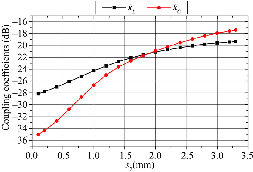
Figure 9. Effects of the tuning ground (s2) on the coupling coefficients of the coaxial-to-microstrip coupler.
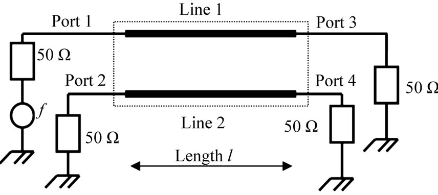
Figure 10. Coupler.
 (11)
(11)
In order to show the usefulness of this relation, Figure 11 provides plots of the resulting scattering parameters of the coupler (with respect to 50 W) and operating at different frequencies (1 to 5 GHz).
For a length l = 25.8 mm, the response of the compact coupler with 7.5 x 4.8 x 25.8 mm of size, obtained by the MoM results, is shown in Figure 12. The designed coupler operating in the frequency range [1.5 - 2.5] GHz has approximately a 20 dB of coupling coefficient at 2 GHz and a minimum directivity of 23.3 dB in the frequency range [0.1 - 4] GHz.
In order to check our numerical calculations by the MoM we made simulations in 3D by using the Transient Solver of CST MICROWAVE STUDIO software for the same geometrical and physical parameters of our designed coupler [14].
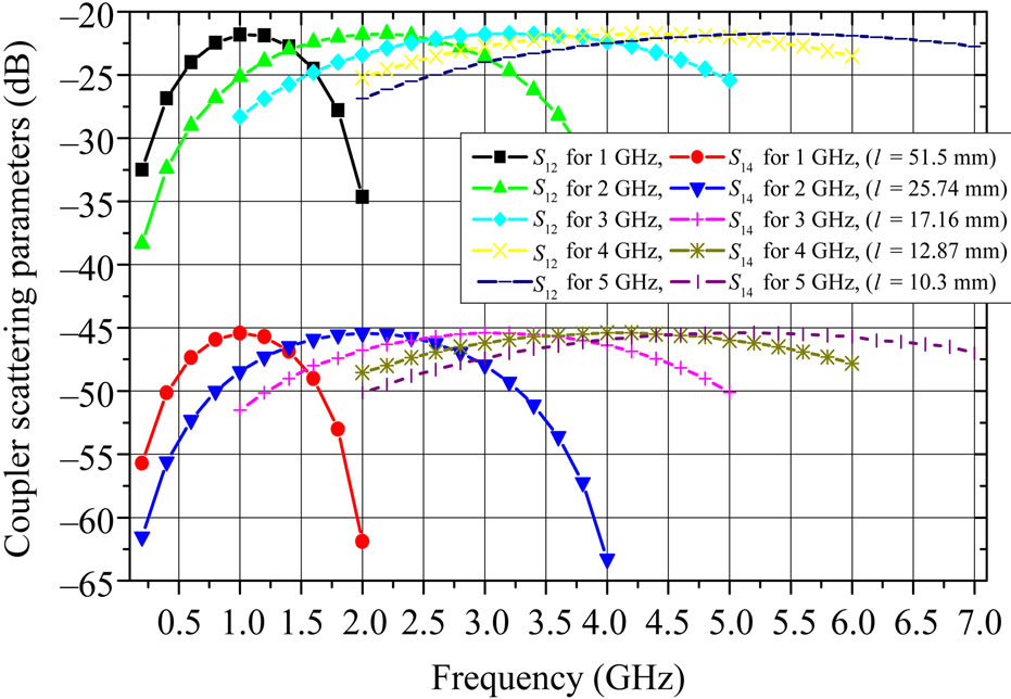
Figure 11. Choice length of the inhomogeneous asymmetrical coupler.
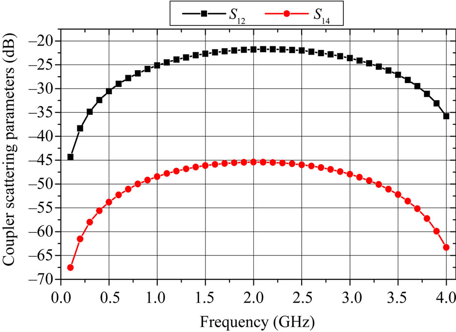
Figure 12. Response of the compact coupler operating at 2 GHz.
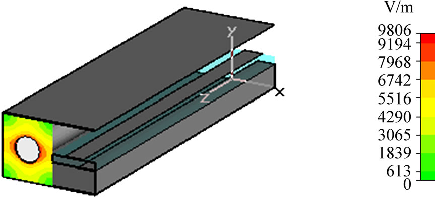
The CST approach was employed to analyze the compact coaxial-to-microstrip directional coupler having the geometrical parameters obtained by the MoM as shown in Figure 13.
It is found that the characteristic impedances of the main line, carrying the power (coaxial line) and the coupled line (microstrip line) are respectively 50.58 W (Figure 13(a)) and 49.28 W (Figure 13(b)). These values show a good agreement with those fixed in the MoM-design of the coupler.
Finally, we show in Figure 14 the scattering parameters of the compact coaxial-to-microstrip directional coupler obtained using CST.
From Figures 12 and 14, it appears clearly that the frequency responses of the coaxial-to-microstrip directional coupler obtained by the two numerical models (MoM and CST) are in a good coherence.
 (a)
(a)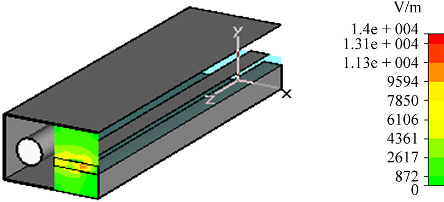 (b)
(b)
Figure 13. Simulations using CST.
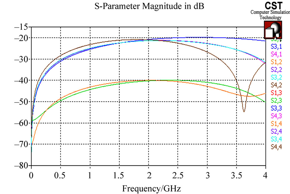
Figure 14. Response of the compact coupler using CST.
6. Conclusions
A 20 dB directional coupler with a wide bandwidth using coaxial-to-microstrip coupling structure has been analyzed and designed. The designed compact coupler with 7.5 x 4.8 x 25.8 mm of size, has approximately 20 dB of coupling coefficient at 2 GHz and a minimum directivity of 23.3 dB in the frequency range [0.1 - 4] GHz.
The structure represents a great improvement for high power measurement systems and can be easily designed and fabricated.
To reach this objective, it was necessary to determine the electromagnetic parameters of the structure ([L], [C], kL and kC). In the frequency range [0.1 - 4] GHz, the resolution of the problem is based on the quasi-static assumption and was made by the method of moment.
The quasi-static design, presented in this article, makes an effective design possible based on the equalization of inductive and capacitive coupling coefficients. Also the length of the coupler obtained for air solutions is reduced approximately by a 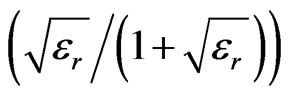 factor, where er is the dielectric constant of the coupled microstrip line.
In order to check our numerical calculations by the MoM we made simulations in 3D by using CST MICROWAVE STUDIO software for the same geometrical and physical parameters of the MoM-designed coupler.
The results obtained by the two numerical models (MoM and CST) show a good agreement of the frequency responses of the coaxial-to-microstrip directional coupler.
All the curves presented in this article, taking into account the influence of the tuning ground on the electromagnetic parameters of the studied coupler, prove the interest of the CAO program developed.
REFERENCES
- A. Sawicki, “A New Class of Asymmetrical Directional Couplers for Power/Antenna Control Applications,” Microwave Journal, Vol. 48, No. 11, November 2005, pp. 102-112.
- S. Uysal and H. Aghvami, “Synthesis, Design, and Construction of Ultra-Wide-Band Nonuniform Quadrature Directional Couplers in Inhomogeneous Media,” IEEE Transactions on Microwave Theory and Techniques, Vol. 37, No. 6, June 1989, pp. 969-976. doi:10.1109/22.25398
- R. E. Collin, “Foundations for Microwave Engineering,” 2nd Edition, McGraw-Hill, New York, 1992.
- H. Schmiedel and F. Arndt, “Field Theory Design of Rectangular Waveguide Multiple-Slot Narrow-Wall Couplers,” IEEE Transactions on Microwave Theory and Techniques, Vol. MTT-34, July 1986, pp. 791-798. doi:10.1109/TMTT.1986.1133442
- L. T. Hildebrand, “Results for a Simple Compact NarrowWall Directional Coupler,” IEEE Microwave and Guided Wave Letters, Vol. 10, No. 6, June 2000, pp. 231-232. doi:10.1109/75.852425
- A. H. McCurdy and J. J. Choi, “Design and Analysis of a Coaxial Coupler for a 35-GHz Gyroklystron Amplifier,” IEEE Transactions on Microwave Theory and Techniques, Vol. 47, No. 2, February 1999, pp. 164-175. doi:10.1109/22.744291
- A. R. Djordjevic, M. B. Bazdar and T. K. Sarkan, “LINPAR for Windows: Matrix Parameters of Multiconductor Transmission Lines, Software and User’s Manual,” Artech House, London, 1999.
- N. Benahmed and N. Benmostefa, “Design Directional Couplers for High Power Applications,” Microwaves & RF, Vol. 45, No. 10, October 2006, pp. 90-98.
- R. F. Harrington, “Field Computation by Moment Methods,” Macmillan, New York, 1968.
- W. Cao, R. F. Harrington, J. R. Mautz and T. K. Sarkar, “Multiconductor Transmission Lines in Multilayered Dielectric Media,” IEEE Transactions on Microwave Theory and Techniques, Vol. 32, No. 4, April 1984, pp. 439- 450. doi:10.1109/TMTT.1984.1132696
- J. Venkataraman, S. M. Rao, A. R. Djordjevic, T. K. Sarkan and N. H. Yang, “Analysis of Arbitrary Oriented Microstrip Transmission Lines in Arbitrary Shaped Dielectric Media over a Finite Ground Plane,” IEEE Transactions on Microwave Theory and Techniques, Vol. 33, No. 10, October 1985, pp. 952-960. doi:10.1109/TMTT.1985.1133155
- M. B. Bazdar, “Evaluation of Matrix Parameters of Multiconductor Transmission Lines by the Galarkin Method,” M.Sc. Thesis, School of Electrical Engineering, University of Belgrade, Belgrade, 1991.
- A. R. Djordjevic, M. Bazdar, G. Vitosevic, T. Sarkar and R. F. Harrington, “Scattering Parameters of Microwave Networks with Multiconductor Transmission Lines,” Artech House, London, 1990.
- CST-Computer Simulation Technology, 2010. http://www.cst.com