Energy and Power Engineering
Vol.5 No.6(2013), Article ID:35708,10 pages DOI:10.4236/epe.2013.56042
Comparison and Evaluation of Power Factor Correction Topologies for Industrial Applications
1Laboratory of Electromechanical Energy Conversion (LEMEC), Department of Electrical and Computer Engineering, University of Patras, Patras, Greece
2Department of Electrical Engineering, TEI of Lamia, Lamia, Greece
3MILTECH HELLAS S.A., Koropi, Greece
Email: jkaratzaferis@ece.upatras.gr, npapanikolaou@teilam.gr, e.c.tatakis@ece.upatras.gr, mloupis@teilam.gr, jspa@miltech.gr
Copyright © 2013 John Karatzaferis et al. This is an open access article distributed under the Creative Commons Attribution License, which permits unrestricted use, distribution, and reproduction in any medium, provided the original work is properly cited.
Received June 14, 2013; revised July 14, 2013; accepted July 21, 2013
Keywords: Power Factor Correction; Industrial Load; Converter; Thermal Design; Mass/Volume Analysis
ABSTRACT
Power factor correction is a major issue for all industries, since a typical industrial load is causing current delays, as well as higher order current harmonics. Power factor correction is often mandatory from the power companies, usually by charging the reactive power that the company consumes. Many solutions for power factor correction have been presented in the bibliography; in this paper, the most significant power factor correction topologies will be reviewed and simulated with SABER RD software. Finally, a prototype design will be presented, based on a mass/cost analysis of the selected topologies and with an aim to manufacture 10 kW modules. The main outcome of this work is the feasibility for an SME to manufacture a competitive modular power factor correction product for industrial applications.
1. Introduction
A typical industrial unit contains a large number of nonunity power factor loads. Motor drives and ballast lighting are among the most significant industrial loads that cause current displacement angle, as well as higher order harmonic currents. Thus, power factor correction topologies are mandatory in order to reduce the impact of these loads to the grid. Most of the large industrial units have already installed reactive power compensators in order to reduce the reactive power consumed by the unit, and increase the power factor of the whole unit. However, the level of integration of such technologies in small and medium enterprises (SMEs) is not satisfactory. This is mainly due to the fact that purchasing such equipment is not expected to have a justifiable economic payback for enterprises of this size. Thus, a low budget solution needs to be implemented. In this paper, an analysis and evaluation of different threephase power factor correction topologies for industrial use is carried out. The criteria used for the evaluation are mainly cost related; the topologies are examined with regard to their cost (EUR/kW), efficiency, and power density (kg/kW).
2. Topologies under Evaluation
The main industrial load is the induction machine, usually controlled by a motor drive, fed by a DC bus. The DC bus is formed by rectifying the grid voltage, normally using a diode bridge. For some special applications, a DC machine is used, which is usually controlled by a 6 pulse thyristor controlled rectifier. In either case, the load causes a delay of the input fundamental harmonic current, as well as higher order harmonics due to its non-linearity. The power factor of a load is given by:
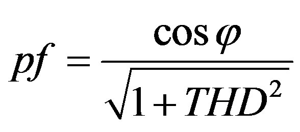 (1)
(1)
where φ is the displacement angle of the current fundamental harmonic and
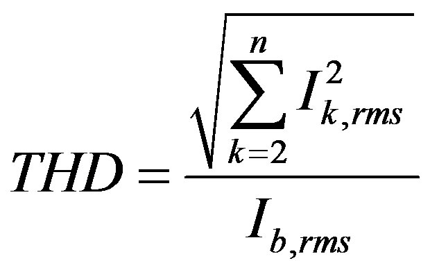 (2)
(2)
where 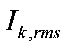 is the rms value of the k-th order current harmonic and
 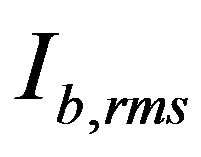 is the rms value of the fundamental current harmonic.
Ideally, the power factor should be equal to 1, thus, the angle φ as well as the THD factor should be set to zero. This can be achieved by adding a power factor correction topology, either using a cascade connection scheme (Figure 1), or a parallel connection scheme (Figure 2). In the cascade connection scheme, a power factor correction rectifier is used is series with the motor drive, substituteing its input stage, which is normally a diode bridge. This leads to unity power factor at the input. On the other hand, using a parallel configuration, a power factor correction topology, (usually an active filter) is placed in parallel with the rectifier input, in order to supply a current, such that the total input current has zero distortion, and zero phase delay.
Here, the most significant topologies for use in a cascade or parallel connection scheme will be briefly presented and an evaluation will be performed, based on simulation results.
2.1. Topologies for Cascade Connection Scheme
2.1.1. Boost Topologies for PFC Operation
The main feature of this PFC family is the boost operation, meaning that the output voltage is higher than the peak line-to-line grid voltage. Depending on the control method and the complexity of the design there is a wide variety of converters.
1) Vector or Direct Power Controlled Boost PFC Rectifiers [1,2]
This type of PFC rectifiers (Figure 3) includes a vector or direct power controlled inverter, operating as a rectifier. By controlling the power flow at the d-q axes, unity power factor can be achieved. This family of converters offers high quality PFC operation and good power density and is a good solution for high power applications.
2) PFC Rectifiers with Parallel or Series Connected Dual Boost Topology [3-5]
This family of PFC converters (Figure 4) includes the rectifiers with parallel or series connected dual-boost topology. The basic configuration includes a bridge rectifier and three switches, delta or star connected, depending on the operation mode. For any given time interval, one of the three switches remains constantly on and the other two are controlled usually by the one shot control method. This results in two controlled boost rectifiers forming the line currents. Depending on the configura-
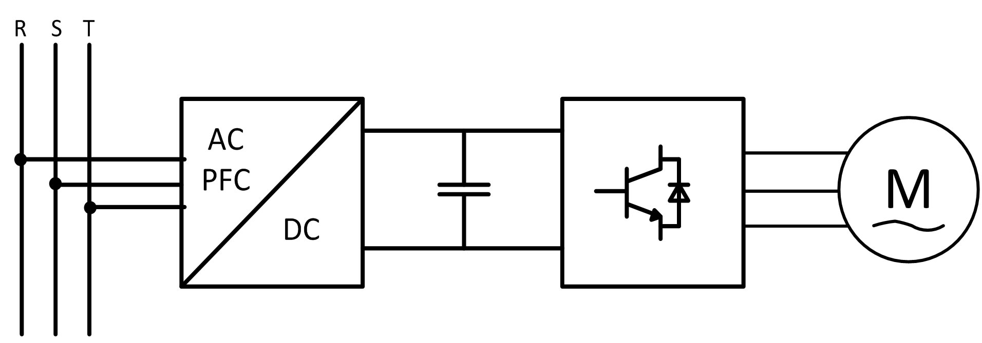
Figure 1. Cascade connection scheme.
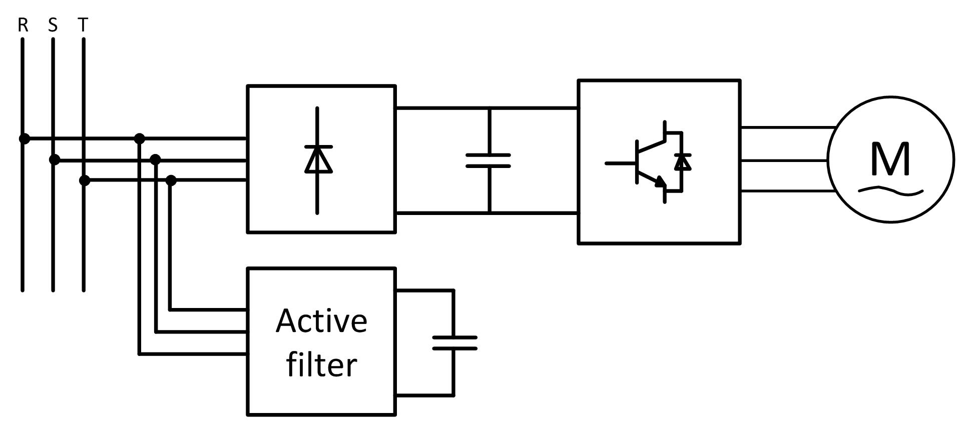
Figure 2. Parallel connection scheme.
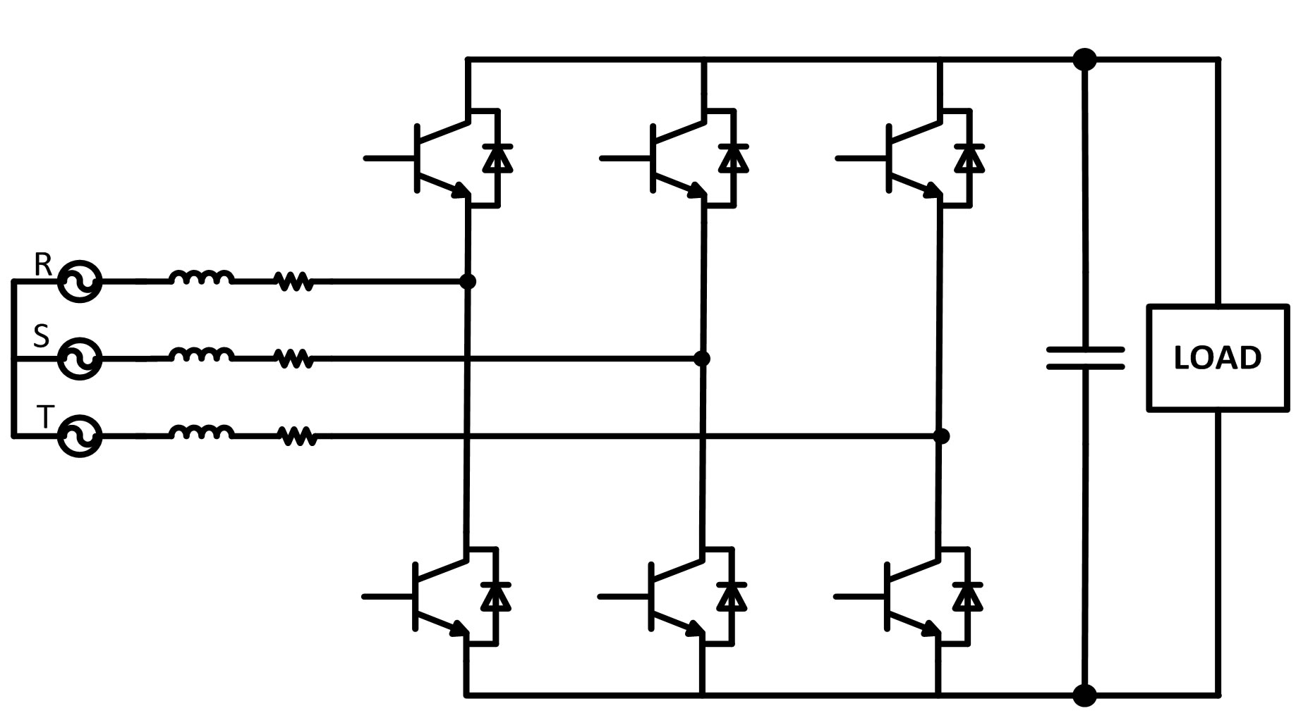
Figure 3. Vector or direct power controlled PFC rectifiers.
tion of the switches, the boost converters may be parallel connected, or series connected (Vienna rectifier).
3) Half Controlled Boost Rectifiers [6]
This family of PFC rectifiers (Figure 5) contains fewer semiconductor switches, offering higher power density and simpler control. However, the control is not effective throughout the whole line period, thus higher order current harmonics appear.
4) Single Switch Boost PFC Rectifiers [7,8]
This topology includes only one PWM operated semiconductor switch (Figure 6), hence it results to high power density and simple control. The duty cycle of the switch is always such that the input inductors’ currents are fully discharged during every switching cycle. When the switch is on, a virtual, neutral point is created and as a result, the inductors’ currents are increased at a rate proportional to the instantaneous values of the respective line voltages. Consequently, at the end of each switching cycle the inductors peak currents can be considered proportional to the instantaneous line voltages, under the
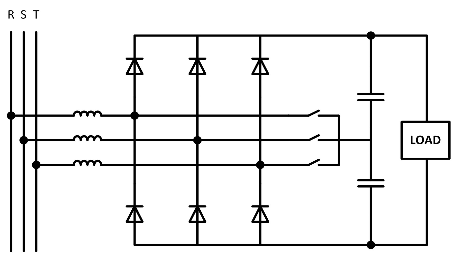
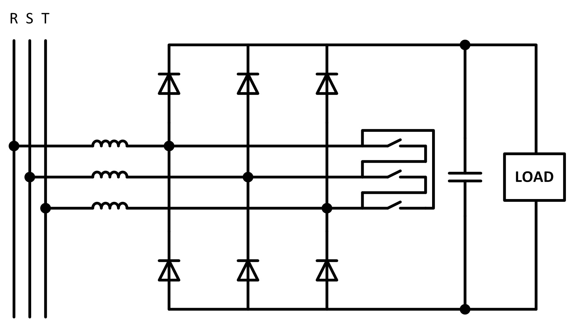
Figure 4. PFC rectifiers with series (upper case) or parallel (lower case) dual boost topology.
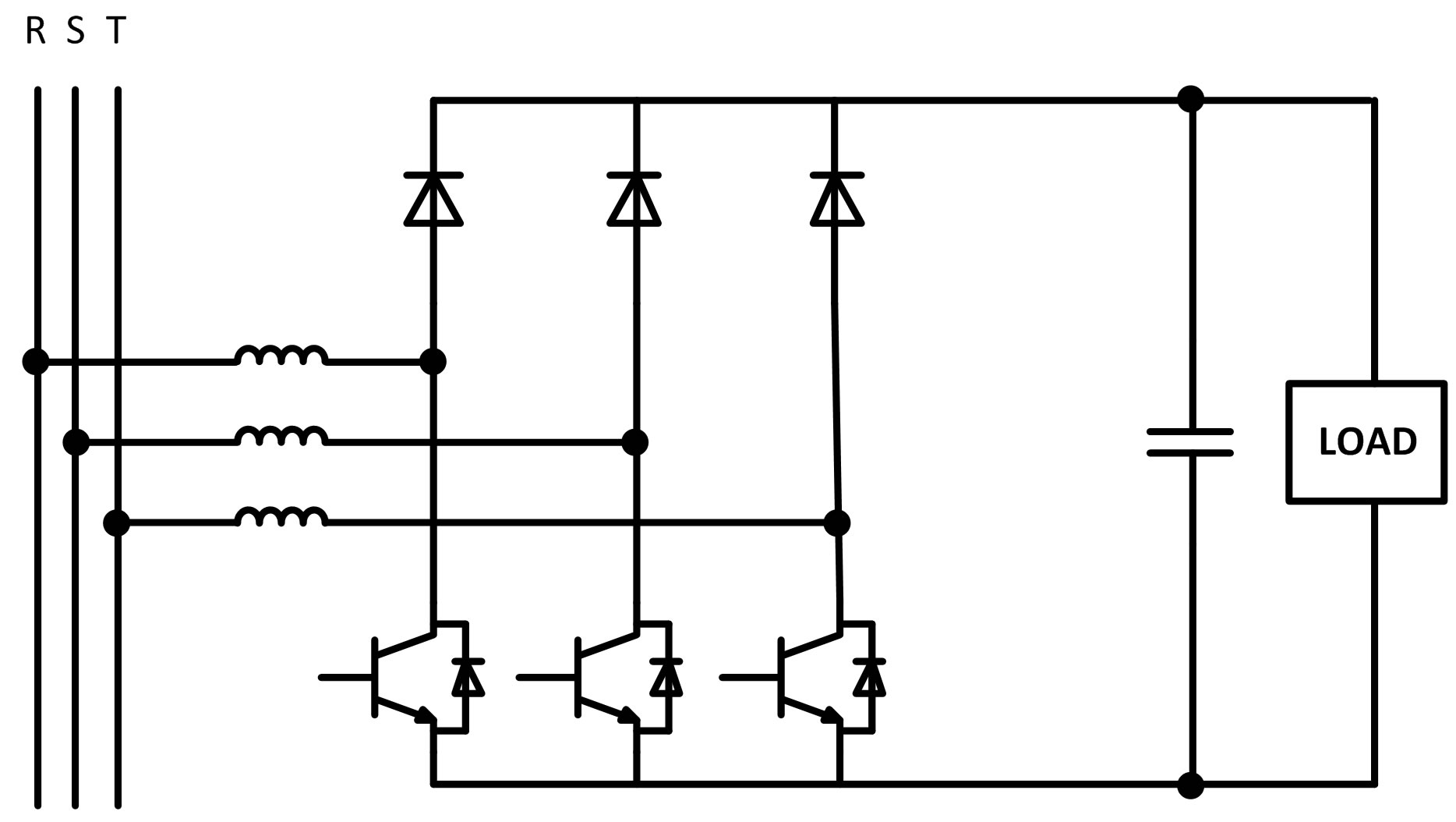
Figure 5. Half controlled boost PFC rectifier.
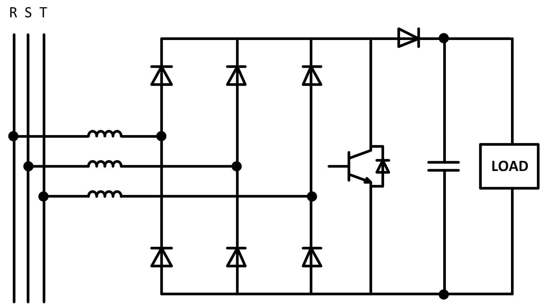
Figure 6. Single switch boost PFC rectifier.
assumption that the switching frequency is significantly higher than the line frequency and—after applying filtering—almost unity power factor can be achieved. It is also worth mentioning that no input voltage sensing is required for operation.
2.1.2. Buck PFC Topologies for Cascade Connection Schemes
When lower voltage is required for specific applications, (electrolysis, battery charging etc.), a buck PFC topology may be used.
1) Fully Controlled Buck Rectifier [9,10]
For this topology (Figure 7), the switches are placed at the input, to meet the case of a buck converter. During any given time interval, one switch should remain constantly on, and the rest should be PWM controlled, to achieve unity power factor. Usually the control method is the charge control.
2) Single Switch Buck Rectifier [11]
This topology contains only one semiconductor switch, offering higher efficiency and power density for buck PFC operation (Figure 8). However, due to the simple design, higher harmonic current elimination is not as effective as with other topologies.
3) Buck-Boost Topologies [12,13]
This family of converters offers buck-boost capability, meaning that the output voltage has no upper or lower limit (Figure 9). However, some topologies may suffer low efficiency, due to the large number of semiconductor switches required for buck-boost operation, and may be unsuitable for high power applications.
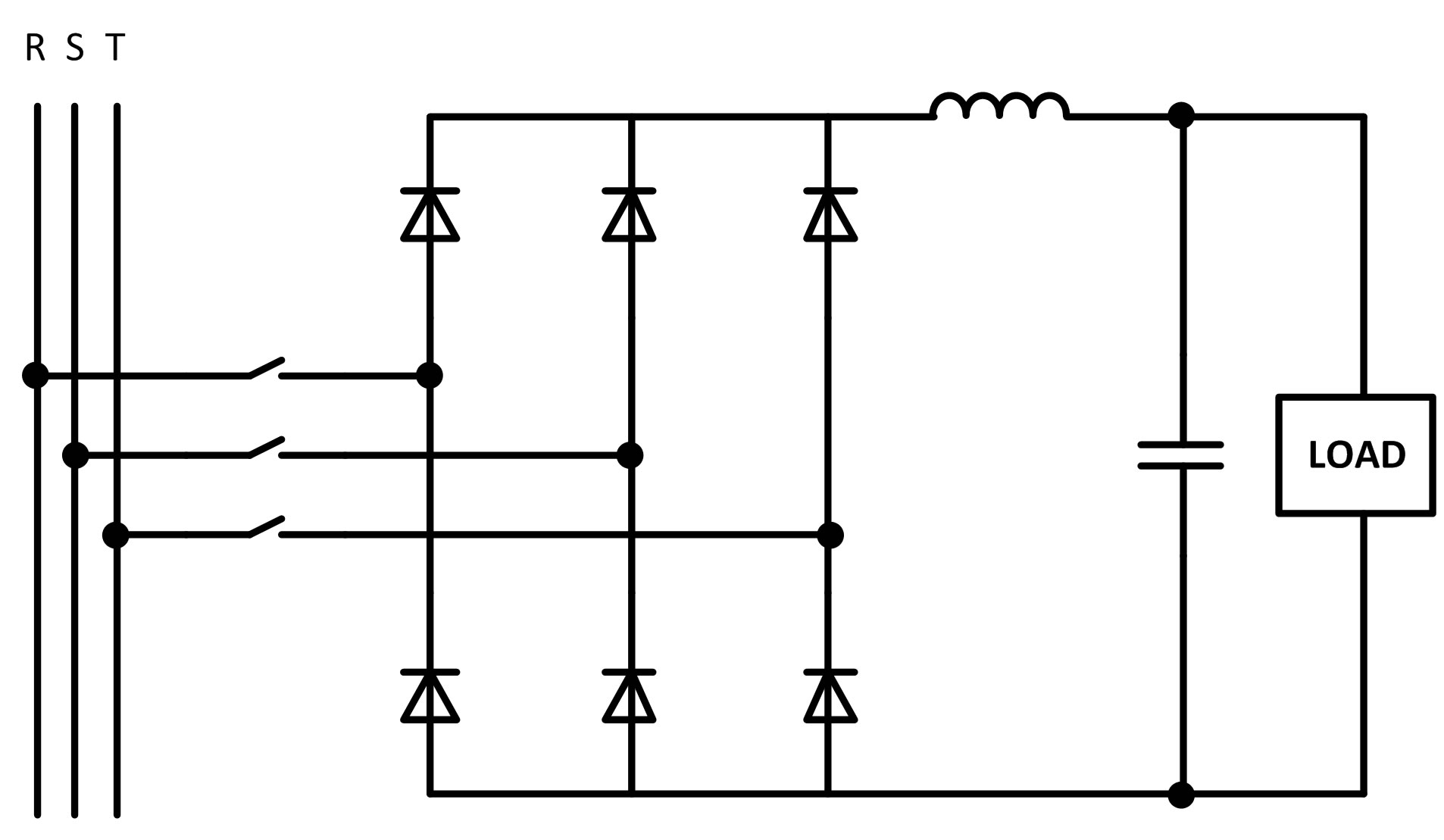
Figure 7. Fully controlled buck rectifier.
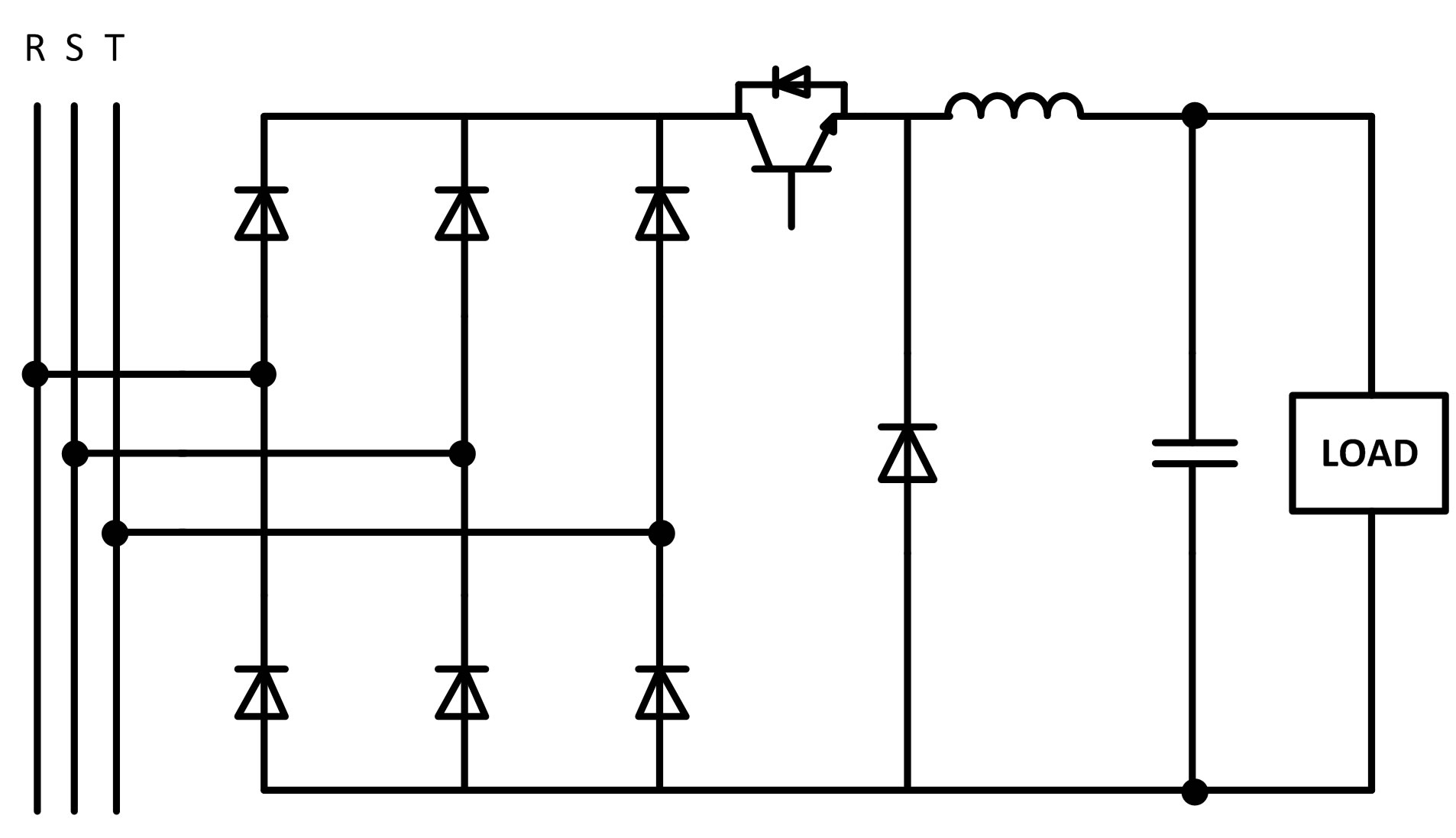
Figure 8. Single switch buck rectifier.
4) Series Active Filters [14]
This family of active filters is connected in series with the non-linear load, acting as a variable voltage source (Figure 10). The control method is usually a current control method, such as hysteresis control.
2.2. Topologies for Parallel Connection Schemes
2.2.1. Parallel Active Filter (PAF) [15-18]
The basic function of this topology is the injection of equal compensating currents (Figure 11), opposite in phase, to cancel harmonics and/or reactive components of the nonlinear load current at the point of connection. Many control methods have proposed in bibliography, such as direct power control, flux based control, P-I control, sliding mode control, etc.
2.2.2. Capacitor Mid-Point Four-Wire PAF [19,20]
This topology is a parallel active filter suitable for fourwire three phase loads (Figure 12). The dc-link consists of two capacitors connected in split. Thus the neutral point is connected directly to the midpoint of the dc-link capacitors.
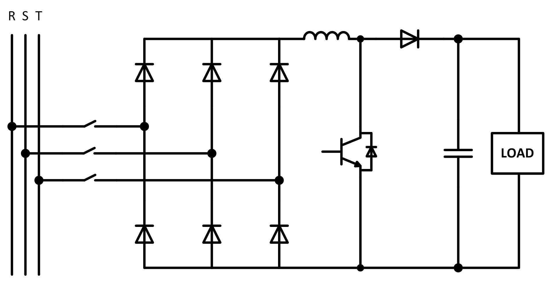
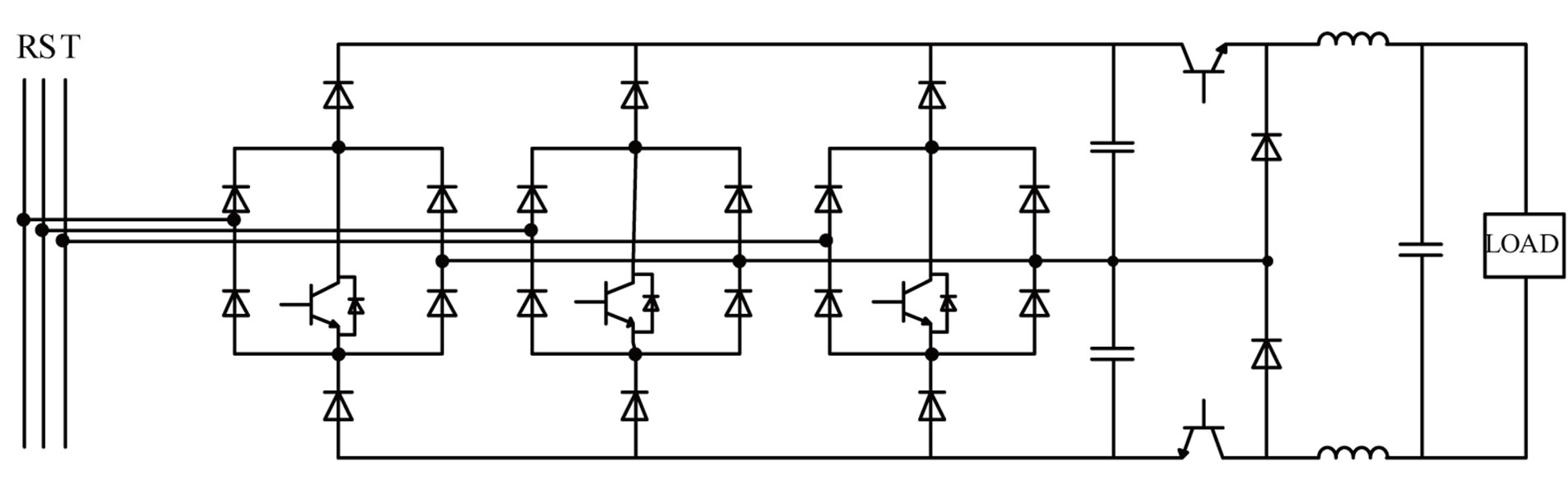
Figure 9. Buck-boost rectifiers.
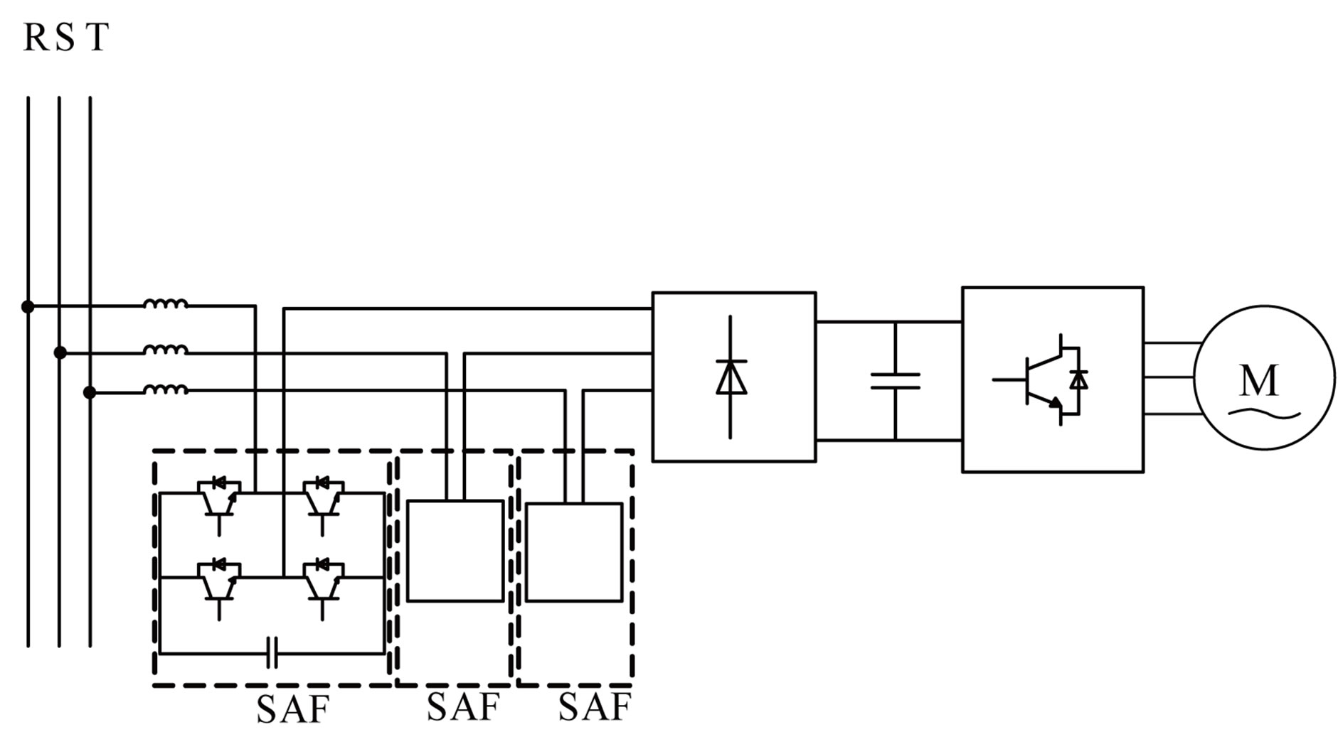
Figure 10. Series active filters.
2.2.3. Four-Pole Four-Wire PAF [21]
This is another variation of the parallel active filter for four-wire load, with an extra branch for the fourth wire (Figure 13).
3. Simulation of the above Topologies
All of the above mentioned topologies were simulated
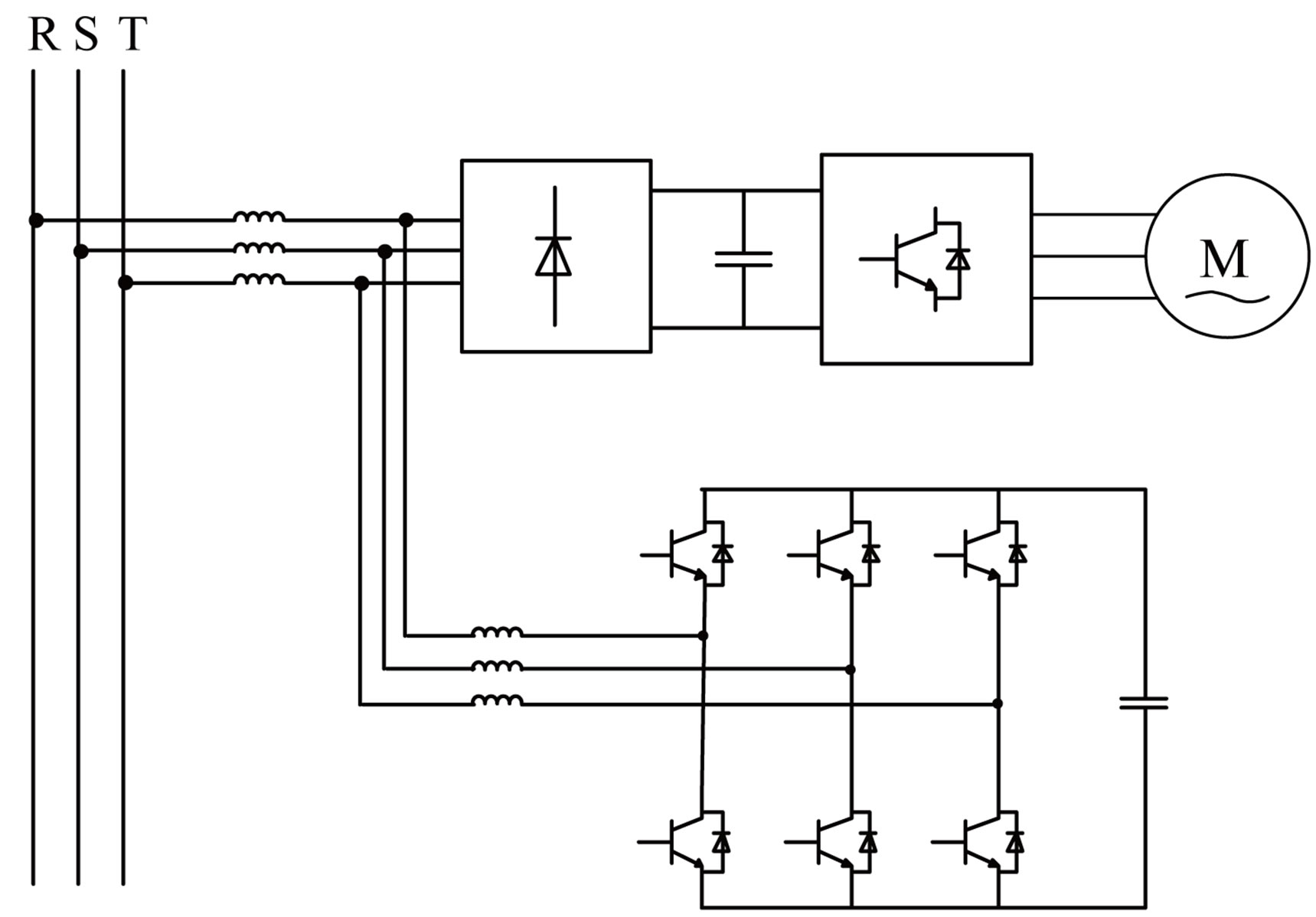
Figure 11. Parallel active filter.
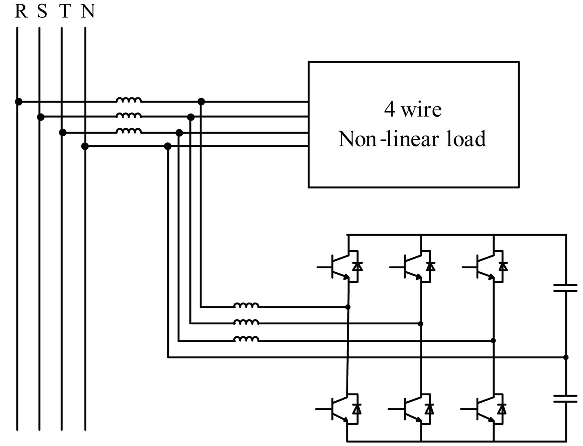
Figure 12. Capacitor Mid-Point active filter.
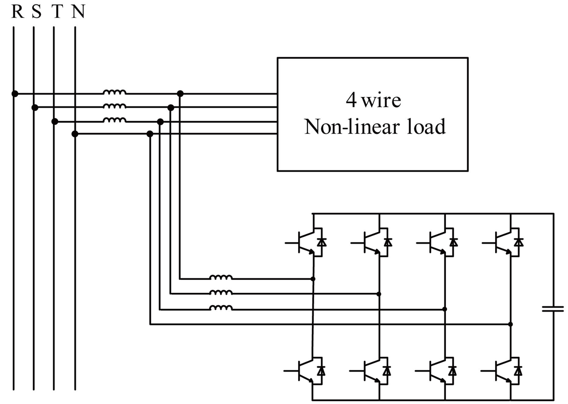
Figure 13. Four-pole four-wire parallel active filter.
using the SABER RD simulation tool. The SABER RD software is a powerful simulation suite that enables the simulation of electrical and mechanical systems. The use of detailed models for semiconductor devices and magnetic components allows the precise calculation of conductance and switching losses, as well as passive component losses (inductors, capacitors, etc.). Using the precise losses calculation, the efficiency as well as the power density (by calculating the coolant required) can be found. Figures 14-16 present some typical simulation results concerning voltage and current waveforms, for the cases of a buck rectifier and a single switch boost rectifier and for a 10 kW load level. Figure 14 demonstrates the simulation results for a semiconductor switch used on a buck rectifier. It can be clearly seen that the simulation tool can calculate conduction losses (while the switch is on) as well as switching losses (at the beginning and the end of conduction), thus the power dissipation estimation is adequately accurate. Figures 15 and 16 demonstrate the good pfc operation of the rectifiers under study.
It should be noted that an extended simulation process for all the converters under study has been conducted and the efficiency calculation took place for the case of a 10 kW load. This power level has been decided in order to cover the majority of industrial loads with a few parallel operating modules (1 - 5 modules).
4. Mass Analysis Procedure
The main parameters that determine mass/volume figures are the necessary cooling system and the passive elements of each converter (filter capacitors and inductors). The present analysis is based on the semiconductor losses calculation through the simulation results given for each converter. It is worth mentioning that the cooling system design for each converter stands for the safe operation of its semiconductor devices. As it concerns filter capacitors and inductors, their mass/volume has been based on commercial products which are in line with the
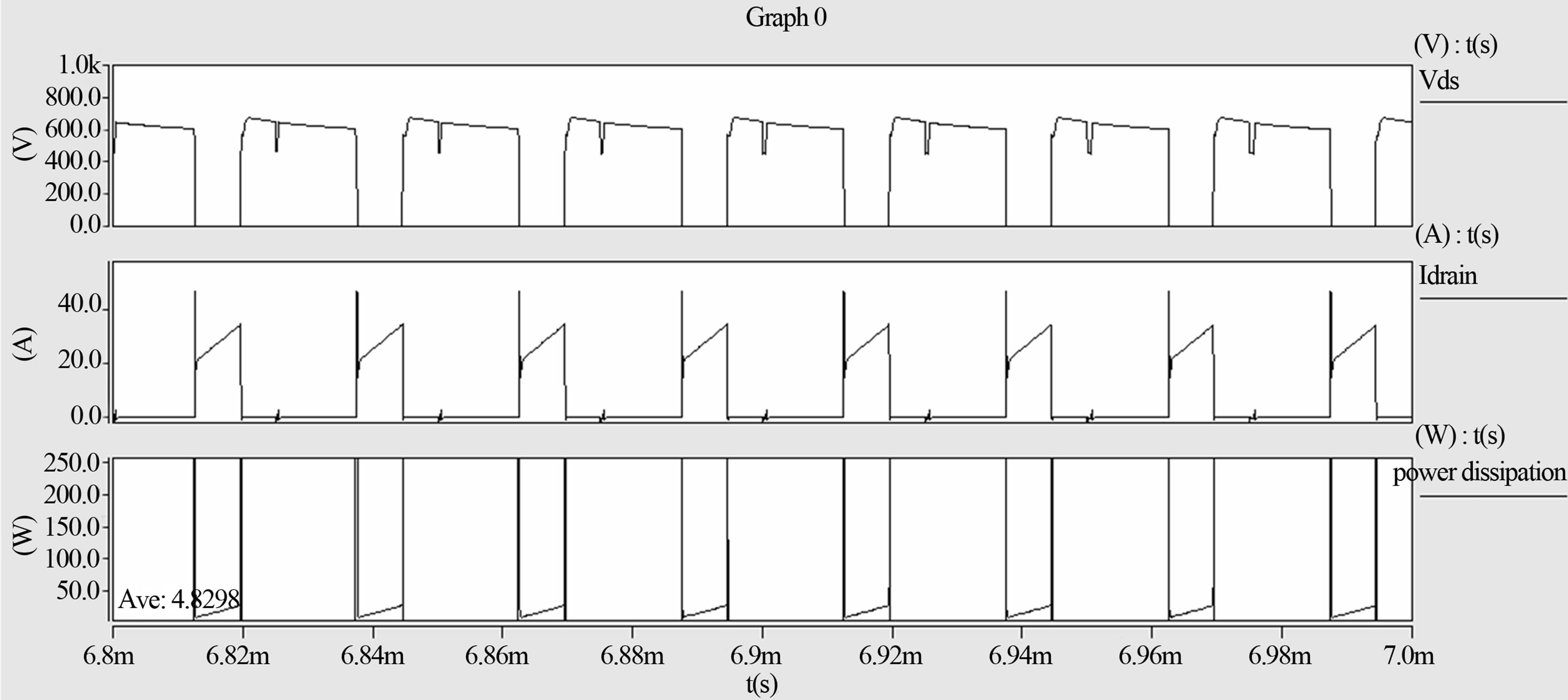
Figure 14. Drain-source voltage, drain current and power dissipation for a Mosfet used on a buck rectifier.
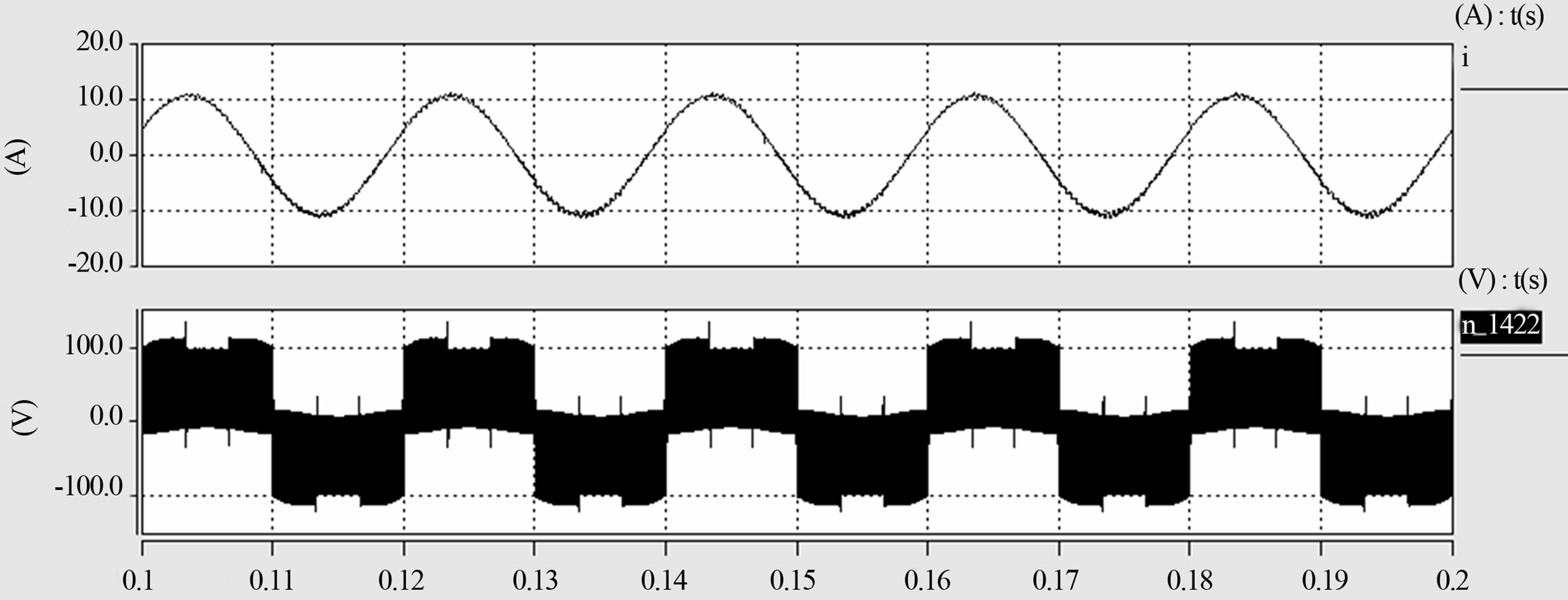
Figure 15. Input current of a buck rectifier unfiltered (lower case) and filtered (upper case).
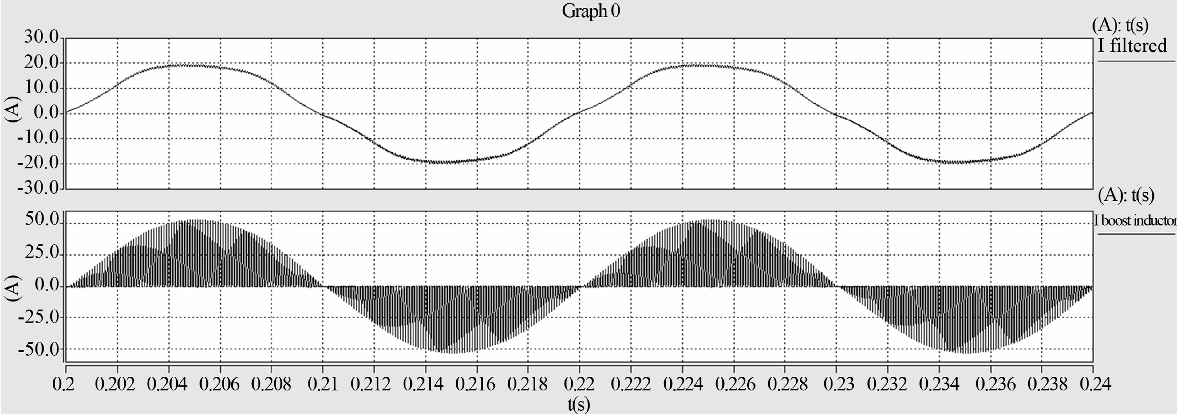
Figure 16. Input current of a single switch boost rectifier unfiltered (lower case) and filtered (upper case).
parameters’ values that have used in the simulation process.
Regarding the initial target values, the power density aim has been set to 3,0 kW/kg while the final product price aim has been set to 300 EUR/kW. The power density critical value has been set by some recent customer specifications (MILTECH HELLAS SA); the final product price target has been set in cooperation with engineers of many well-known Greek industries, in the context of a commercial survey conducted by our team. The focus on the Greek industries is justified by the fact that they constitute the initial target group for this project.
4.1. Thermal Design; Basic Principles
The cooling system design for each converter begins with the definition of the following parameters:
Maximum Junction Temperature, Tj
Ambient Temperature, Ta
Power dissipation (heat, due to power losses), q Then the following parameters are defined/calculated, according to the fundamental heat transfer calculations [22]:
Conduction Heat Transfer,
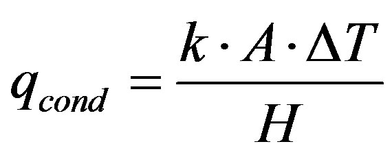 (3)
(3)
qcond, Heat flow due to conduction k, Thermal Conductivity A, Area normal to heat flow
ΔΤ, Temperature Difference H, Height in flow direction Conduction Thermal Resistance Rcond,
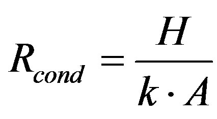 (4)
(4)
Convection Heat Transfer,
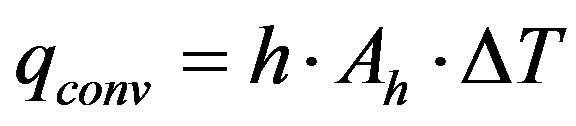 (5)
(5)
qconv, Heat flow due to convection h, Convection coefficient Ah, Area of convection
ΔΤ, Temperature Difference Convection Thermal Resistance, Rconv,
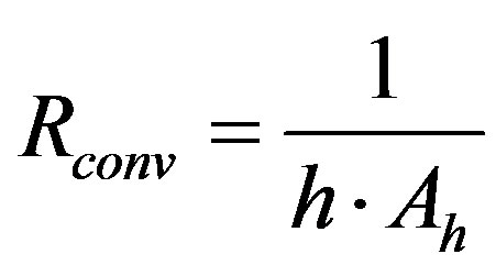 (6)
(6)
Total system thermal resistance, Rth,
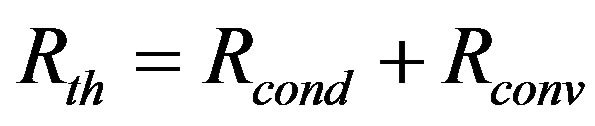 (7)
(7)
4.2. Finned Heat Sink Thermal Resistance Calculation
The finned heat sink layout is presented in Figure 17, assuming forced cooling due to forced air or forced water circulation; nevertheless, for the case under study (10 kW modules for industrial use) forced air circulation is more convenient and so this will be considered. The finned heat sink thermal resistance can be calculated by Equations (3)-(7), assuming an aluminum heat sink (for lighter and cost effective constructions); Rcond can be calculated directly by Equation (3) since the geometry of the heat sink is standardized and the aluminum thermal conductivity is equal to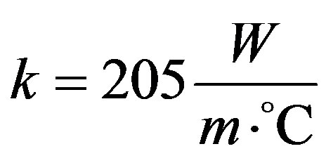 . As it concerns Rcovn Equation (6) can be rewritten as [22],
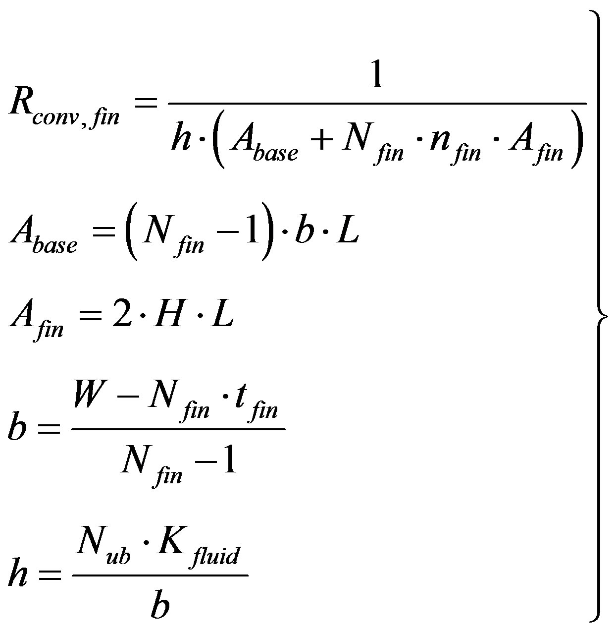 (8)
(8)
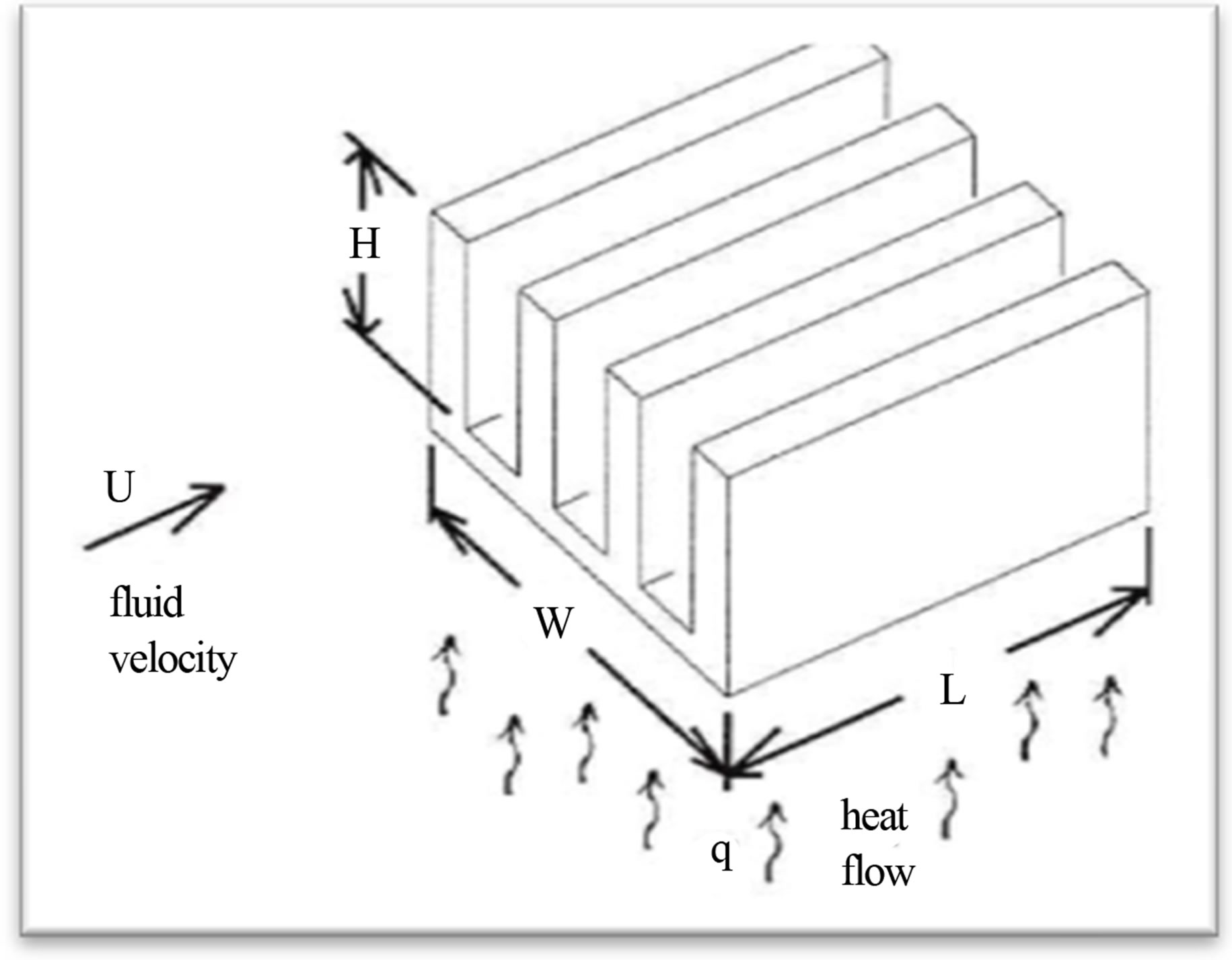
Figure 17. Finned heat sink thermal resistance calculation.
Rconv,fin, Finned heat sink convection thermal resistance Abase, Exposed surface area Afin, Heat transfer area Nfin, Number of fins nfin, Efficiency of Fins u, H, L, W, as in Figure 16
b, Gap between fins tfin, Fin width Kfluid, Thermal Conductivity of fluid (air for the specific application)
Nub, Nusselt Number (Function of Reynolds and Prandtl Numbers, which depends also on the finned heat sink structure Finally the fan selection (for forced air cooling) is based on the air pressure drop calculation, ΔP, as shown in Figure 18. Using the calculations of the thermal resistance and the pressure drop, the thermal design software tool used, comes up with the minimum geometric characteristics of the heat sink as well as the appropriate fan (among the ones that are registered in the relevant electronic library) that is needed in order to obtain a lower value than the power dissipation of the converter. The mass of the cooling system is calculated as a function of the geometric characteristics of the heat sink and its material, as well as the weight of the forced heat dissipation subsystem (if it is applied). A thermal design example for the converters under study is given in the following section.
4.3. Thermal Design Example
The previously presented thermal design procedure has been adopted by MILTECH HELLAS SA, for the development of its power converter products. In more details, a thermal design software tool has been developed, which calculates the necessary thermal management indexes (according to the customer settings) and comes up with the final cooling system setup. As an example, Figure 18 shows the converter setup while Table 1 shows the mass analysis details for the case of a 10 kW single switch boost PFC rectifier, according to MILTECH’s prototype tool. The converter efficiency (97%) has been calculated by simulating it with the SABER software. It is noted that this design procedure has been used for the mass estimation of all the studied converter topologies, as presented in the next section.
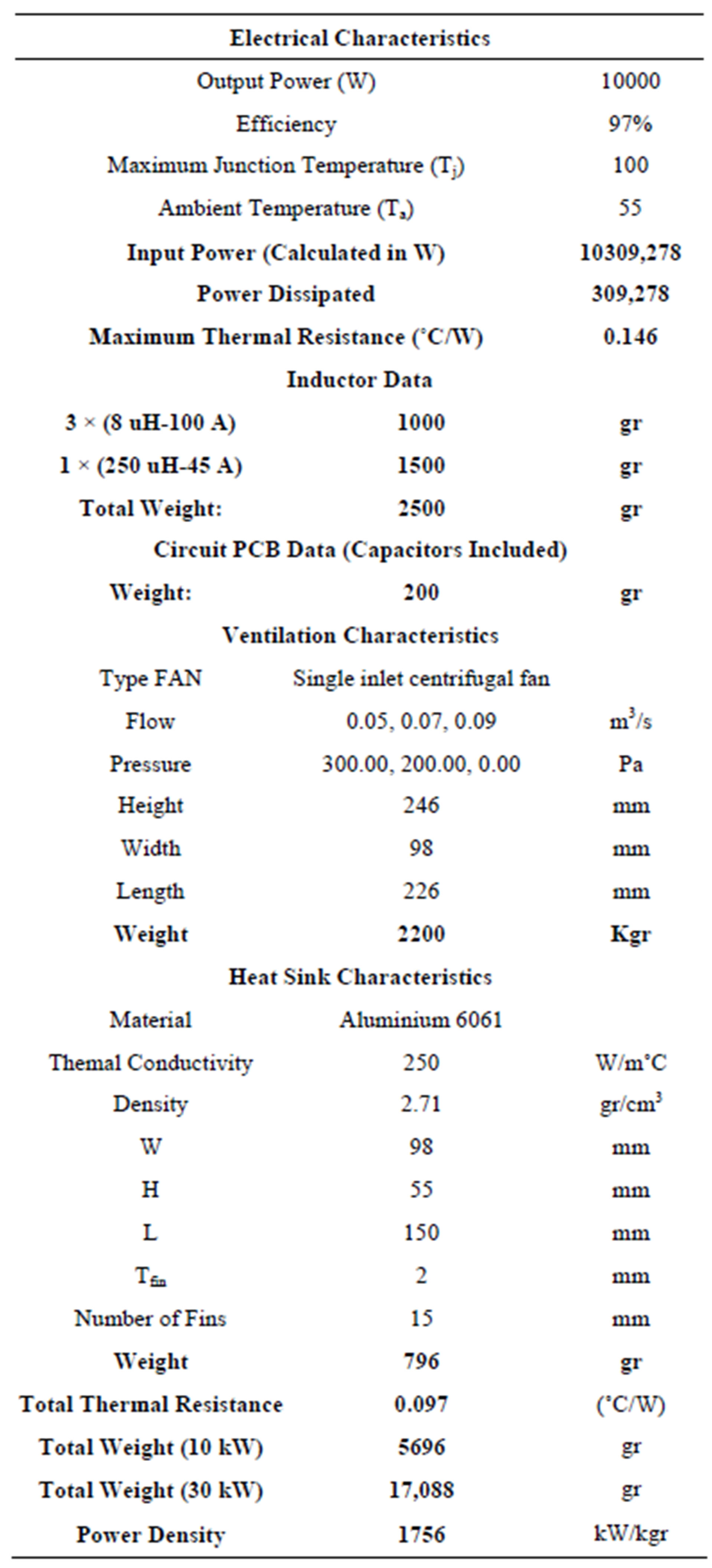
Table 1. Mass analysis for a 10 kW single switch boost PFC rectifier.
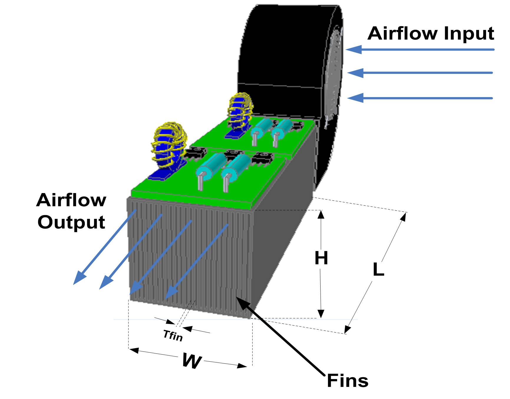
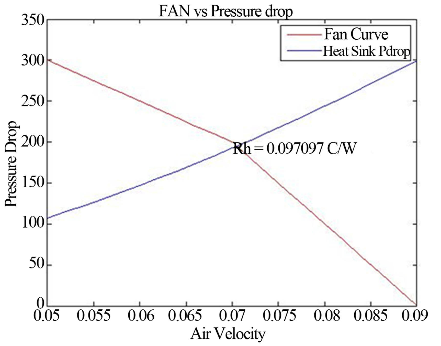
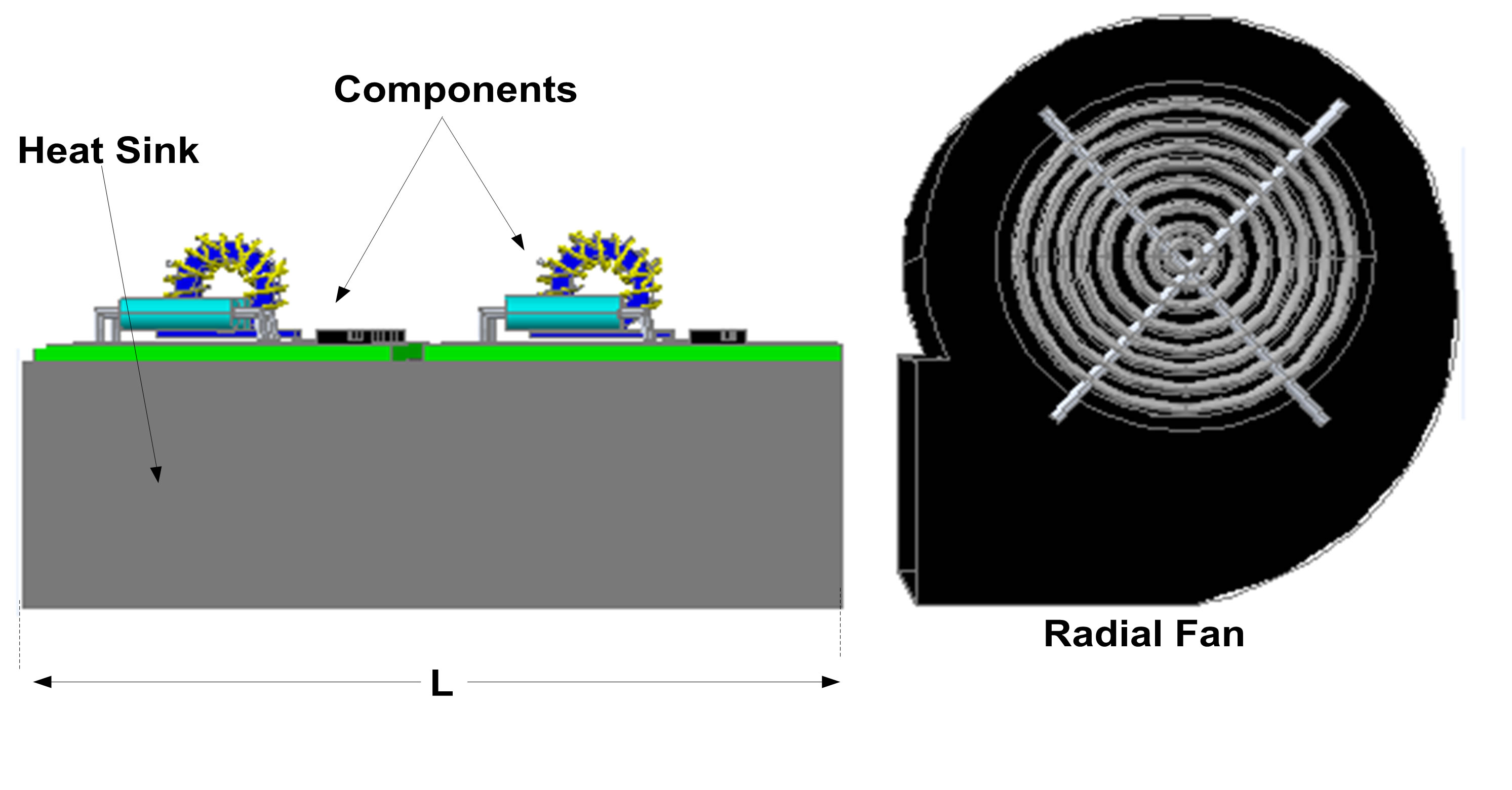
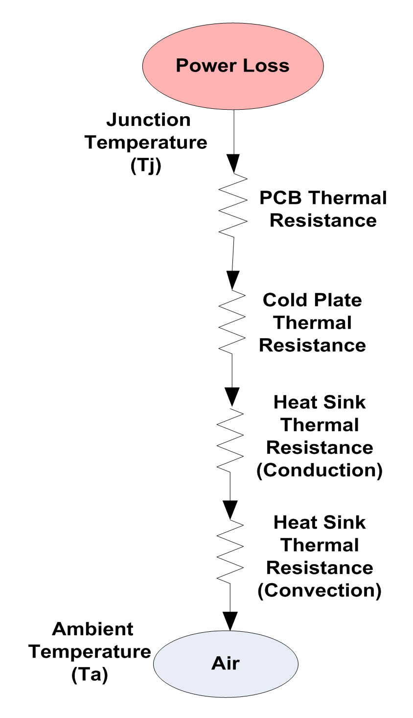
Figure 18. Thermal design example of a 10 kW single switch boost PFC converter.
5. Comparison of the Selected Topologies
A brief demonstration of the simulation as well as the mass/cost analysis results can be seen in Table 2, for all of the topologies under study. The simulations and the efficiency calculations were performed using the SABER software, as already discussed in Section 3, for a 10 kW load power and the criteria used for the evaluation of the topologies were cost related. Furthermore, final product price calculation has been done considering three years payback time for the manufacturing company. This is a very critical point due to the fact that the manufacturing company is an SME and so its resources are limited.
6. Conclusions
A detailed study of power factor correction topologies for industrial applications has been presented in this paper. The most appropriate converter topologies have been analyzed, simulated with SABER RD software and designed as industrial prototypes. The outcome results of the mass/cost analysis show that 3.0 kW/kg power density is a realistic target even without using expensive forced water cooling methods. It is noted that the power density aim of 3.0 kW/kg has been initiated by the electric vehicle and the aircraft industry and it is now a trend that is followed by the majority of the competitive converter manufacturers. However, the most prominent converter topology seems to be the Parallel Active Filter, since it demonstrates the maximum power density, while its expected product price is in the same range with the PFC rectifiers. It is noted that this result stands only for the case of industrial loads (supplied by the three phase low voltage network) and for 10 kW modules, mainly due to the fact that PAF topologies handle only the reactive power part of the industrial load. Nevertheless, it can be deduced that for lower power levels (e.g. PC-TV power supplies, electronic ballast) PFC rectifiers may become more competitive in terms of power density and cost. Additionally, this topology gives the flexibility to manufacture a modular product that can be used in existing industrial loads (parallel connection) and build up simply by adding multiple modules (the only limitation is an interconnection signal among the parallel modules in order to share the load reactive power). Finally, with re-
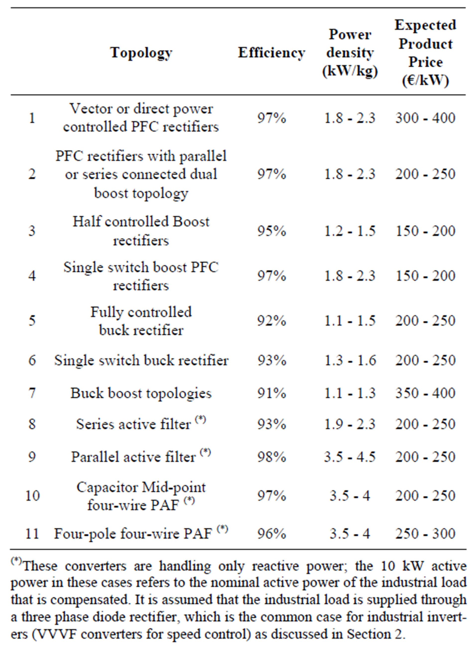
Table 2. Comparison of the above mentioned topologies.
gard to the expected final product price it has been proven to be competitive for the Greek industries—which are the initial target group of this project—according to a relevant commercial survey conducted by MILTECH.
Finally, as it concerns the future direction in the field of power factor correction topologies for industrial use, the most prominent target is the introduction of silicon carbide switches (both diodes and transistors); this may lead to substantial power losses reduction and conesquently to power density values higher than 5 kW/kg.
7. Acknowledgements
This work was supported by the “Reinforcement program of small and medium enterprises for research and technological development activities” under research project 23SMEs2009 and funded by the European social fund and by national funds.
REFERENCES
- J. L. Duarte, “Reference Frames Fit for Controlling PWM Rectifiers,” IEEE Transactions on Industrial Electronics, Vol. 46, No. 3, 1999, pp. 628-630. doi:10.1109/41.767071
- M. Malinowski, et al., “Virtual Flux Based Direct Power Control of Three-Phase PWM Rectifiers,” IEEE Transactions on Industry Applications, Vol. 37, No. 4, 2001, pp. 1019-1027. doi:10.1109/28.936392
- Q. Chongming and K. M. Smedley, “A General ThreePhase PFC Controller for Rectifiers with a Series-Connected Dual-Boost Topology,” IEEE Transactions on Industry Applications, Vol. 38, No. 1, 2002, pp. 137-148. doi:10.1109/28.980368
- Q. Chongming and K. M. Smedley, “A General ThreePhase PFC Controller for Rectifiers with a Parallel-Connected Dual Boost Topology,” IEEE Transactions on Power Electronics, Vol. 17, No. 6, 2002, pp. 925-934. doi:10.1109/TPEL.2002.805582
- J. C. Salmon, “Reliable 3-Phase PWM Boost Rectifiers Employing a Stacked Dual Boost Converter Subtopology,” IEEE Transactions on Industry Applications, Vol. 32, No. 3, 1996, pp. 542-551. doi:10.1109/28.502165
- J. Kikuchi, M. D. Manjrekar and T. A. Lipo, “Performance Improvement of Half Controlled Three-Phase PWM Boost Rectifier,” The 30th Annual IEEE of Power Electronics Specialists Conference (PESC 99), Vol. 1, Charleston, August 1999, pp. 319-324.
- A. R. Prasad, P. D. Ziogas and S. Manias, “An Active Power Factor Correction Technique for Three-Phase Diode Rectifiers,” IEEE Transactions on Power Electronics, Vol. 6, No. 1, 1991, pp. 83-92. doi:10.1109/63.65006
- N. Takeuchi, “A Novel PFC Circuit for Three-Phase Utilizing a Single Switching Device,” IEEE 30th International Telecommunications Energy Conference (INTELEC 2008), San Diego, 14-18 September 2008, pp. 1-5.
- Y. Nishida, “Three-Phase PWM-Current-Source Type PFC Rectifier (Theory and Practical Evaluation of 12kW Real Product),” Power Conversion Conference (PCC 2002), Vol. 3, Osaka, 2002, pp. 1217-1222.
- K. Wang, D. Boroyevich and F. C. Lee, “Charge Control of Three-Phase Buck PWM Rectifiers,” The 30th Annual IEEE of Applied Power Electronics Conference and Exposition (APEC 2000), Vol. 2, New Orleans, 2000, pp. 824- 831.
- J.-H. Song, et al., “A Pulse Frequency Modulation Control Method for Single-Switch Three-Phase Buck Rectifiers,” The 20th International Telecommunications Energy Conference, 1998, San Francisco, pp. 231-236.
- D. Bortis, et al., “25kW 3-Phase Unity Power Factor Buck Boost Rectifier with Wide Input and Output Range for Pulse Load Applications,” The 16th IEEE International Pulsed Power Conference, Albuquerque, 17-22 June 2007, pp. 1505-1508.
- T. Nussbaumer and J. W. Kolar, “Comparison of 3-Phase Wide Output Voltage Range PWM Rectifiers,” IEEE Transactions on Industrial Electronics, Vol. 54, No. 6, 2007, pp. 3422-3425. doi:10.1109/TIE.2007.896525
- Z. G. Pan, F. Z. Peng and S. L. Wang, “Power Factor Correction Using a Series Active Filter,” IEEE Transactions on Power Electronics, Vol. 20, No. 1, 2005, pp. 148-153. doi:10.1109/TPEL.2004.839819
- S. Saetieo, R. Devaraj and D. A. Torrey, “The Design and Implementation of a Three-Phase Active Power Filter Based on Sliding Mode Control,” IEEE Transactions on Industrial Applications, Vol. 31, No. 5, 1995, pp. 993- 1000. doi:10.1109/28.464511
- S. Bhattacharya, A. Veltman, D. M. Divan and R. D. Lorenz, “Flux-Based Active Filter Controller,” IEEE Transactions on Industrial Applications, Vol. 32, No. 3, 1996, pp. 491-502. doi:10.1109/28.502159
- S. Väliviita and S. J. Ovaska, “Delayless Method to Generate Current Reference for Active Filters,” IEEE Transactions on Industrial Electronics, Vol. 45, No. 4, 1998, pp. 559-567. doi:10.1109/41.704882
- A. Chandra, B. Singh, B. N. Singh and K. Al-Haddad, “An Improved Control Algorithm of Shunt Active Filter for Voltage Regulation, Harmonic Elimination, Power- Factor Correction, and Balancing of Nonlinear Loads,” IEEE Transactions on Power Electronics, Vol. 15, No. 3, 2000, pp. 495-507. doi:10.1109/63.844510
- B. Singh, K. Al-Haddad and A. Chandra, “A Review of Active Filters for Power Quality Improvement,” IEEE Transactions on Industrial Electronics, Vol. 46, No. 5, 1999, pp. 960-971. doi:10.1109/41.793345
- R. Griño, “Digital Repetitive Control of a Three-Phase Four-Wire Shunt Active Filter,” IEEE Transactions on Industrial Electronics, Vol. 54, No. 3, 2007, pp. 1495- 1503. doi:10.1109/TIE.2007.894790
- P. Salmeron and S. P. Litran, “A Control Strategy for Hybrid Power Filter to Compensate Four-Wires ThreePhase Systems,” IEEE Transactions on Power Electronics, Vol. 25, No. 7, 2010, pp. 1923-1931. doi:10.1109/TPEL.2010.2043687
- F. Incropera and D. DeWitt, “Fundamentals of Heat and Mass Transfer,” 6th Edition, J. Wiley & Sons, New York, 2007.