Communications and Network
Vol.2 No.1(2010), Article ID:1277,15 pages DOI:10.4236/cn.2010.21002
A Comparison Study of Input ESD Protection Schemes Utilizing NMOS, Thyristor, and Diode Devices
Electronic and Electrical Engineering Departmet, Hongik University, Jochiwon, Korea
E-mail: jychoi@hongik.ac.kr
Received October 20, 2009; accepted December 22, 2009
Keywords: ESD protection, HBM, NMOS, thyristor, diode, mixed-mode
ABSTRACT
For three fundamental input-protection schemes suitable for high-frequency CMOS ICs, which utilize protection devices such as NMOS transistors, thyristors, and diodes, we attempt an in-depth comparison on HBM ESD robustness in terms of lattice heating inside protection devices and peak voltages developed across gate oxides in input buffers, based on DC, mixed-mode transient, and AC analyses utilizing a 2-dimensional device simulator. For this purpose, we construct an equivalent circuit model of input HBM test environments for CMOS chips equipped with input ESD protection circuits, which allows mixed-mode tran-sient simulations for various HBM test modes. By executing mixed-mode simulations including up to six ac-tive protection devices in a circuit, we attempt a detailed analysis on the problems, which can occur in real tests. In the procedure, we suggest to a recipe to ease the bipolar trigger in the protection devices and figure out that oxide failure in internal circuits is determined by the peak voltage developed in the later stage of dis-charge, which corresponds to the junction breakdown voltage of the NMOS structure residing in the protec-tion devices. We explain strength and weakness of each protection scheme as an input ESD protection circuit for high-frequency ICs, and suggest valuable guidelines relating design of the protection devices and circuits.
1. Introduction
CMOS chips are more vulnerable to electrostatic discharge (ESD) due to the thin gate oxides used, and therefore protection devices such as NMOS transistors are required at input pads. A large size for the protection devices is needed to reduce discharge current density and thereby to protect them against thermal-related problems. However, using the large devices adds parasitic capacitances to the input nodes to generate other problems such as gain reduction and poor noise characteristics in highfrequency ICs [1].
To reduce the added parasitics, various techniques have been suggested [1–3]. However, basic approaches should be to reduce the size of protection devices by utilizing, for example, thyristors or forward-biased diodes [4,5].
In this paper, we introduce three fundamental ESD protection schemes utilizing NMOS transistors, thyristors, and diodes, which can be implemented into input pad structures of high-frequency CMOS ICs, assuming usage of standard CMOS processes. While there can be many variants of the fundamental protection schemes, it is worthwhile to carefully examine the mechanisms leading to device failures when using the fundamental protection schemes since it can provide valuable information in designing most of protection circuits. We analyze and compare in detail discharge characteristics of the three protection schemes for various discharge modes in input human-body model (HBM) tests. A 2-dimensional device simulator, together with a circuit simulator, is utilized as a tool for a comparative analysis. The analysis methodology utilizing a device simulator has been widely adopted with credibility [6,7] since it can provide valuable information relating the mechanisms leading to device failure, which may not be obtained by measurements.
In Section 2, we suggest three protection device structures, which will be utilized for the comparative analysis, and introduce device characteristics based on DC device simulations, which will be utilized to confirm the mixedmode simulation results analyzed in Section 4. In Section 3, we briefly explain discharge modes in HBM tests and introduce the input protection circuits utilizing each suggested protection device. In Section 4, we construct an equivalent circuit model of a CMOS chip equipped with input protection devices to simulate various input HBM test situations, and execute mixed-mode transient simulations on the circuits including up to six active protection devices. We figure out weak modes, and present in-depth analysis results on critical characteristics such as peak voltages developed across gate oxides in input buffers, locations of peak temperature inside protection devices, and so on. In Section 5, we introduce AC device simulation results to compare magnitudes of the added parasitics when the suggested protection circuits are adopted. In Section 6, considerations relating device design are discussed.
2. Protection Device Structures and DC Characteristics
Figure 1 shows the NMOS protection device structure assumed in this work. The scales of two axes are in micrometers. The structure represents a conventional protection device incorporating n+ source and drain ESD implants, which is implied by the relatively deep junctions. In order to alleviate drain-contact melting problems caused by lattice heating, the gate-drain contact spacing is chosen to be 3.5μm, which can be considered as ordinary. Table 1 summarizes the principal structure parameters. The n+ and p+ junctions shown in Figure 1 are assumed to have Gaussian doping profiles with about 1020cm-3 of peak concentration.
The p+ junctions located at the upper left/right corners represent diffusions for substrate ground contacts. A series resistor of 1 MWμm, which is not shown in Figure 1, is connected at the bottom substrate node considering the distributed resistances leading to the substrate contacts located far away.
DC simulations were performed using a 2-dimensional device simulator ATLAS [8]. All necessary physical models including an impact ionization model were considered in the simulations. The latticeheating model included joule heat, generation-recombination heat, and Peltier-Thomson heat. The source, the gate, and the substrate were grounded, and the drain bias was varied for simulation.
Figure 2 shows the simulated drain current vs. voltage characteristics of the NMOS transistor in Figure 1 in a semi-log scale. We confirmed that a leakage current through the weakly inverted MOS channel dominates when the drain voltage is below 5V. Increasing the drain voltage, a leakage current through the reverse-biased n+-drain/p-sub junction starts to dominate, and the junction breakdowns by avalanche when the drain voltage is increased above 9.3V.
A generated hole current by avalanche flows to the substrate terminal to increase the body potential. With a sufficient hole current flowing, the body potential near the source junction gets high enough to forward-bias the n+-source/p-sub junction triggering a parasitic lateral npn (source/body/drain) bipolar transistor. The source, the body, and the drain act as an emitter, a base, and a collector, respectively. Generation of holes around the drain junction is augmented due to impact ionization caused by
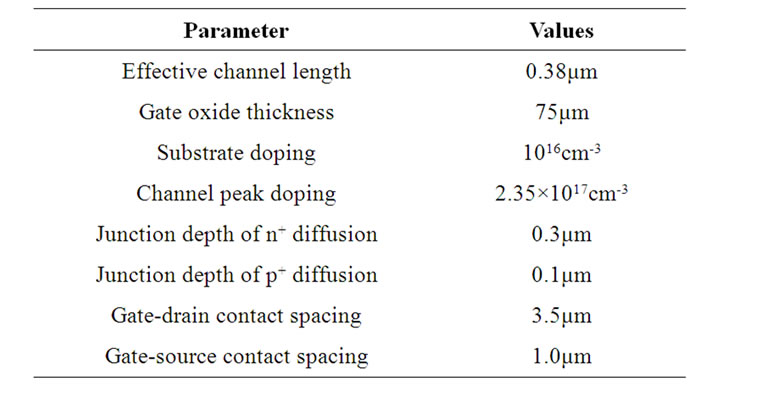
Table 1. Principal parameters of the NMOS device
Table 2. Principal parameters of the lvtr_thyristor device
the injected electrons from the source, and thereby the required drain-source voltage is reduced to show a snapback, as indicated as ‘BJT trigger’ in Figure 2. After the snapback at about 9.4V, the drain-source voltage drops to about 4.6V of a bipolar holding voltage.
In Figure 2, a 2nd breakdown [9] occurs when the drain current is about 1.3mA/μm, and the required drain-source voltage is further reduced to cause device failures relating drain-contact melting in real devices. It was confirmed that the 2nd breakdown in Figure 2 occurs when the peak lattice temperature inside the device exceeds about 1, 100°K.
Figure 3 shows the lvtr_thyristor device structure assumed in this work. An lvtr_thyristor device is a pnpntype device suggested to the lower snapback voltage by incorporating a NMOS transistor into it [4]. The device in Figure 3 can be easily fabricated in standard CMOS processes, and does not incorporate ESD implant steps, which is implied by the relatively shallow junctions.
Table 2 summarizes the principal structure parameters. The n well is assumed to have a Gaussian doping profile with 1017cm-3 of peak concentration, and the doping profiles of the n+ and p+ junctions are similar to those of the p+ junctions in Figure 1. A series resistor is also connected at the bottom substrate node as in the NMOS device in Figure 1. The n+ and p+ anodes in Figure 3 are tied together to serve as an anode. The cathode, the gate, and the substrate were grounded, and the anode bias was varied for simulation.
Figure 4 shows the simulated DC anode current vs. voltage characteristics of the lvtr_thyristor device in Figure 3. As in the NMOS device, when the drain voltage is below 5V, a leakage current through the weakly inverted MOS channel between the n+ well (the n+ region at the
Figure 1. Cross section of the NMOS device
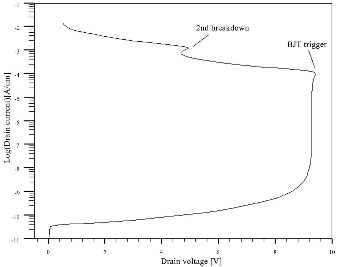
Figure 2. Drain I-V characteristics of the NMOS device
right-hand side of the n well) and the n+ cathode dominates. When increasing the drain voltage, a leakage current through the reverse-biased n+-well/p-sub junction, where electric field intensity is highest, starts to dominate, and the junction breakdowns by avalanche when the drain voltage is increased above 8.8V. The n+ well junction acts as a drain of the NMOS transistor, whose breakdown voltage is different from that of the NMOS
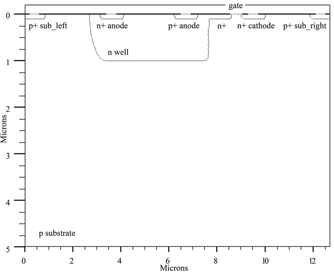
Figure 3. Cross section of the lvtr_thyristor device
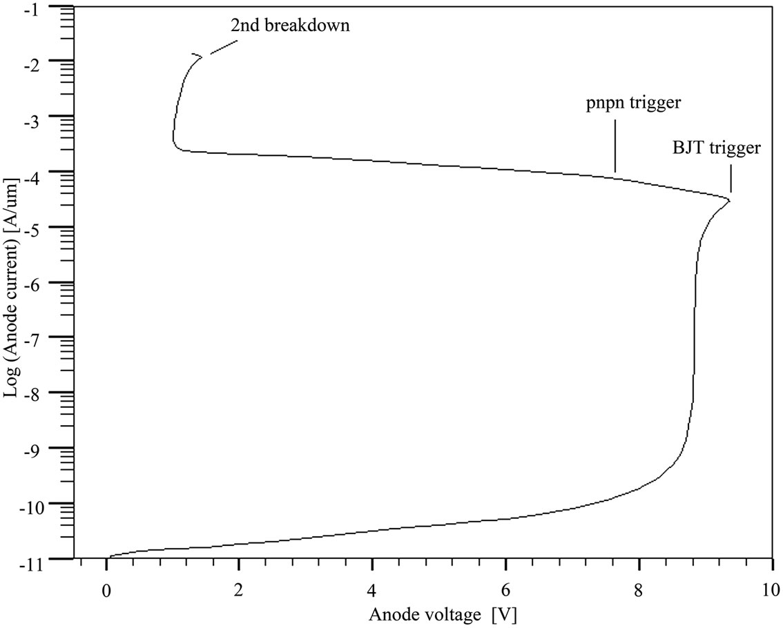
Figure 4. Anode I-V characteristics of the lvtr_thyristor device
device in Figure 1 due to the different junction-doping profile.
As the anode voltage increases, the p-sub/n+-cathode junction is forward biased triggering a lateral npn (n+-cathode/p-sub/n+-well) bipolar transistor. The n+ cathode, the p substrate, and the n+ well act as an emitter, a
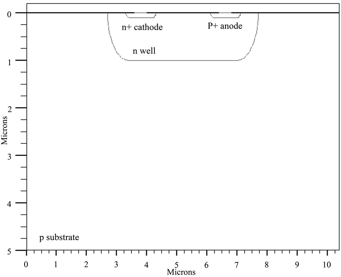
Figure 5. Cross section of the diode device
base, and a collector, respectively. At this situation, a snapback is monitored as shown in Figure 4. The collector current from the n+ anode flows through the n well to decrease the potential of the region under the p+ anode by an ohmic drop. When the collector current is large enough, the p+-anode/n-well junction is forward biased to trigger a pnpn (p+-anode/n-well/p-sub/n+-cathode) thyristor, which causes another decrease in the anode voltage, as indicated as ‘pnpn trigger’ in Figure 4. The resulting holding voltage drops to about 1V, which is much smaller compared to 4.6V of the NMOS transistor in Figure 2.
The 2nd breakdown in Figure 4 occurs when the anode current is about 12mA/μm. The critical current for the 2nd breakdown is much larger than that in the NMOS device due to the reduced holding voltage, which implies superior ESD robustness of the lvtr_thyristor device in suppressing lattice heating.
Figure 5 shows the diode device structure assumed in this work, which is a p+-anode/n-well/n+-cathode junction. The doping profiles of the n well, the n+ and p+ junctions are similar to those in the lvtr_thyristor device, and the contact spacing between the n+ cathode and the p+ anode was chosen as 2.4μm. The reason for forming the p+n junction inside the n well is to use the same device as a protection device between VDD and pad nodes as well as that between pad and VSS nodes. A series resistor is also connected at the bottom substrate node as in the NMOS device in Figure 1.
The substrate and the p+ anode were grounded and the n+ cathode bias was biased positively or negatively to simulate DC reverse-bias or forward-bias characteristics, respectively. From the DC simulation results, it was confirmed that the forward diode drop is 0.95V when the diode current is 0.2mA/μm, and the reverse breakdown voltage is about 11.3V.
3. Input ESD Protection
Since parasitics added to an input pad by adopting ESD protection circuits should be minimized, it is desired to connect fewer number of protection devices to an input pad. An effective way to reduce the number is to use a VDD-VSS clamp device since it provides discharge paths without adding parasitics to an input pad. Figure 6, 7 and 8 show the fundamental ESD protection schemes utilizing the assumed three protection devices while minimizing the added parasitics. In the figure, a CMOS inverter was assumed as an input buffer.
The NMOS device shown in Figure 1 is used for M1 and M2 in Figure 6. M1 is a protection device between the pad and VSS nodes, and M2 is a clamp device between the VDD and VSS nodes. It is important to locate all the protection devices close to the pad to minimize variation of the gate voltage in the input buffer when an ESD voltage is applied to the pad.
The lvtr_thyristor device shown in Figure 3 is used for T1 in Figure 7. The NMOS device shown in Figure 1 is used for M2. In T1, the p+ and n+ anodes are connected to
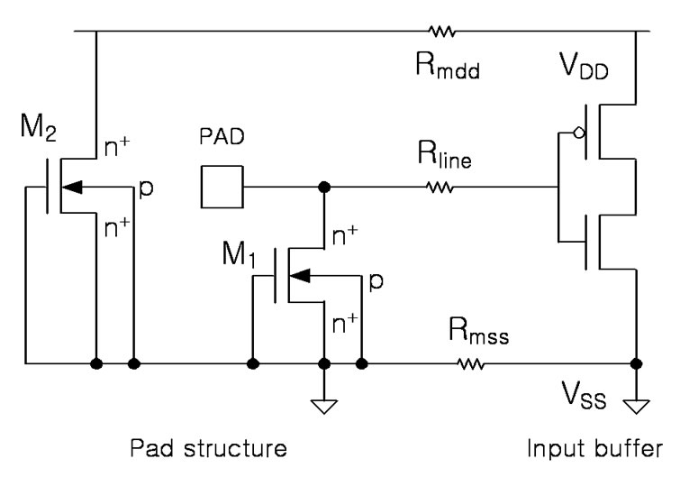
Figure 6. Protection scheme utilizing the NMOS device
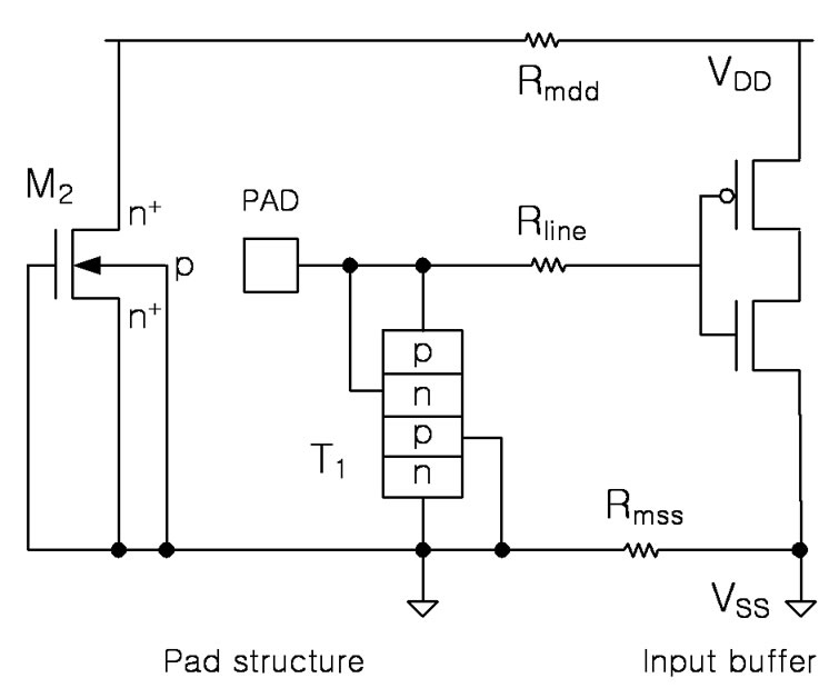
Figure 7. Protection scheme utilizing lvtr_thyristor device
the pad, and the p substrate and the n+ cathode are connected to VSS. Although it is not shown in Figure 7, the gate in T1 is also connected to VSS to maintain an off state in normal operations.
The diode device shown in Figure 5 is used for D1 and D2 in Figure 8. In D1, the n+ cathode is connected to the pad, and the p+ anode and the p substrate are connected to VSS. In D2, the n+ cathode, the p+ anode, and the p substrate are connected to VDD, the pad, and VSS, respectively.
Since HBM tests for input pins should include all possible discharge modes, tests are performed for the five modes defined below.
1) PS mode: +VESD at an input pin with a VSS pin grounded 2) NS mode: -VESD at an input pin with a VSS pin grounded 3) PD mode: +VESD at an input pin with a VDD pin grounded 4) ND mode: -VESD at an input pin with a VDD pin grounded 5) PTP mode: +VESD at one input pin with another input
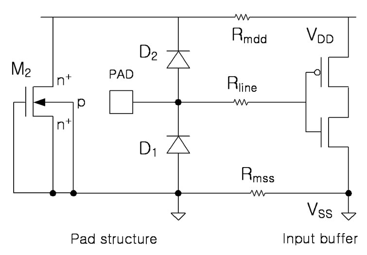
Figure 8. Protection scheme utilizing the diode devices
pin grounded
Figure 9 shows main discharge paths in the protection scheme utilizing the NMOS device. In a PS mode, a parasitic npn bipolar transistor in M1 provides a main discharge path, and in a NS mode, a forward-biased pn (p-sub/n+-drain) diode in M1 provides it. In a PD mode, a parasitic npn bipolar transistor in M1 and a forward-biased pn (p-sub/n+-drain) diode in M2 in series provides a main discharge path, and in an ND mode, a parasitic npn bipolar transistor in M2 and a forward-biased pn (p-sub/n+-drain) diode in M1 in series provides it.
Local lattice heating is proportional to a product of current density and electric field intensity, and therefore temperature-related problems in the protection devices can occur in the parasitic npn bipolar transistor rather than in the forward-biased diode since the holding voltage of the bipolar transistor is much larger. Therefore we should assign sufficient device widths to M1 considering PS and PD modes, and to M2 considering an ND mode.
Main discharge paths in the protection scheme utilizing the lvtr_thyristor device are almost same as those shown in Figure 9 except that discharge paths inside T1 replacethose in M1. That is, a pnpn thyristor in T1 performs the role of the parasitic npn bipolar transistor in M1, and a forward-biased pn (p-sub/n+-anode) diode in T1 performs the role of the forward-biased pn (p-sub/n+-drain) diode in M1.
Since lattice heating is not severe in pnpn thyristors by virtue of the smaller holding voltage, the width of the lvtr_thyristor device can be small. However, we should assign a sufficient device width to M2 considering an ND mode.
Figure 10 shows main discharge paths in the protection scheme utilizing the diode devices. In a PS mode, forward-biased D2 and an npn bipolar transistor in M2 in series provides a main discharge path, and in an NS mode, forward-biased D1 provides it. In a PD mode, forward-biased D2 provides a main discharge path, and in an ND mode, an npn bipolar transistor in M2 and forward-biased D1 in series provides it.
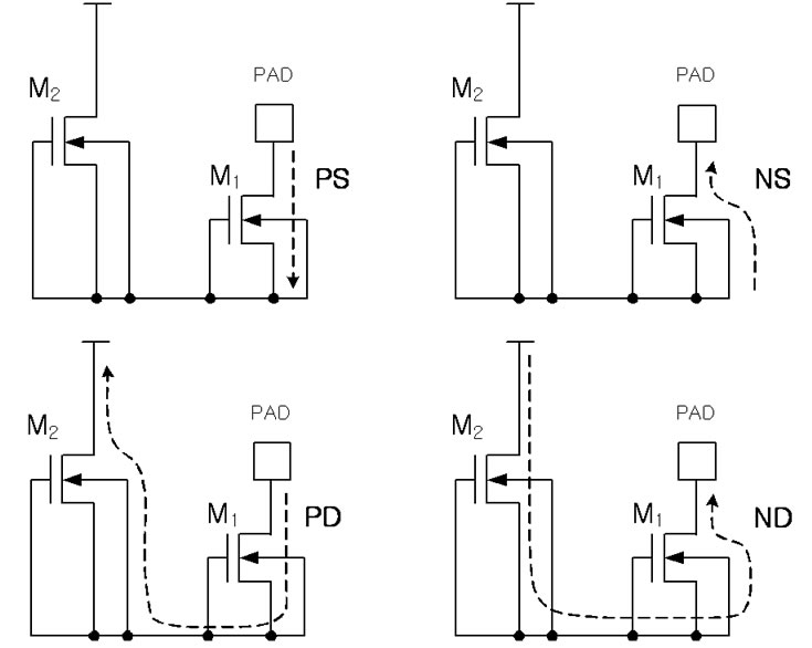
Figure 9. Main discharge paths in the protection scheme utilizing the NMOS device
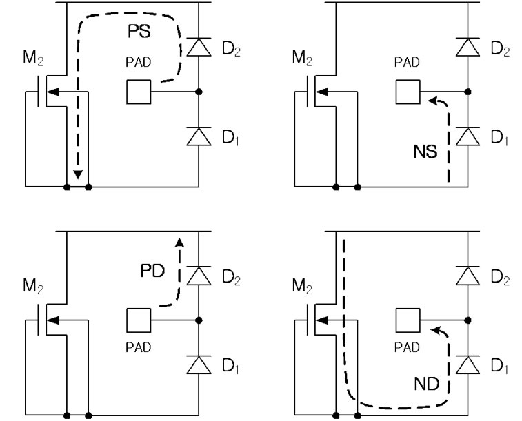
Figure 10. Main discharge paths in the protection scheme utilizing the diode devices
Since lattice heating is not severe in forward-biased diodes by virtue of the smaller voltage drop, the width of the diode devices can be small. However, we should assign a sufficient device width to M2 considering PS and ND modes.
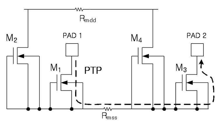
Figure 11 shows main discharge paths for a PTP mode. As shown on Figure 11(a), an npn bipolar transistor in M1 and a forward-biased pn (p-sub/n+-drain) diode in M3 in series provides a main discharge path in the protection scheme utilizing the NMOS device. It can be easily inferred that a pnpn thyristor in T1 and a forward-biased pn (p-sub/n+-anode) diode in T3 in series provides a main discharge path in the protection scheme utilizing the lvtr_thyristor device. As shown on Figure 11(b), two forward-biased pn (p+-anode/n+-cathode) diodes D2, D3 and an npn bipolar transistor in M4 in series provides a main discharge path in the protection scheme utilizing the diode devices.
 (a)
(a)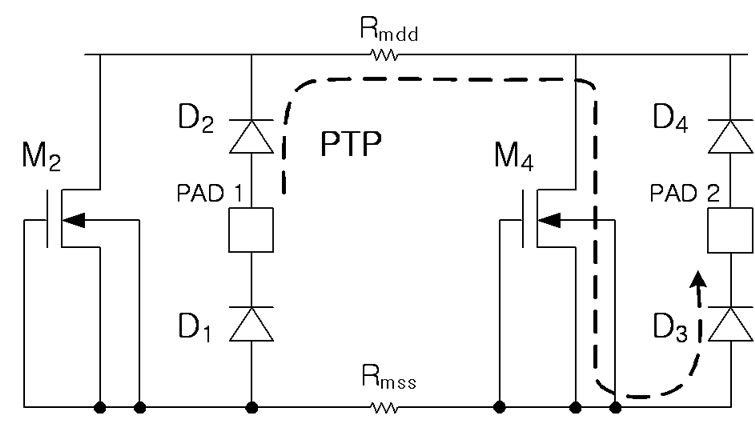 (b)
(b)
Figure 11. Main discharge paths for the PTP mode in the protection scheme utilizing (a) the NMOS device and (b) the diode devices
4. Mixed-Mode Transient Simulations
Figure 12 shows an equivalent circuit of an input HBM test situation assuming a PS mode. The portion indicated as ‘Test environment’ is an equivalent circuit for the test equipment connection. CESD and RESD represent a human capacitance and a human contact resistance, respectively, and 100pF and 1.5kΩ were assigned according to the international standard, respectively. Cs, Ct, and Ls, represent small parasitic elements present between test
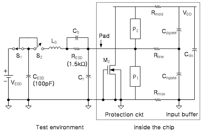
Figure 12. Equivalent circuit of an input-pin HBM test situation
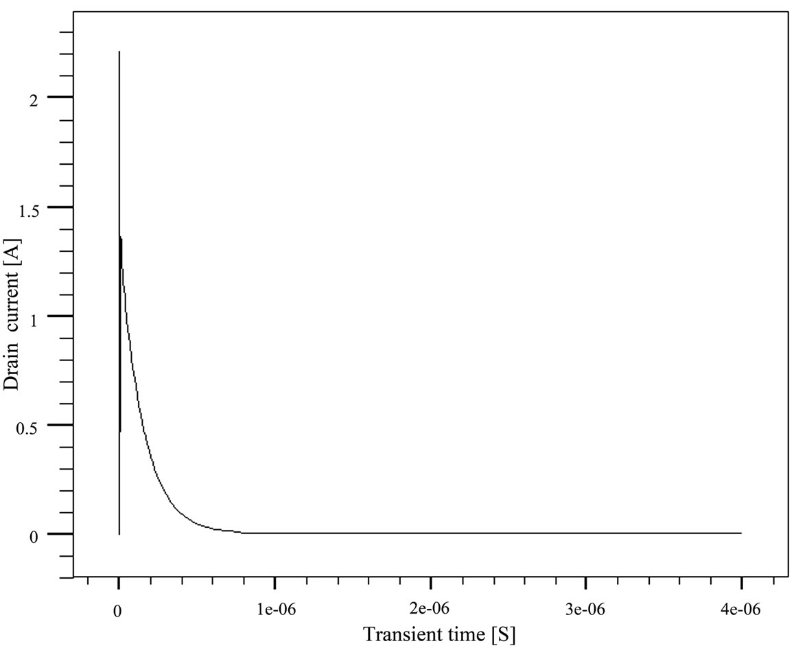
Figure 13. Variation of the drain current of M1 in a PS mode in case of using the NMOS protection circuit
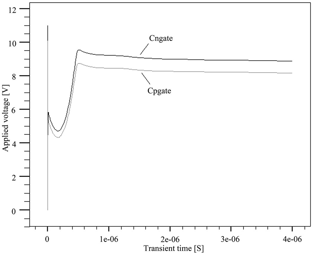
Figure 14. Variations of the voltages developed on Cngate and Cpgate in a PS mode in case of using the NMOS protection circuit
equipment and an input pad, and typical values of 1pF, 10pF, and 5μH [10] were assigned, respectively. VESD is a HBM test voltage, and the switch S1 charges CESD and then the switch S2 initiates discharge. By utilizing timevarying resistors for the switches, the switching times of S1 and S2 were set short as 0.15ns.
In Figure 12, a VDD-VSS clamp NMOS device M2, protection devices P1 and P2 form a representative protection circuit at an input pad. A CMOS inverter is assumed as an input buffer inside a chip, which is modeled by a capacitive network. Cngate and Cpgate represent gate oxide capacitances of an NMOS transistor and a PMOS transistor, respectively. Cds represents an n-well/p-sub junction capacitance. The reason for choosing this simple model for the inverter is based on the intension to minimize complexity of the equivalent circuit in this study focusing on the voltages developed across the gate oxides.
Rline, Rmdd, and Rmss represent metal-line resistances, whose values were assigned relatively small as 5Ω assuming an input buffer located close to an input pad to simulate a more critical situation.
Using ATLAS, we performed mixed-mode transient simulations utilizing the equivalent circuit in Figure 12 equipped with one of the three input protection circuits shown in Figures 6‑8. When a mixed-mode simulation is performed, active protection devices are solved by device and circuit simulations simultaneously. Notice that the number of the active protection devices included in a mixed-mode simulation in this work varies from two to six, which correspond to the PS, NS, PD, and ND mode simulations for the protection schemes in Figure 9, and the PTP mode simulation for the protection scheme util izing the diode devices in Figure 11(b), respectively.
For all the mixed-mode simulations performed for each test mode, VESD=±2000V was assumed. To make fair comparison on ESD robustness of the different protection schemes, the widths of the protection devices were adjusted to have utmost peak lattice temperature inside them below 500°K in all the mixed-mode simulations, resulting 250μm, 20μm, and 15μm for the NMOS device, the lvtr_thyristor device, and the diode device, respectively.
As an example of the mixed-mode simulation results, Figure 13 shows the variation of the M1 drain current as a function of time in a PS mode in case of using the NMOS protection circuit in Figure 6. Notice that M1 lies in the main discharge path in this case. The drain current reaches up to 2.2A, and shows a discharging characteristics with a time constant of roughly RESDCESD= 1.5kΩ ×100pF=0.15μs.
Figure 14 shows the variations of the voltages developed on the capacitors Cngate and Cpgate in the input buffer from the same simulation result. In Figure 14, the pad voltage is not shown since it is almost same with the voltage developed on Cngate.
In Figure 13 and 14, we can see that the parasitic bipolar transistor in M1 is triggered when the pad voltage in the early stage of discharge increases to about 11V, which is 0.68ns after S2 in Figure 12 is closed. Main discharge through the parasitic bipolar transistor proceeds as the pad voltage, which is equal to the drain-source voltage of M1, drops to the holding voltage of about 5V.
We can also see that the pad voltage increases again and reaches up to 9.5V at about 0.5μs, when the drain current is reduced below the holding current for the bipolar transistor action, and decreases very slowly thereafter. The peak voltage of 9.5V corresponds to the breakdown voltage of the NMOS device, which was explained relating Figure 2. The discharge thereafter continues a long time by the drain-junction leakage current in a breakdown mode. Up to 9.5V is developed on Cngate, and in overall a lower voltage by about 1V is developed on Cpgate since the VDD node does not lie in the main discharge path.
Since the discharge current decreases with time, the time for discharge to end is very long. We confirmed from additional simulations that it takes 7.4ms and 18.5 ms for the pad voltage to decrease down to 5V and 3V, respectively. If the pad voltage in the later stage of discharge is high, the NMOS gate oxide in the input buffer can be damaged since a large voltage is applied across it for a long time.
Figure 15 shows the variations of the voltages developed on Cngate and Cpgate in a PS mode in case of using the lvtr_thyristor protection circuit in Figure 7. We confirmed that the pad voltage is almost same with the voltage developed on Cngate again, and that the variation of the current through the anode of the lvtr_thyristor device T1 is similar to that in Figure 13.
In Figure 15, the parasitic bipolar transistor in T1 is triggered when the pad voltage in the early stage of discharge increases to about 12.8V, which is 0.77ns after S2 in Figure 12 is closed. Main discharge through the pnpn thyristor proceeds as the pad voltage, which is equal to the anode-cathode voltage of T1, drops to the holding voltage of about 2V.
We can also see that the pad voltage increases again and reaches to 6.5V at about 0.9μs, when the anode current is reduced below the holding current for the pnpn thyristor action, and decreases very slowly thereafter. We confirmed that main components of the anode current in this later stage of discharge are the leakage current through the n-well/p-sub junction and the weak-inversion MOS current. The developed voltage is smaller than the breakdown voltage (8.8V) of the lvtr_thyristor device shown in Figure 4. This seems to be caused by the longer duration (0.9μs) of the main discharge through the pnpn thyristor, compared to that (0.5μs) when using the NMOS protection scheme. The resulting discharge current in the later stage of discharge is too low for the lvtr_thyristor device to conduct in a breakdown mode.
We confirmed from additional simulations that it takes 165ms and 510ms for the pad voltage to decrease down to 5V and 3V, respectively.
In this case also, in overall a lower voltage by about 1V is developed on Cpgate since the VDD node does not lie in the main discharge path.
Figure 16 shows the variations of the voltages developed on Cngate and Cpgate as a function of time in a PS
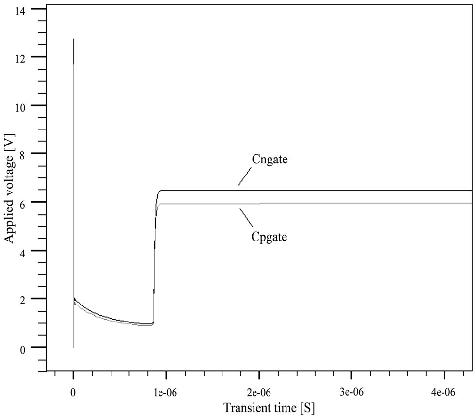
Figure 15. Variations of the voltages developed on Cngate and Cpgate in a PS mode in case of using the lvtr_thyristor protection circuit
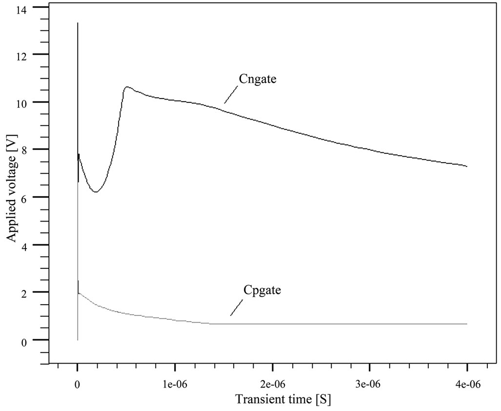
Figure 16. Variations of the voltages developed on Cngate and Cpgate in a PS mode in case of using the diode protection circuit
mode in case of using the diode protection circuit in Figure 8. We confirmed that variation of the anode current of D2, which lies in the main discharge path, is similar to that in Figure 13.
A forward-biased diode in D2 is triggered when the pad voltage in the early stage of discharge increases to about 13.4V, which is 0.82ns after S2 is closed. At this point the voltage developed across D2 in Figure 8 corresponds to about 7.6V. Main discharge through the forward-biased diode in D2 and the parasitic bipolar transistor in M2 in series proceeds when the pad voltage drops to a sum of the forward diode drop and the holding voltage, which is about 7V.
We can see that the pad voltage increases again and reaches to 10.7V at about 0.5μs when the drain current of the clamp NMOS device is reduced below the holding current for the bipolar transistor action. The peak voltage 10.7V corresponds to a sum of the forward diode drop in D2 (1.2V) and the breakdown voltage of M2 (9.5V). Therefore, the maximum voltage developed on Cngate is larger by an amount of the forward diode drop in D2 when compared with that in case of using the NMOS protection circuit.
In Figure 16, the voltage developed on Cpgate is maintained low all the time since it is almost equal to the forward diode drop in D2.
4.1 Voltages across the Gate Oxides in the Early Stage of Discharge
In case of the PS mode analyzed up to this point, the trigger times for the parasitic bipolar transistor in M1, the parasitic bipolar transistor in T1, and the forward diode in D2 are 0.68ns, 0.77ns, and 0.82ns, respectively, which are relatively short without big differences. However, due to these times, voltages larger than the snapback voltage or the ordinary forward diode drop appear across the devices right after S2 is closed, resulting the high voltages developed on Cngate in the early stage of discharge in Figures 14, 15 and 16.
Depending on test modes, larger peak voltages across the gate oxides appear at Cngate or Cpgate in the early stage of discharge. If we define the test modes, which produce larger peak voltages in the mixed-mode transient simulations performed for 5 test modes, as weak modes, the results can be summarized as shown in Table 3.
The peak voltages in Table 3 could be regarded as excessive; however, the durations of the peak voltages are very short. We confirmed that, for example, the durations for which the voltages exceed 10V are at most 0.3ns. Therefore it may be inferred that the gate oxides won’t be damaged in the early stage of discharge [11].
Notice that the peak voltages can be suppressed by reducing the bipolar trigger voltage of the NMOS protection device. To make the bipolar trigger voltages even lower than the off-state DC breakdown voltages, the gate-coupled NMOS (gcNMOS) structure [12] can be adopted. It is based on the technique to adding a RC network to the gate node, which is composed of a coupling capacitor (CC) connected between the gate and the drain nodes to turn on the NMOS transistor immediately after a positive ESD pulse is applied to the drain, and a resistor (RG) connected between the gate and VSS nodes to discharge the gate node thereafter. The on duration is defined by RGCC. Turning on the NMOS transistor reduces the bipolar trigger voltage with enhanced hole generation at a lower drain-source voltage.
It seems possible to obtain a similar result by simply
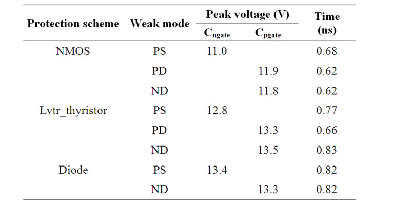
Table 3. Peak voltages developed across the gate oxides in the early stage of discharge
adding a series resistor between the gate and VSS nodes since the gate-drain overlap capacitance (Cgd) already exists in the NMOS structure, avoiding an increase of added parasitic to the input node. For the lvtr_thyristor device, the same technique may be applied since it includes the same NMOS structure in it.
We performed addition simulations to confirm that the early peaking can be suppressed by adding the series resistor to the gate node. For the 250μm NMOS device, adding a 10kΩ resistor between the gate and VSS nodes is enough to turn on the NMOS for about 5ns duration suppressing the peak voltage on Cngate down to 8.7V in case of the PS mode when using the NMOS protection scheme. The gate voltage peaks around 1.45V at 0.5ns, and the bipolar trigger time is also reduced to 0.5ns in accordance. Adding higher than a 50kΩ resistor turns on the NMOS transistor for an excessive duration more than 30ns, and tends to exacerbate lattice heating by confining the main discharge current towards the surface for a longer time.
When using the diode protection scheme, the same recipe on the NMOS clamp device suppresses the peak voltage down to 10.1V in the PS mode, which is still high due to the needed trigger voltage for the diode but lower than that (10.65V at 0.5μs) in the later stage of discharge.
In case of the lvtr_thyristor device, there exist an n-well resistance (RNW) between the n+ anode and the n+well junction, which tends to reduce the peak voltage developed at the gate node by the resistive division. For the 20μm lvtr_thyristor device, a 125kΩ resistor connected between the gate and VSS nodes, which is larger by the same ratio (12.5) of the device sizes, suppresses the peak voltage down to 8.7V. The gate voltage peaks only 1.1V at 0.65ns, however it is still enough to utilize the recipe.
4.2 Voltages across the Gate Oxides in the Later Stage of Discharge
Depending on test modes, larger peak voltages across the gate oxides also appears at Cngate or Cpgate in the later
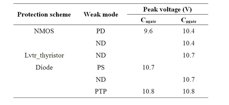
Table 4. Peak voltage developed across the gate oxides in the later stage of discharge stage of discharge. If we define the test modes, which produce larger peak voltages, as weak modes, the results can be summarized as shown in Table 4.
As explained relating the results in the PS mode, the high pad voltages in the later stage of discharge can damage the gate oxides since they last for long time.
In case of using the NMOS protection scheme in Table 4, the developed voltage on Cpgate in a PD mode is larger than that on Cngate since the forward diode drop in M2 is added to the breakdown voltage of M1, which can be easily explained from Figure 6 and 9. Due to the same reason, 10.4V is developed on Cpgate in an ND mode. In case of using the lvtr_thyristor protection scheme, 10.7V on Cpgate in an ND mode corresponds to a sum of the breakdown voltage of M2 and the forward diode drop in T1. The voltage is somewhat larger than that in the NMOS protection scheme since the diode drop in the lvtr_thyristor device is larger due to the smaller device width adopted. In case of using the diode protection scheme, the same voltage (10.7V) is developed on Cngate in a PS mode and on Cpgate in an ND mode, and this voltage corresponds to a sum of the breakdown voltage of M2 and the forward diode drop in D1 or D2. In a PTP mode, 10.8V is developed both on Cngate and Cpgate, which corresponds to a sum of the breakdown voltage of M4 and the forward diode drop in D2 or D3, which can be easily explained from Figures 8 and 11(b).
When judging from the peak voltages developed across the gate oxides in the later stage of discharge in Table 4, the weakest modes in case of using the NMOS protection scheme are PD and ND modes, and the PMOS gate oxide is more vulnerable to HBM ESD damages if the gate-oxide thicknesses of the NMOS and the PMOS are same. In case of using the lvtr_thyristor protection scheme, the weakest mode is an ND mode and the PMOS gate oxide is more vulnerable. In case of using the diode protection scheme, the weakest mode is a PTP mode and the NMOS and PMOS gate oxides are vulnerable in the same extent.
In Table 4, we can see that there is no big difference in the peak voltages developed across the gate oxides in the input buffers in each protection scheme. This is because the peak voltages in the later stage of discharge are determined mainly by the junction breakdown voltage of the NMOS structure in the NMOS devices or the lvtr_thyristor device. Since the breakdown voltage cannot be lowered with the gate coupling technique, junction engineering is essential to reduce it and to avoid possible oxide failures. We note that any junction engineering to lower the breakdown voltage was not tried in this work.
4.3 Location of Peak Temperature
As explained in Section 3, depending on test modes, utmost peak temperature resulting from lattice heating appears at the protection device connected to the input pad or at the VDD-VSS clamp NMOS device. In case of using the NMOS protection circuit, we confirmed that the utmost peak temperature in a PS mode appears at M1, which lies in the main discharge path, and Figure 17 shows the variation of the peak temperature inside M1. The peak temperature increases up to 495°K at about 30ns, when the bipolar transistor current still dominates the discharge, and decreases slowly as the discharge current decreases. By examining 2-dimensional temperature distributions, we confirmed that the peak temperature appears at the gate-side n+ drain junction.
In case of using the lvtr_thyristor protection circuit, the utmost peak temperature in a PS mode appears at T1, which lies in the main discharge path. The peak temperature inside T1, whose device width is set to 20μm, increases sharply up to 473°K at 0.9ns and decreases down to 330°K as the pnpn thyristor in T1 is triggered, and increases again up to 421°K at about 47ns, when the pnpn thyristor current still dominates the discharge, and decreases slowly. We confirmed that the peak temperature at 0.9ns appears at the n+ well junction, where the electric field is high in a breakdown mode, and that at 47ns appears at the n+ cathode junction, where the current density is high. Notice that the peaking at 0.9ns can be avoided by adopting the gate coupling technique to reduce the bipolar trigger voltage. With a 125kΩ resistor connected at the gate, the early peaking is reduced down to 370°K providing a room for reducing the device size by a small amount.
In case of using the diode protection circuit, the forward-biased D2 and the npn bipolar transistor in M2 in series provides a main discharge path in a PS mode, and the utmost peak temperature appears at M2. The peak temperature inside M2 increases up to 495°K at about 30ns, when the bipolar transistor current in M2 still dominates the discharge, and decreases slowly. We confirmed that the peak temperature appears again at the gate-side n+ drain junction. We also confirmed that the peak temperature inside D2, whose device width is set to 15μm, increases up to 485°K at about 45ns, and appears at the n+ cathode junction.
If we define the test modes, which produce larger tem-
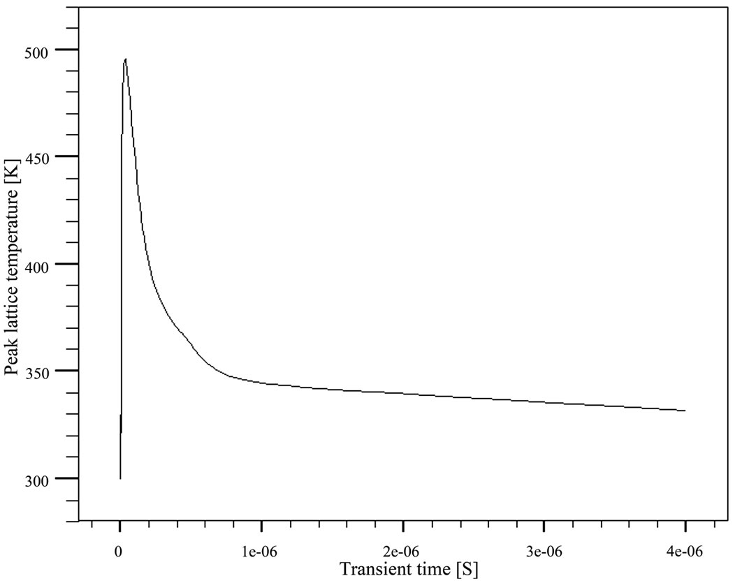
Figure 17. Peak temperature variation inside the NMOS device (M1) in a PS mode in case of using the NMOS protection circuit
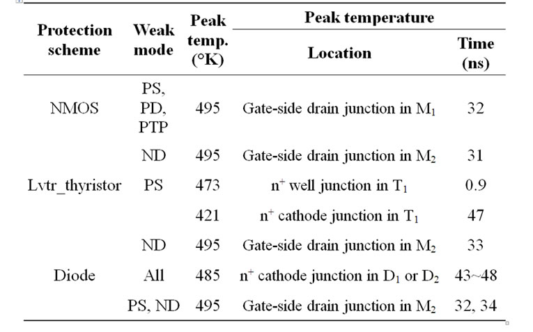
Table 5. Peak temperature locations and times
perature increase inside any protection device, as weak modes, the results can be summarized as shown in Table 5.
The peak temperature in the NMOS device, which is commonly used in all of the three protection circuits, appears at the gate-side n+ drain junction. This is the reason for assigning a large spacing between the gate and the drain contact in Figure 1 to avoid drain contact melting.
In case of using the lvtr_thyristor protection scheme, the peak temperature in T1 appears at the n+ well junction even though it can be avoided with the gate coupling technique. However, a problem with contact melting will not occur in this junction since there is no contact on it. The 2nd peak temperature in T1 appears at the n+ cathode junction, and junction engineering such as increasing the junction area or adopting ESD ion implantation may be required to restrain temperature increase. However, it will not add parasitics to the input pad since the junction is not connected to it.
In case of using the diode protection scheme, the peak temperature in D1 or D2 appears at the n+ cathode junction, and similar junction engineering may be required to restrain temperature increase. However, it will not add parasitics to the input pad unless the n-well size is increased since the junction stays inside the n-well.
5. AC Device Simulations
We performed AC device simulations using ATLAS to compare magnitudes of the parasitics added to an input pad when using three different protection schemes in Figures 6–8.
Since only the drain is connected to an input pad when using the NMOS device in Figure 1, all nodes except the drain were grounded and an AC voltage was applied to the drain for a simulation to get admittances of the device as a function of frequency. In case of the lvtr_thyristor device in Figure 3, all nodes except the n+ anode and the p+ anode were grounded and an AC voltage was applied to the anode. To get admittances of the diode device (D1) connected between the pad and the ground, all nodes except the n+ cathode were grounded and an AC voltage was applied to the n+ cathode. In case of the diode device (D2) connected between VDD and the pad, all nodes except the p+ anode were grounded and an AC voltage was applied to the p+ anode. The DC voltages for all nodes were assumed to be zero to simplify the analysis based on comparison.
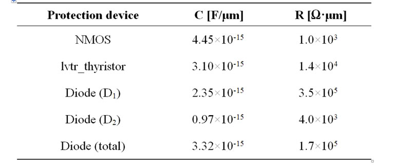
Table 6. Series R and C parasitics of the protection devices
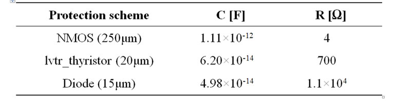
Table 7. Parasitics added to the input node in each protection scheme
Simple series RC circuits seem adequate as the AC equivalent circuits for the protection devices to roughly compare magnitudes of the added parasitics [13], and Table 6 summarizes the R and C values extracted by fitting the modeled admittances assuming series RC equivalent circuits to those by the AC device simulations. In Table 6, the diode (total) device denotes the parallel combination of D1 and D2.
Let’s focus on the capacitance values in Table 6. Main portion of the capacitance in the NMOS device is the n+-drain/p-sub junction capacitance, whose value is relatively large since the n+ junction is large and deep as shown in Figure 1. The main portion of the capacitance in the lvtr_thyristor device is a parallel sum of the n-well/psub junction capacitance and the n+ well/p-sub junction capacitance. While main portion of the capacitance in D1 is a parallel sum of the n-well/p-sub junction capacitance and the junction capacitance relating the p+ anode, that of the capacitance in D2 is the p+-anode/n-well junction capacitance alone. Fore this reason, the capacitance in D1 is larger than that in D2.
Table 7 summarizes the parasitics added to an input pad, computed from the simulated parasitics in Table 6 by considering the device widths in each protection scheme, which are shown in the parentheses. From Table 7, we can see that when using the protection circuit utilizing the lvtr_thyristor device or the diode device, the added parasitic capacitance to an input pad can be reduced to 1/18 or 1/22 of that when using the NMOS protection circuit, respectively, while providing a similar level of ESD robustness in terms of lattice heating. Therefore we can confirm that the lvtr_thyristor protection scheme and the diode protection scheme are much superior to the NMOS protection scheme if they are adopted as an input protection scheme in high-frequency ICs, for example, in RF ICs.
6. Design Considerations
6.1 Considerations in Designing the NMOS Device
By performing additional simulations, we figured out that a serious problem could occur when p-type substrate contacts are not located close to the NMOS device for the reason explained below.
When the p-sub/n+-drain forward diode in M1 or M2 in Figure 9 gets on in the early stage of discharge in PD, ND, and NS modes, the n+-source/p-sub junction is excessively reverse biased due to an ohmic drop inside the p-type substrate if substrate contacts are not located close. In that case, a parasitic npn (n+-drain/p-sub/n+-source) bipolar transistor inside the NMOS deice can be triggered to increase temperature around the n+ source junction a lot, where electric field intensity is high. By the same mechanism, in PD and ND modes, a sum of the bipolar holding voltages of M1 and M2, which is about 12V, is developed on Cpgate in a significant duration, which may damage the gate oxide. Therefore it is very important to locate the p-sub contacts close as shown in Figure 1.
6.2 Considerations in Designing the Lvtr_Thyristor Device
When p-type substrate contacts are not located close to the lvtr_thyristor device, the same problem with that in the NMOS device can occur in the lvtr_thyristor device. When the p-sub/n+-anode forward diode in T1 in Figure 7 gets on in the early stage of discharge in NS and ND modes, a parasitic npn (n+-anode/p-sub/n+-cathode) bipolar transistor inside the lvtr_thyristor deice can be triggered to increase temperature around the n+ cathode junction a lot, where electric field intensity is high. By the same mechanism, in an ND mode, a sum of the bipolar holding voltages of T1 and M2 is developed on Cpgate in a significant duration, which may damage the gate oxide. Therefore it is also very important to locate the p-sub contacts close as shown in Figure 3.
6.3 Considerations in Designing the Diode Device
The diode device in Figure 5 does not have p-type substrate contacts close to it. By performing additional simulations, we figured out that a serious problem can occur in a PS mode if p-type substrate contacts are located close.
Let’s assume that we attempt a PS mode test with an additional grounded p+-sub contact located at the upper right-hand side corner of the diode device in Figure 5. When the p+-anode/n+-cathode diode in D2 in Figure 10 gets on, a lateral parasitic pnp (p+- anode/n-well/ righthand side p+-sub) bipolar transistor inside D2 can be triggered to allow a large current and to increase temperature around the additional p+-sub contact a lot. We confirmed that even with the proposed diode structure in Figure 5, a vertical pnp (p+-anode/n-well/p-sub) in D2 is triggered. However, due to a resistance leading to p-sub contacts, amount of the bipolar current is restrained not to cause a temperature-related problem. Therefore it is very important to locate p-sub contacts as far away as possible.
6.4 Location of the Clamp NMOS Device
Since the clamp devices M2 in Figures 6–8 are large and consume a large area if they are located in every input pad, we may consider locating them between VDD and VSS buses in VDD and/or VSS pad structures. Although a clamp device M2 in that case can provide the same discharge paths explained, the ohmic voltage drops in the VDD and/or VSS bus with a very large discharge current flowing will increase the developed voltages across the gate oxides in input buffers, especially in case of adopting the diode protection circuit in Figure 8 since the ohmic voltage drops occur in both buses. Therefore it is recommended to locate M2 in each input pad structure unless the chip size is not a critical issue.
7. Summary
For three fundamental input-protection schemes suitable for high-frequency CMOS ICs, which utilize protection devices such as NMOS transistors, thyristors, and diodes, we attempted an in-depth comparison on HBM ESD characteristics based on DC, mixed-mode transient, and AC analyses utilizing a 2-dimensional device simulator.
For this purpose, we construct an equivalent circuit model of input HBM test environments for CMOS chips equipped with input ESD protection circuits, which allows mixed-mode transient simulations for various HBM test modes. By executing mixed-mode simulations including up to six active protection devices in a circuit and analyzing the results, we attempted a detailed analysis on the problems, which can occur in real tests. Contributions of this work can be summarized as follows.
1) We demonstrated a simulation-based method to analyze problems occurring in all possible input HBM ESD test modes.
2) We figured out weak modes in terms of the peak voltages developed across gate oxides in input buffers in each protection scheme. We showed that the voltage peaking in the early stage of discharge can be suppressed by simply adding a series resistor to the NMOS gate, and figured out that oxide failure is determined by the peak voltage developed in the later stage of discharge, which corresponds to the junction breakdown voltage of the NMOS structure residing in the protection devices.
3) We figured out weak modes in terms of temperature increase inside the protection devices in each protection scheme, and also figured out the locations of peak temperature inside the protection devices.
4) We compared magnitudes of the added parasitics to an input pad in each protection scheme to confirm that the lvtr_thyristor and the diode protection schemes are more suitable for highfrequency ICs.
5) We also suggested the valuable design guidelines to minimize temperature increase inside the protection devices and to minimize the voltages developed across the gate oxides in input buffers.
REFERENCES
- P. Leroux and M. Steyaert, “High-performance 5.2GHz LNA with on-chip inductor to provide ESD protection,” Electronics Letters, Vol. 37, pp. 467–469, March 2001.
- B. Kleveland, T. J. Maloney, I. Morgan, L. Madden, T. H. Lee, and S. S. Wong, “Distributed ESD protection for high-speed integrated circuits,” IEEE Transactions on Electron Devices, Vol. 21, pp. 390–392, August 2000.
- S. Hyvonen, S. Joshi, and E. Rosenbaum, “Cancellation technique to provide ESD protection for multi-GHz RF inputs,” Electronic Letters, Vol. 39, No. 3, pp. 284–286, February 2003.
- A. Chatterjee and T. Polgreen, “A low-voltage triggering SCR for on-chip ESD protection at output and input pads,” IEEE Electron Device Letters, Vol. 12, pp. 21–22, August 1991.
- E. R. Worley, R. Gupta, B. Jones, R. Kjar, C. Nguyen, and M. Tennyson, “Sub-micron chip ESD protection schemes which avoid avalanching junctions,” in Processing, EOS/ ESD Symposium, pp. 13–20, 1995.
- H. Feng, G. Chen, R. Zhan, Q. Wu, X. Guan, H. Xie, and A. Z. H. Wang, “A mixed-mode ESD protection circuit simulation-design methodology,” IEEE Journal SoilidState Circuits, Vol. 38, pp. 995–1006, June 2003.
- B. Fankhauser and B. Deutschmann, “Using device simulations to optimize ESD protection circuits”, in Processing, IEEE EMC Symposium, pp. 963–968, 2004.
- ATLAS II Framework, Version 5.10.2.R, Silvaco International, 2005.
- A. Amerasekera, L. van Roozendaal, J. Bruines, and F. Kuper, “Characterization and modeling of second breakdown in nMOST’s for extraction and ESD-related process and design parameters,” IEEE Transactions on Electron Devices, Vol. 38, pp. 2161–2168, September 1991.
- C. H. Diaz, S. M. Kang, and C. Duvvury, “Modeling of electrical overstress in integrated circuit,” Kluwer Academic Publishers, 1995.
- Z. H. Liu, E. Rosenbaum, P. K. Ko, C. Hu, Y. C. Cheng, C. G. Sodini, B. J. Gross, and T. P. Ma, “A comparative study of the effect of dynamic stressing on high-field endurance and stability of reoxidized-nitrided, fluorinated and conventional oxides,” in IEDM Technology Digest, pp. 723–726, 1991.
- G. Chen, H. Fang, and A. Wang, “A systematic study of ESD protection structures for RF ICs,” in Processing, IEEE Radio Frequency Integrated Circuit Symposium, Vol. 46, pp. 347–350, 2003.
- J. Y. Choi, “AC modeling of the ggNMOS ESD protection device,” ETRI Journal, Vol. 27, No. 5, pp. 628–634, October 2005.
NOTES
This work was supported by 2008 Hongik University Research Fund.