Natural Resources
Vol.4 No.3(2013), Article ID:33599,11 pages DOI:10.4236/nr.2013.43030
Modeling Multiple Quantum Well and Superlattice Solar Cells
![]()
1Department of Physics, University of Pinar del Río, Pinar del Río, Cuba; 2Solar Cell Laboratory, Institute of Materials Science and Technology (IMRE), University of Havana, Havana, Cuba; 3Higher School in Physics and Mathematics, National Polytechnic Institute, Mexico City, Mexico; 4Academic Unit of Physics, Autonomous University of Zacatecas, Zacatecas, México; 5Faculty of Physics, University of Havana, La Habana, Cuba; 6Nanophotonics Technology Center, Universidad Politécnica de Valencia, Valencia, Spain.
Email: dacs10@yahoo.com.mx
Copyright © 2013 Carlos I. Cabrera et al. This is an open access article distributed under the Creative Commons Attribution License, which permits unrestricted use, distribution, and reproduction in any medium, provided the original work is properly cited.
Received January 23rd, 2013; revised May 14th, 2013; accepted May 27th, 2013
Keywords: Quantum Well; Strain in Solids; Solar Cell; Conversion Efficiency; Modeling
ABSTRACT
The inability of a single-gap solar cell to absorb energies less than the band-gap energy is one of the intrinsic loss mechanisms which limit the conversion efficiency in photovoltaic devices. New approaches to “ultra-high” efficiency solar cells include devices such as multiple quantum wells (QW) and superlattices (SL) systems in the intrinsic region of a p-i-n cell of wider band-gap energy (barrier or host) semiconductor. These configurations are intended to extend the absorption band beyond the single gap host cell semiconductor. A theoretical model has been developed to study the performance of the strain-balanced GaAsP/InGaAs/GaAs MQWSC, and GaAs/GaInNAs MQWSC or SLSC. Our results show that conversion efficiencies can be reached which have never been obtained before for a single-junction solar cell.
1. Introduction
Quantum well and superlattice solar cells approaches consist on the insertion of a multiple quantum well or superlattice system in the intrinsic region of a p-i-n cell of wider bandgap (barrier or host) semiconductor in order to improve the spectral response of the cell in the energy region below the absorption edge of host material. In simple terms, the multiple quantum wells solar cell (QWSC) and superlattice solar cell (SLSC) are p-i-n structures with sandwiched very thin layers (quantum wells) in the intrinsic layer between the two n and p doped bulk semiconductors. This idea was pioneered by Barnham et al. in 1990 [1]. The difference between QWSC and SLSC relies on the tunneling probability of photo-generated carriers between adjacent wells i.e. or multiple quantum well system the probability is negligible while for superlattice the carriers are no longer localized inside an individual quantum well. A common feature of these new approaches is that they rely on quantum-based devices for their implementation. Hence, the inclusion of quantum effects in the calculation of solar cell parameters is of increasing importance. The quantized energy levels in quantum structures become the driving force for this kind of next generation solar cells by means of the light absorption range control.
As mentioned, the purpose of these designs is to improve the spectral response of the cell in the energy region below the absorption edge of host material, in order to gain an extra photocurrent and therefore an increment in the short-circuit current. Under solar radiation, a drop in open circuit voltage (VOC) has been observed, due to the inclusion of lower bandgap material and interfaces, which could be overcompensated by the increased shortircuit current (ISC) from the quantum wells [2]. In the QW solar cell, the presence of the built-in electric field in the depletion layer leads to the collection of carriers photo-generated in the wells, following to an enhanced current. Early quantum efficiency (QE) modeling showed that escape efficiency is essentially 100% [3]. On the other hand, SL is obtained by tuning the quantum well with in order to increase the tunnel probability of photogenerated carriers between adjacent wells. Thus, carriers are easily spread out through the whole SL via continuous minibands [4] which results in the high conductivity and improved performance of SL solar cells. MQWSC or SLSC can achieve optimal band-gaps for the highest single-junction efficiencies due to the tunability of the quantum well width and composition. GaAs solar cells currently retain the world efficiency record for single junction photovoltaic cells. The enhancement of GaAs solar cell efficiency is therefore important to improve solar cell performance, and then to include quantum wells in GaAs, as semiconductor host, would be the best option. However, the lattice mismatch places an upper limit on the number of quantum wells that can be accommodated before strain relaxation takes place, compromising the open circuit voltage. The first attempts included strained GaAs/InGaAs QWSCs, but they have not possessed sufficient quantum well absorption to increase the short-circuit current to overcome the loss in the open circuit voltage resulting from dislocations [5].
Other more successful approach has been to include strain-balanced GaAsP/InGaAs quantum wells and barriers in the intrinsic region [6]. The GaAsP/InGaAs strainbalanced quantum well solar cell (SB-QWSC) has shown an extraordinary performance for the MQW cell design, achieving 27% efficiency at 320 suns concentration [7]. Moreover, the SB-QWSC can offer some advantages mainly in the substitution of the current-limited GaAs cell in the design of high-concentration triple-junction cells which potentially could exceed the performance over the more conventional metamorphic approach. These include: the absence of dislocations, radiative dominance of the dark-current at high concentration and hence the possibility of radiative recycling to enhance efficiency and the ability to optimize the middle cell absorption edge for different spectral conditions. Possibilities exist for optimizing the structure and enhancing the efficiency of existing tandem cells.
The dilute nitride (GaIn) (NAs) is a novel material system grown lattice matched to GaAs. This compound is gaining increasing interest in recent years due to its very unique physical properties and a wide range of possible device applications. The band gap of GaAs decreases rapidly with the addition of small atomic fractions of N [8], moreover, the addition of In to GaNAs does not only provide a lattice matched to GaAs but also decreases the band gap. This property makes very attractive the use of GaInNAs materials to fabricate multiple quantum wells and superlattice to improve the GaAs solar cell conversion efficiency. A scheme, involving the use of GaInNAs subcells, has been formulated to enhance the efficiency of existing triple and quadruple junction solar cells [9]. Nonetheless, up to now, the poor minority carrier properties and doping issues specific to bulk dilute nitrides have hindered the success of this approach. A different strategy has been published [10], where GaNAs multiple—quantum wells are embedded within the intrinsic region of conventional GaAs p–i–n solar cells. The authors reported a current output about 25 A/m2 in absence of anti-reflection coating (ARC) and output voltages around 0.6V for a 1.1 eV MQW cell. These short circuit current and open circuit voltage values are much smaller than those reported for conventional GaAs solar cells, surely due to high interface recombination as consequence of the lattice mismatch between GaAs and GaNAs layers.
We report a theoretical model that shows that the insertion of GaInNAs multiple quantum wells into depletion region or a p-i(MQW)-n solar cell can significantly enhance the conversion efficiencies. Open circuit voltage, current densities, I-V curves and conversion efficiencies (h) are calculated as functions of the well and barrier band gaps, the width and depth of the wells and, the number of the wells in the intrinsic region. These results supply a broad representation of quantum well solar cells operation, and should provide a profitable guide for designing and interpreting the performance characteristics of quantum well solar cells fabricated from a wide variety of materials. In this paper, an accurate modeling of a GaAsP/InGaAs/GaAs SB-QWSC is also presented, showing that high performance devices are achievable. Our model takes into account the effect of the strain over the energy bands of the material by the definition of the strain Hamiltonian of the structure. The effect of tensile and compressive strain on the band structure for both conduction band and valence band state are rigorously calculated in order to compute the electron and hole dispersion relation E(k). Similarly, the optical transitions in quantum well and barriers as a function of tensile and compressive strain were evaluated without fitting parameters to calculate the quantum efficiency, dark current and the photocurrent and, to compare them with experimental data. The GaAsP/InGaAs/GaAs solar cell is optimized to reach the maximum performance by evaluating the current-voltage curves under illumination. Our model was used to determine the highest efficiencies for cells containing quantum wells under varying degrees of strain, but it could also allow the optimization of the photocurrent or the open circuit voltage in a triplejunction concentrator cell based on a SB-QWSC middle cell.
Another approach, where GaAs/GaInNAs multiplequantum wells and superlattice are added within the intrinsic region of conventional GaAs p–i–n solar cells is also presented. First, a GaAs/GaInNAs MQWSC is described in order to research the conversion efficiency as a function of wells width and depth. A discussion about N fraction and quantum well width to reach the maximum of the solar cell performance is addressed. Second, a variably spaced MQW or SL was optimized to enhance the resonant tunneling between adjacent wells following the method reported in references [4,11]. A theoretical study of the GaAs/GaInNAs SLSC viability is considered where the effective density of states and the absorption coefficient for the SL structure are calculated in order to determinate the J-V characteristic. The influence of the superlattice width and number on the conversion efficiency is discussed. The SLSC conversion efficiency is compared with the maximum conversion efficiency obtained for the MQWSC. Finally, we present GaAs/ GaInNAs SLSC conversion efficiency as a function of solar concentration, showing an amazing increment in its performance.
2. Model Details
In this paper, we made the common assumptions of homogeneous composition in doped and intrinsic layers, the depletion approximation in the space-charge region, and total photogenerated carrier collection.
The first cell characteristic simulated was the spectral response, yielding the cell quantum efficiency (QE) and short circuit current for a given spectrum. Transport and Poisson equations were used to compute the quantum efficiency in the charge-neutral layers. The fit to the QE determines the recombination characteristics independently in charge neutral and space-charge regions. This determines the radiative and non-radiative recombination currents in these regions as a function of applied bias. The overall photocurrent is simply expressed in terms of superposition, adding photocurrent to the dark current in order to ascertain the light current characteristic. At the same time, we assumed an equal carrier temperature in all regions.
2.1. Multiple Quantum Well Solar Cell (MQWSC)
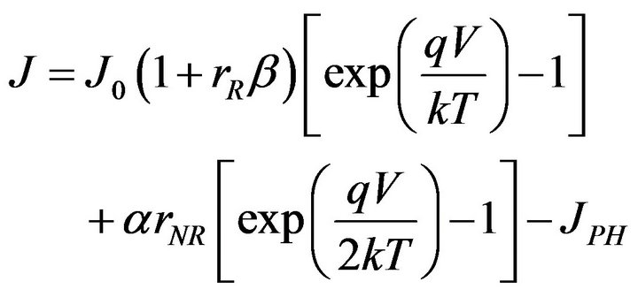
A MQW solar cell with NW wells each of width LW in the intrinsic region of length W with barrier band gap EgB and well band gap EgW was studied in previous works [12]. Under these conditions, the current-voltage relation of the MQW cell is given by:
 (1)
(1)
where q is the electron charge, V is the terminal voltage, kT is the thermal energy, 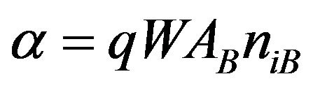 and
and

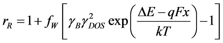
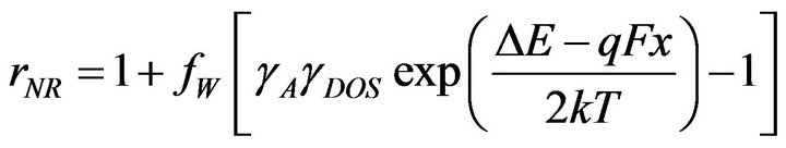
J0 is the reverse saturation current density, AB is the non-radiative coefficient for barriers in the depletion region, which is related to barrier non-radiative lifetime τB by AB = 1/τB, BB is the radiative barrier recombination coefficient, which includes the charge-neutral Shockley injection current, and the space-charge region radiative current, niB is the equilibrium intrinsic carrier concentration for the barrier material, rR and rNR are the radiative enhancement ratio and non-radiative enhancement ratio respectively, and represent the fractional increase in radiative and non-radiative recombination in the intrinsic region, due to the insertion of the quantum wells. These parameters are given by the following expressions:
 (2)
(2)
 (3)
(3)
where DE = EgB – EgW, fW is the fraction of the intrinsic region volume replaced by quantum well material, gDOS = gW/gB is the density of states enhancement factor, with gW and gB as the effective density of states for the wells and barriers, and γB, gA are “oscillator enhancement factor” and “lifetime reduction factor”, respectively. The built in field is denoted by F and x is the position in the wells, so rR and rNR are position dependent. The photocurrent JPH is calculated from the quantum efficiency of the cell. The p-region and n-region contribution to QE was classically evaluated solving the carrier transport equations at room temperature within the minority carrier and depletion approximations. The contribution of photo-generated carriers in the intrinsic region to QE values is calculated by the expression:
 (4)
(4)
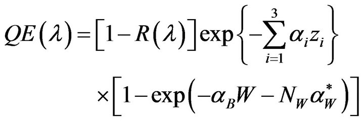
where R(l) is the surface reflectivity spectrum of the antireflection layer. The first exponential factor is due to the attenuation of light in the layers between the surface of the cell and the depletion layer (see Figure 1). The layers considered in our calculus, which are depicted in Figure 1" target="_self"> Figure 1 by numbers, are: 1) antireflection layer; 2) emitter layer; and 3) space-charge region from to the emitter layer. On the other hand, ai and zi are the absorption coefficient and the width of these precedent layers, respectively, the aB is the absorption coefficient of the bulk barrier material, and  is the dimensionless quantum well absorption coefficient, used for energies below the barrier band gap.
When mixing between light and heavy valence subands is neglected, the absorption coefficient can be calculated as follows:
 (5)
(5)
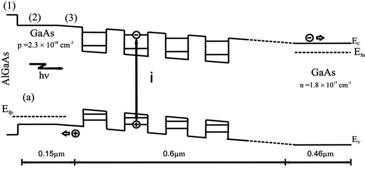
Figure 1. Sketch of energy band diagram of a GaAs p-i-n solar cell with quantum wells inserted within the intrinsic region.
 (6)
(6)
where  and
and  are sums over well states n and m, which numbers depend on the quantum wells width and depth,
  and
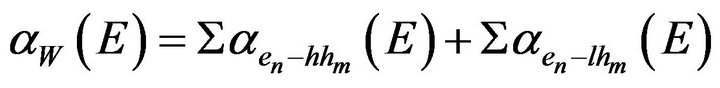
and  are the absorption coefficients due to electron-heavy hole and electron-light hole transitions to conduction band, respectively; αW is the well absorption coefficient and L is the ‘‘quantum thickness of the heterostructure’’. To match accurately with experimental data in the long wavelength region, the exciton absorption is considered in the theoretical calculation. The exciton binding energies are analytically evaluated in the framework of fractional-dimensional space.
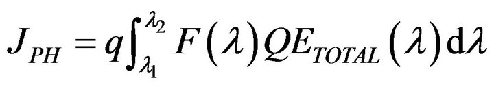
Once the total QE is calculated, by means of the AM1.5 solar spectrum F(l), the photocurrent is determined by integration:
 (7)
(7)
where l1 and l2 are limits of the taken solar spectrum.
Then, Equation (1) is completely determined and conversion efficiency (h) can be evaluated. The present model was previously corroborated comparing experimental quantum efficiency and open circuit voltage with the corresponding calculated values using AlGaAs/GaAs MQWSC sample from the research group at Imperial College London [12].
2.2. Superlattice Solar Cell (SLSC)
In a QWSC, the different quantum wells are independent and there is no coupling between neighboring quantum wells. However, for the superlattice solar cell, there is an interaction between neighboring wells and the wave function becomes extended over the whole superlattice, and the discrete levels in isolated quantum wells spread into a miniband. In presence of electric field across the intrinsic region, perpendicular to the layers, the superlattice minibands split into a band energy ladder and as the electric field is increased, considering wells of equal width with a single energy level; an alignment between the energy subbands is getting worse.
On the other hand, when wells have more than a single quantum energy level, it is expected that the bands move in and out of alignment as the field is varied. This effect reduces tunneling current causing a decrease of the solar cell performance. This way, the electric field causes a localization of the electron in the quantum well that produces vanishing of the miniband, and then the superlattice advantages disappear. Hence, the major challenge is to achieve the conditions for resonant tunneling for a specific value of the electric field which allows the escape of the carrier from the superlattices. This difficulty is overcome fabricating variable spaced superlattice where a well width variation is chosen so that the electron levels are resonant at the operating bias.
From the theoretical point of view, the advantages of an SLSC over an MQWSC are the following: 1) provides quantum levels for electrons and holes within specific eigenenergies (minibands); 2) enhances the miniband absorption; 3) eliminates deep-level recombination between single and double heterojunction; 4) the carriers are capable of tunneling along the growth direction through thin barriers while they are essentially free along the transverse direction; and 5) allows an efficient escape rate of carriers out of quantum wells, which are collected in the emitter and base regions.
In a SLSC, the optical transitions take place between minibands and not between quantum levels, so optical transitions between electron, heavy, and light holes minibands must be included in the J-V characteristic. Equation (1) can be extended to describe a SLSC taking into account that the coefficients (Equations (2) and (3)) and the photocurrent JPH should be related to superlattice structure. Now, the fW factor is the intrinsic region fraction replaced by superlattices, with gSL and gB as the effective density of states for superlattices and barriers, γB = BSL/BB and gA = ASL/AB are the radiative and non radiative recombination coefficients which are referred to superlattices and barriers respectively. The photocurrent is evaluated including the miniband absorption coefficients. We calculated the effective density of states, the absorption coefficient, the radiative recombination coefficient and the photocurrent in a superlattice system in order to determine the J-V characteristic for a SLSC.
The density of states N(E), for a superlattice was estimated considering that each state of energy in a single quantum well becomes the bottom of a two dimensional subband in the density of states. In the same way, each Bloch state in a superlattice behaves as the bottom of a subband. The cosine approximation for a singe miniband of width G was considered. Once N(E) is known, assuming an instantaneous transition at the barrier band edge to the usual three dimensional density of states, considering that the miniband energy extends only the length of the cluster LSL and making the Boltzmann approximation to the Fermi-Dirac distribution, the effective density of states for electrons was found [4]:
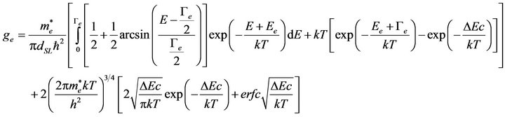 (8)
(8)
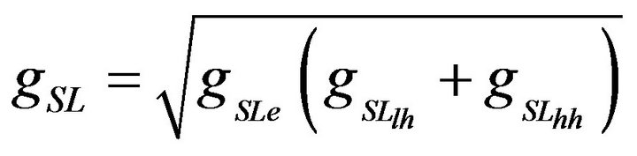
where Ee is the electron miniband bottom, erfc is the complementary error function, me is the electron effective mass, ΔEc = Qc(EgB – EgW) is the conduction band well depth, Qc is the band offset, dSL is the superlattice period and e is the conduction miniband width. Analogous expressions are held for the heavy hole and light hole effective density of states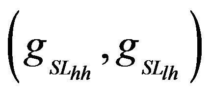 . Then the total superlattice effective density of states was calculated as:
 (9)
(9)
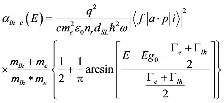
The absorption coefficient for the transitions between light hole and electron minibands was also computed as a function of their widths, Glh and Ge:
 (10)
(10)
where  is the matrix element between the initial i and the final f states, a is a unit vector in the direction of propagation, the momentum p is a differential operator, nr is the heterostructure refraction index, ε0 is the vacuum dielectric constant, ω is the radiation frequency, mlh is the light hole effective mass,
  and Elh is the light hole miniband top. A similar expression of the absorption coefficient is found for the transitions between heavy hole and electron minibands
 . Hence, the superlattice absorption coefficient can be written as:
 (11)
(11)
The absorption allows us to evaluate the radiative recombination loss in Equation (1). According to detailed balance theory, assuming a quasi-Fermi level separation constant and equal to the applied voltage V, the radiative recombination coefficient is given by:
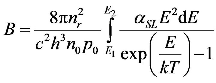 (12)
(12)
The Equation (4) should be modified to consider the absorption of photons through a miniband and not by means of the quantum well discreet levels. The contribution of photo-generated carriers in the intrinsic region to QE values is calculated by the expression:
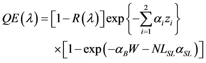 (13)
(13)
where LSL is the superlattice width or cluster width and N is the number of clusters.
Once the expressions for the effective density of states, the absorption coefficient, the radiative recombination coefficient, and photocurrent were found for SLSC, it is possible to evaluate the J-V characteristic (Equation (1)). It is then possible to calculate the conversion efficiency.
3. Results and Discussion
3.1. Strain-Balanced GaAsP/InGaAs/GaAs SB-QWSC
The SB-QWSC is a GaAs p-i-n solar cell with quantum well layers incorporated into the i-region with InGaAs as well material and GaAsP as barrier material. Figure 2 shows the band-structure of the GaAsP/InGaAs/GaAs SB-QWSC modeled in this work.
The compressive strain in the InGaAs QW is matched by tensile strain in GaAsP barriers, overcoming the lattice-mismatch limitation. The GaAsP and InGaAs layer widths were chosen to ensure the average lattice parameter across the i-region was equal to that of GaAs. Elastic constants were considered to evaluate the tensile and compressive strain in GaAsP and InGaAs layers. Thus, if LB is the barrier width, LW is the well width, 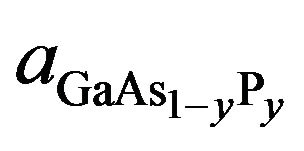 and
and 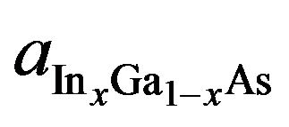 are the respective well and barrier lattice constants; we define:
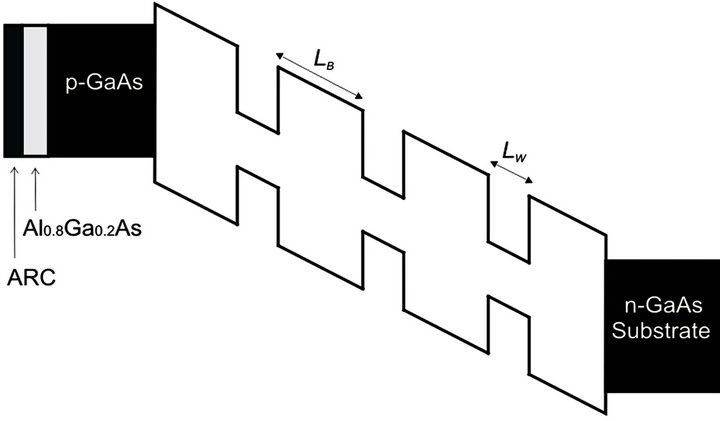
Figure 2. The schematic band-structure of the SB-QWSC. The QW stack is embedded within the depletion zone of the GaAs cell and extends the absorption edge of the cell beyond that of a classical GaAs solar cell.
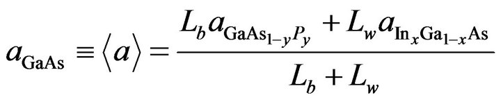 (14)
(14)
The p and n regions were designed with 200 and 500 nm widths respectively, and a 40 nm Al0.8Ga0.2 As window layer was incorporated into the p-region to reduce front surface recombination. The hole and electron concentrations are p = 1018 cm−3 and n = 1018 cm−3, respectively. The ARC is a 70 nm MgF:SiN layer. A passivation layer in the solar cell rear with 200 cm/s surface recombination velocity was assumed.
Biaxial strain can only be achieved on the nanoscale, giving nanostructured solar cells a fundamental advantage over bulk semi-conductor solar cells. The changes of band structure of the layer under strain have significant effects on the SB-QWSC. The growth of strained GaAsP and InGaAs layers allows a wider choice of P and In compositions to fit the energy levels in the quantum wells. Thus, the balanced strain between GaAsP and InGaAs layers is also designed as an extra parameter to tailor the layer materials and the SB-QWSC performance.
The total strain in the layer may be resolved into a hydrostatic component and an axial component. For unstrained bulk material, the heavy hole (hh) and light hole (lh) bands at the top of the valence band are degenerate at the Brillouin zone centre. The hydrostatic component of strain acts on the band edges, thereby changing the band gaps. However, it is the axial strain component, acting on degenerate bands such as in the valence bands. In the valence band, the axial component lifts the degeneracy that exists for the heavy-hole and light-hole bands at the band edge ( point). Under compressive strain, bottom energy of the conduction band is displaced to higher energy and the valence band splits, with the lh band moving further from the conduction band suppressing the lh transition [13]. On the contrary, under tensile strain the GaAsP band gap is reduced and the highest valence band is the light hole band. Consequently, when the In an P compositions are varied, the strains in the barrier and well layers modify absorption threshold in both layers.
The lattice constant of the epitaxial layer in the growth interface is forced to be equal to the lattice constant of the substrate. Therefore, there is an in-plane strain , where i, j = x, y, z. For biaxial strain in (001) plane in the strained layers, the
 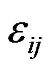 values along [001] direction are
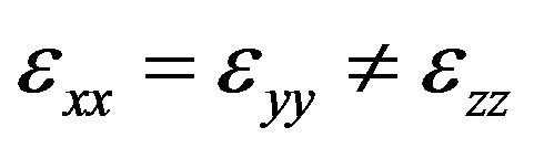 .The strain causes changes of the band edges at the
  point, which are given by:
 (15.1)
 (15.2)
 (15.3)
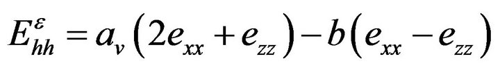
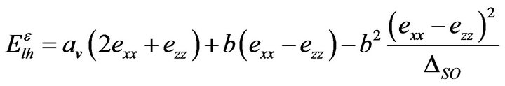
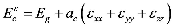
where ,
,  and
and  are the new energy level values under strain for heavy and light holes and electrons, respectively, Eg is the band gap, an and ac are so-called hydrostatic deformation potentials, b is the shear deformation potential and DSO is the spin-orbit splitting of the VB at G point. The separation of the total hydrostatic deformation potential in conduction (ac) and valence band (an) contributions is important at heterointerfaces.
Varying the wave vector  values, the E versus k diagram is obtained for both materials, InGaAs and GaAsP, which are shown in Figure 3. Note that due to
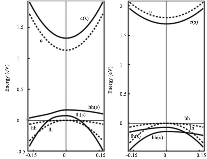


Figure 3. Representation of the effect of strain on bandedges around of the first Brillouin zone center. In unstrained bulk material the valence band is degenerate at the zone centre (dashed line). c(s) is the strain conduction bands, lh(s) and hh(s) are the strain light and heavy hole bands, respectively (straight line). The vertical axes give the energy in eV, the lateral axes give the wave number kx and kz, respectively; (a) Shift and deformation of In0.2Ga0.8As energy bands for compressive strain, exx = −0.014; ezz = 0.013; (b) Of GaAs0.7P0.3 energy bands for tensile strain exx =0.019; ezz= −0.010.
strains, the In0.2Ga0.8 As layer experiences a 121 meV band gap increment, while for GaAs0.7P0.3 layer a decrease of 176 meV is obtained. When the In and P compositions as well as their layer widths are varied, such that the condition given by Equation (14) is satisfied, the strain is changed in the well and barrier layers, causing in both films a deviation in the absorption threshold.
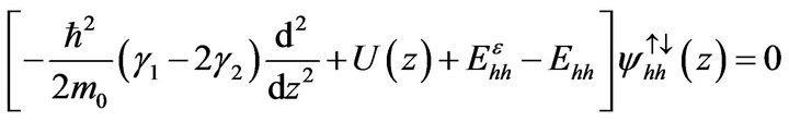
The envelope function approximation is here assumed to compute QW energy levels in conduction band. The electron energy Ee and wave function ye can be calculated with the effective mass approximation. Then, the motion of the conduction band electron in the QW is described by Schrödinger equation. In order to determine the QW energy levels in the hh and lh bands under varying compressive strain a 4 × 4 k∙p Kohn-Luttinger Hamiltonian  was used:
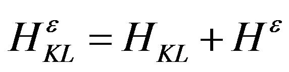 (16)
(16)
where HKL is the Kohn-Luttinger Hamiltonian without strain and H is the strain Hamiltonian that for epilayers grown in [001] direction is given by:
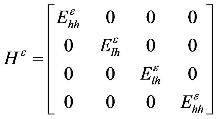 (17)
(17)
In a QW system, some splitting of the confined valence band levels takes place due to the differences in effective mass. This splitting can be greatly enhanced if the QW is strained. When the well material is strained we have the confinement effects, but in addition we have the consequences of the non-degenerate bulk band edges. For example under (001) biaxial compressive strain the lh band is shifted further energetically from the conduction band. In a sense, compressive strain acts in the same manner as the effect of confinement.
Then, biaxial strain, in well and barriers layers, lifts the degeneracy in the valence band such that it is possible to considerer independently the hh and lh bands. Under above approximations, the QW energy levels for hh and lh bands were found.
Schrödinger equation corresponding to  Hamiltonian is not separated so it is assumed that the “off-diagonal” terms, which lead to valence band mixing, are small enough that they can be neglected. With this assumption the Schrödinger equation becomes separable:
 (18)
(18)
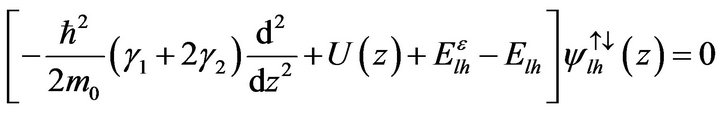 (19)
(19)
where  and
and  are the envelope functions with spin direction. The Equations (18) and (19) are solved in barrier and well regions with the corresponding
  potential and Konh-Luttinger parameter (
 and
and ) values in each layer. Computed the Ee, Eh and Elh values the optical transitions are calculated by Fermi’s golden rule and the Equation (6) is evaluated to determine the absorption in the quantum wells. Then, the procedure to calculate the photocurrent is analogous to that described in 2.1.
The QE as a function of wavelength was computed by means of Equation (4) and compared with qt1897b sample from Quantum Photovoltaic Group at Imperial College of London. The cell is a p-i-n diode with an i-region containing five QWs that are 9.6 nm wide of compressively strained In0.16Ga0.84 As inserted into tensilestrained GaAs0.91P0.09 barriers at strain-balance condition.
Figure 4 displays typical example of good agreement to quantum efficiency between experimental data and the theoretical calculations without any fitting parameter. The QWs extend absorption from GaAs bulk band-gap  to threshold energy determined by the confinement energy. The extra absorption is shown in the inset of Figure 4, at wavelengths in excess of the GaAs band gap, the cell absorption is extended to 980 nm, leading an increment in the short circuit current. The GaAsP barriers are responsible for the small drop in quantum efficiency at their absorption edge (835 nm). Similarly, it is possible to note the strain effect: the absorption is reduced in the long wavelength range with strain because the energy difference between Ee and Eh or Elh quantum well levels is smaller.
The strain and electric field effects that do not explicitly

Figure 4. Modelled and experimental quantum efficiency versus wavelength for 5 wells qt1897b sample from the Quantum Photovoltaics Group of Imperial College. The inset shows the wavelength range dominated by the QW absorption with and without strain. A good agreement with the experimental data is achieved. The e1-hh1 exciton peak is seen to shift to lower wavelengths with the strain effect.
show in Equation (1) were considered to evaluate the J-V characteristic. When the In and P compositions are varied or their width layer are changed, the generated strain modifies the absorption threshold. In a QW system, some splitting of the confined valence band levels takes place due to the differences in effective mass. This splitting can be greatly enhanced if the QW is strained. Similarly, when W is changed, the electric field variation also modifies the absorption threshold.
The dependence of conversion efficiency on In and P composition is examined in Figure 5 for LW = 15 nm. In and P composition are varied in the range from 0.5% to 20% during the development process of the contour plot.
The LB values are varied in order to satisfy strain-balanced condition (Equation (14)). The white region corresponds to In and P compositions for which the optical transitions between the ground heavy hole and electron QW levels are larger than GaAs bandgap. These optical transitions were not considered in the calculations. Figure 6 shows that the In fraction influences more in the conversion efficiency than P fraction. Enlarging In composition in the QW, the layer barrier width must be increased to settle down strain-balanced condition, leading to larger radiative and no-radiative recombination in the barrier region that increases the leakage current. Otherwise, with P fraction variation, the recombination process does not significantly change, in comparison with In case, due to a slightly reduction of the barrier width. Besides this behavior, the P fraction increment originates enhancing of absorption threshold in the strained barrier that reduces the absorbed photon number of the solar spectrum such that the photocurrent decreases slightly. We can conclude that the In composition is the critical factor in the SB-QWSC performance. Additionally, note from Figure 6, that until 3% In and 5% P compositions, a conversion efficiency so high as 27 % is reached.
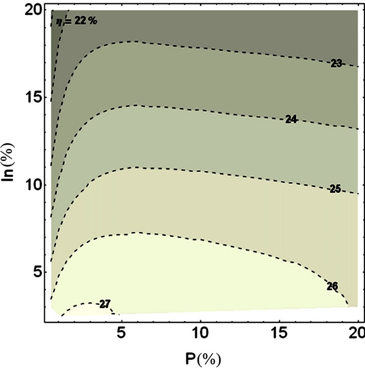
Figure 5. Contour plot for conversion efficiency versus In and P compositions for Lw = 15 nm, and Nw = 20. It shows that the In fraction influences more in the conversion efficiency than P fraction.
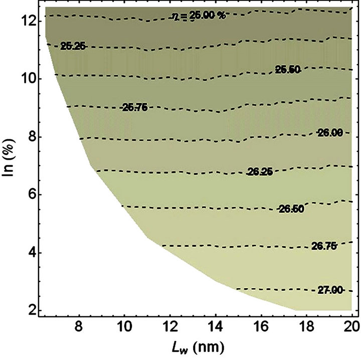
Figure 6. Contour plot for conversion efficiency as a function of In composition and quantum well width for P composition, y = 0.04. Intrinsic region of length ~1 mm was taken. High efficiencies are reached in a wide range of In composition and quantum well width values.
The dependence of conversion efficiency on In composition and quantum well width is shown in Figure 6 for a 4% of P composition. Intrinsic region of length ~1 mm was taken where it begins and finishes with barrier layer. In composition and LW are varied in the range from 0.5% to 20% and 4 nm to 20 nm, respectively, during the development process of the contour plot. In this case, LB and NW were necessarily varied to satisfy strain-balanced condition. The broken lines are due to the emergence of QW energy levels when the well width and barrier height are increased.
For an In composition given, as it can be observed in Figure 6, the conversion efficiency is almost insensitive to  because there is a compensation effect. Increasing the quantum well width the photon absorption is enlarged but the barrier layer is also increased and the well number in a fixed W is reduced and consequently the absorption photons decreases. High efficiencies are reached in a wide range of In composition and quantum well width values with a maximum at x = 0.02 and LW = 18 nm.
3.2. GaAs/GaInNAs MQWSC and SLSC
A GaAs p-i-n solar cell is modeled where the i-region is filled with GaAs/GaInNAs multiple quantum wells. The electron and hole concentrations, in base and emitter regions are 1.8 × 1017 cm−3 and 2.3 × 1018 cm−3, respectively, while their widths are 0.15 mm (p-region), 0.60 mm (i-region), and 0.46 mm (n-region). A 40 nm Al0.8Ga0.2As window layer was incorporated into the p-region to reduce front surface recombination and a 70 nm MgF:SiN layer as ARC was used.
In order to investigate the GaAs/Ga1-xInxNyAs1-y MQWSC conversion efficiency, small nitrogen concentrations were considered to modify the quantum well depth. Also, the x = 2.85y condition was satisfied so that Ga1-xInxNyAs1-y lattice matches to GaAs. GaInNAs parameters were taken from reference [14]. High values of conversion efficiency are reached up to 3% N composition [15], as depicted in Figure 7. The maximum values of efficiency are obtained for a narrow region around 1% of nitrogen composition and narrow quantum well widths. These N compositions correspond to shallow quantum wells, where the carrier generation overcomes the recombination. Also, for these N fractions a second quantum level appears in the heavy hole band slightly increasing photon absorption. When the quantum wells are deeper (nitrogen percent increases) the carrier recombination is increased and the conversion efficiency falls. Figure 7 also shows the conversion efficiency dependence on quantum well width. For 1% nitrogen composition, h is practically insensitive to quantum well width because there is a compensation effect. This result could be explained because there is a trade-off between quantum well width and quantum well number, for wider quantum wells the photons absorption is greater, but the quantum well number inserted in the constant intrinsic region (0.6 mm) is smaller. On the other hand, narrow quantum wells absorb less photon but it is possible to insert more of them in the intrinsic region, then the absorption overcomes the recombination at the 1% N concentration. For any nitrogen compositions higher than 1%, the efficiency falls when the quantum well width increases since the carrier recombination is increased.
GaAs/GaInNAs solar cells were studied inserting now superlattices in the i-region of a GaAs p-i-n solar cell, keeping the other device parameters identical.
The conditions for resonant tunneling were computed by the well-known transfer matrix method (TMM) without back-scattered wave. A variably spaced multiple quantum well or superlattice was considered to enhance the resonant tunneling between adjacent wells [11]. The
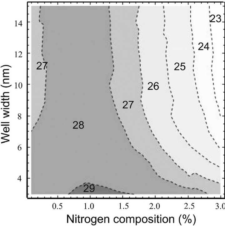
Figure 7. Contour plot of GaAs/GaInNAs MQWSC efficiency as a function of the quantum well width and the nitrogen.
resonance takes place at 12 kV/cm, which was evaluated taking into account the uniform doping levels, p and n-regions, and intrinsic region width. We have used a fixed field (a parameter in our model), which is not such a difficult thing to do experimentally, once that doping levels and intrinsic thickness are as those reported here.
To study the GaAs/GaInNAs SLSC performance, some different arrangements with ten variably spaced multiple quantum wells (clusters) were optimized to enhance the resonant tunneling between adjacent wells. These clusters are composed by quantum wells of 1% nitrogen composition and barriers of 1 nm wide. A series of clusters are inserted in the i-region, independent from each other, in such a way that there is no coupling between neighboring clusters.
Figure 8 shows a contour plot of the conversion efficiency for the SLSC as a function of the width and the number of clusters. The first thing to highlight is that the SLSC conversion efficiencies are as much as 3% higher than those of the MQWSC. The AB contour in Figure 8 corresponds to the pair of values (cluster number and cluster width) where the highest conversion efficiency is reached. It can be also observed that while the width and the number of cluster increase, the conversion efficiency is increased because the photon absorption is higher. For this reason, it is suitable to add smaller clusters length in the intrinsic region, keeping wide wells, to enhance the conversion efficiency. It could be though that it is possible to increase the conversion efficiency by adding more clusters in the intrinsic region but it is not true at all because when more clusters are inserted the recombination process is increased, being necessary to get a balance between generation and recombination. Besides, with the incorporation of more clusters in the intrinsic region, the absorption processes increase, moving forward less photon to the deepest layers in the device, originating a decrease of the photogenerated carriers. For this reason,

Figure 8. Contour plot of GaAs/GaInNAs SLSC efficiency as a function of the cluster width and number.
the indefinite incorporation of clusters does not mean that the photocurrent also increases, but spreading to saturation as long as the open-circuit voltage falls due to the increment of the recombination.
4. Conclusions
A model for quantum well and superlattice solar cells was developed and used to theoretically study broad qualitative tendencies in quantum solar cell performance. Results from this research provide a more comprehensive picture of these devices and should supply a profitable guide for its designing. The model allows optimizing the solar cell performance as a function of several solar cell parameters. The well and barrier band gaps, the width and depth of the wells, the number of the wells in the intrinsic region are considered in the model to achieve the maximum conversion efficiency.
A GaAsP/InGaAs/GaAs strain-balanced solar cell was optimized to reach the maximum performance. The electric field and stress, tensile and compressive, were considered. Our model was used to determine the highest efficiencies for cells containing quantum wells under varying degrees of strain. The strain-balanced multiple quantum well solar cells show a high conversion efficiency that it makes very attractive for space applications or for a triple-junction concentrator cell based on a GaAsP/InGaAs /GaAs middle cell. Solar cells containing strain balanced QWs in a multi-junction solar cell allow the absorption edge of each subcell to be independently adjusted. QWs provide an alternative means for tailoring the current generated or  in a solar cell.
We have shown a new type of photovoltaic device where GaAs/GaInNAs multiple quantum wells or superlattice are inserted in the i-region of a GaAs p-i-n solar cell. A theoretical model was developed to study the performances of these devices. A study of conversion efficiency as function of nitrogen composition and quantum well width was presented which allowed determining the range of these parameters where high conversion efficiencies in MQWSC are reached.
Our results show that conversion efficiencies can be reached which have never been obtained before for a single junction solar cell. Because of the results that our model predictions are neither compared nor confirmed experimentally, it would be interesting to see if future experiments will corroborate our outcomes. Solar cell efficiency potential remains far greater than solar cell efficiencies, including those achieved in research laboratories. New approaches are necessary in order to increase the conversion efficiency and the GaAs/GaInNAs solar cells could be a road to reach this goal. The GaAs/ GaInNAs MQWSC or SLSC show high conversion efficiency. They make very attractive for space applications or for a triple-junction concentrator cell based on a GaAs/GaInNAs bottom cell that could reach 50% conversion efficiency.
5. Acknowledgements
Thanks to COZCYT for the partial financial support for this paper.
REFERENCES
- K. W. J. Barnham and C. Duggan, “A New Approach to High-Efficiency Multi-Bandgap Solar Cells,” Journal of Applied Physics, Vol. 67, No. 7, 1990, pp. 3490-3493. doi:10.1063/1.345339
- J. Nelson, M. Paxman, K. W. J. Barnham, J. S. Roberts and C. Button, “Steady-State Carrier Escape from Single Quantum Wells,” IEEE Journal of Quantum Electronics, Vol. 29, No. 6, 1993, pp. 1460-1465. doi:10.1109/3.234396
- M. Paxman, J. Nelson, K. W. J. Barnham, B. Braun, J. P. Connolly, C. Button, J. S. Roberts and C. T. Foxon, “Modeling the Spectral Response of the Quantum Well Solar Cell,” Journal of Applied Physics, Vol. 74, No. 1, 1993, pp. 614-621. doi:10.1063/1.355275
- M. Courel, J. C. Rimada and L. Hernández, “AlGaAs/ GaAs Superlattice Solar Cells,” Progress in Photovoltaics: Research and Applications, Vol. 21, No. 3, 2012, pp. 276-282. doi:10.1002/pip.1178
- P. R. Griffin, J. Barnes, K. W. J. Barnham, G. Haarpaintner, M. Mazzer, C. Zanotti-Fregonara, E. Grunbaum, C. Olson, C. Rohr, J. P. R. David, J. S. Roberts, R. Gray and M. A. Pate, “Effect of Strain Relaxation on Forward Bias Dark Currents in GaAs/InGaAs Multiquantum Well p-i-n Diodes,” Journal of Applied Physics, Vol. 80, No. 10, 1996, pp. 5815-5820. doi:10.1063/1.363574
- N. J. Ekins-Daukes, K. W. J. Barnham, J. P. Connolly, J. S. Roberts, J. C. Clark, G. Hill and M. Mazzer, “StrainBalanced GaAsP/InGaAs Quantum Well Solar Cells,” Applied Physics Letters, Vol. 75, No. 26, 1999, pp. 495- 497. doi:10.1063/1.125580
- D. C. Johnson, I. Ballard, K. W. J. Barnham, M. Mazzer, T. N. D. Tibbits, J. Roberts, G. Hill and C. Calder, “Optimisation of Photon Recycling Effects in Strain-Balanced Quantum Well Solar Cells,” Proceedings of the 4th World Conference on Photovoltaic Energy Conversion, Hawaii, 7-12 May 2006, pp. 26-31.
- M. Kondow, K. Uomi, A. Niwa, T. Kitatani, S. Watahiki and Y. Yazawa, “GaInNAs: A Novel Material for LongWavelength-Range Laser Diodes with Excellent HighTemperature Performance,” Japanese Journal of Applied Physics, Vol. 35, Pt. 1, 1996, pp. 1273-1275. doi:10.1143/JJAP.35.1273
- D. J. Friedman and S. R. Kurtz, “Breakeven Criteria for the GaInNAs Junction in GaInP/GaAs/GaInNAs/Ge FourJunction Solar Cells,” Progress in Photovoltaics, Vol. 10, No. 5, 2002, pp. 331-344. doi:10.1002/pip.430
- A. Freundlich, A. Fotkatzikis, L. Bhusal, L. Williams, A. Alemu, W. Zhu, J. A. H. Coaquira, A. Feltrin and G. Radhakrishnan, “III-V Dilute Nitride-Based Multi-Quantum Well Solar Cell,” Journal of Crystal Growth, Vol. 301- 302, 2007, pp. 993-996. doi:10.1016/j.jcrysgro.2006.11.256
- E. Reyes-Gómez, L. E. Oliveira and M. de Dios-Leyva, “Quasi-Bond States and Intra-Band Transition Energies in GaAs-(Ga,Al)As Variably Spaced Semiconductor Superlattices,” Physica B, Vol. 358, No 1-4, 2005, pp. 269-278. doi:10.1016/j.physb.2005.01.462
- J. C. Rimada, L. Hernández, J. P. Connolly and K. W. J. Barnham, “Conversion Efficiency Enhancement of AlGaAs Quantum Well Solar Cells,” Microelectronics Journal, Vol. 38, No. 4-5, 2007, pp. 513-518. doi:10.1016/j.mejo.2007.03.007
- K. W. J. Barnham and D. Vvedensky, “Low-Dimensional Semiconductor Structures,” Cambridge University Press, Cambridge, 2001, pp. 280-286. doi:10.1017/CBO9780511624247
- S.-H. Yen, M.-L. Chen and Y.-K. Kuo, “Gain and Threshold Properties of InGaAsN/GaAsN Material System for 1. 3-μm Semiconductor Lasers,” Optics & Laser Technology, Vol. 39, No. 7, 2007, pp. 1432-1436. doi:10.1016/j.optlastec.2006.10.003
- M. Courel, J. C. Rimada and L. Hernández, “GaAsGaInNAs Quantum Well and Superlattice Solar Cell,” Applied Physics Letters, Vol. 100, No. 7, 2012, pp. 073508-11. doi:10.1063/1.3687195