Advances in Materials Physics and Chemistry
Vol.06 No.08(2016), Article ID:69456,9 pages
10.4236/ampc.2016.68024
Characteristics Improvement of PEDOT:PSS Transparent Conductive Film Prepared by Ink-Jet Printing
Atsushi Nitta1*, Kazuya Kawahara2, Kohei Miyata2
1Department of Electronic Control Engineering, National Institute of Technology, Kagoshima College, Kirishima, Japan
2Advanced Mechanical and Electronic Systems Engineering, National Institute of Technology, Kagoshima College, Kirishima, Japan

Copyright © 2016 by authors and Scientific Research Publishing Inc.
This work is licensed under the Creative Commons Attribution International License (CC BY).
http://creativecommons.org/licenses/by/4.0/


Received 30 June 2016; accepted 30 July 2016; published 4 August 2016
ABSTRACT
Recently, a high-performance and low-priced transparent conductive film has been expected to be developed because flexible devices produced using organic materials have been actively studied. An indium tin oxide (ITO) thin film, which has been generally used as a material for a transparent conductive film, has problems, such as fragility to bending stress and depletion of the resource. The present study used poly(3, 4-ethylenedioxythiophene)/poly(styrenesulfonate) (PEDOT:PSS), an organic electroconductive material, and examined the improvement in the resistance value and visible light transmittance of a transparent conductive film produced using the ink-jet method. In previous studies, we reported that, to improve the resistance value and visible light transmittance of a thin film, it was effective to clean the film substrate with ultraviolet/ozone (UV/O3) treatment, anneal the film after it was deposited on the substance, and dip the annealed film into a polar solvent. Focusing on the thin film processing between printing operations, the present study improved resistance value and visible light transmittance by examining both the application methods of a polar solvent and the annealing time between printing operations. As a result, the resistance value and visible light transmittance of a PEDOT:PSS thin film were 390.4 Ω and 86.6%, respectively. This film was obtained by applying a polar solvent and performing annealing for 30 min between printing operations. The printing was performed three times.
Keywords:
PEDOT:PSS, Ink-Jet Printing, Transparent Conductive Film, Flexible Devices

1. Introduction
Recently, studies on flexible devices produced using organic materials and carbon nanotubes (CNTs) have been briskly conducted [1] - [4] . Ohno et al. of Nagoya University in Japan and a research team of Aalto University in Finland developed an all-carbon integrated circuit composed of transistors and wires, which were made of only CNTs, for the first time in the world due to the optimization of CNT thin film-forming technologies [5] . Devices such as electroluminescence displays, thin-film solar cells, and transistors produced using organic materials have been positively developed [6] - [11] . In these electronic devices, transparent electrodes, which transmit visible light and possess conductivity, are important components. At present, an ITO thin film is the most frequently used as a material for a transparent conductive film [12] - [15] . However, because an ITO thin film contains indium, rare metal, depletion and price rise of the resource have been at issue. Moreover, because an ITO thin film shows fragility to bending stress, this film is not suitable for flexible devices. To solve these problems, various materials such as organic materials, metallic nanoparticles, CNTs, and oxide-based materials have been studied [16] - [21] . In particular, organic materials are noteworthy because a film can be formed using low-temperature processes, such as printing and coating. As a result, cheap devices can be manufactured [22] [23] .
At present, printed electronics technology, which is a device manufacturing method using printing technologies, has been actively studied [24] - [26] . As the study of printed electronics advances, certain types of electronics equip- ment are expected to be produced using only this method [27] . By using printing technologies for device manufacturing, the number of processes, initial investment in manufacturing facilities, electric energy consumption, and material consumption can be largely reduced, compared to a conventional method of combining vacuum film formation with photolithography. However, to use printing technologies, a material must be prepared in the form of ink, the prepared ink must be optimized, and the surface of a film must be even during printing.
If a practicable transparent conductive film can be produced using a simple and cheap method, such as a printing method, not only electrodes but also electronic apparatuses can be manufactured at low cost. However, the performance of an organic, transparent conductive film must be improved. If so, the film cannot be practically used.
We have paid attention to PEDOT:PSS, an organic electroconductive material exhibiting high flexibility and conductivity, as a substitute for ITO. We have aimed to produce a cheap and flexible transparent conductive film by forming the film on a plastic film substrate using an ink-jet printer. In previous studies, we improved the characteristics of a PEDOT:PSS thin film based on its resistance value and visible light transmittance and revealed that cleaning the plastic film substrate with UV/O3, annealing the film after it was deposited on the substrate and dipping the film into a polar solvent was useful [28] . In the present study, we examined the effects of both the application of a polar solvent on the film each time after a layer was printed, and the annealing time between printing operations on the improved characteristics of a PEDOT:PSS thin film.
2. Experimental
Preparation and Evaluation of a Thin Film
In the present study, CLEVIOS (CleviosTM PH500) was used as PEDOT:PSS. CLEVIOS PH 500 possesses excellent conductivity, permeability, and flexibility. Since the mechanical flexibility of CLEVIOS PH 500 is high, it can be used for various printing methods, including spin coating and dip coating. Figure 1 shows the molecular structure of PEDOT:PSS, and Table 1 shows its physical properties. To reduce the viscosity and surface tension of ink, ethanol―a low-boiling point solvent―and ethylene glycol―a high-boiling point solvent which is reported to remove insulative PSS and form a conductive region consisting of conductive PEDOT―were used as additives [29] . Similar to a previous report, we adopted the ink composition of PEDOT:PSS:ethanol:ethylene glycol = 70:20:10 wt% [28] .
To produce a PEDOT:PSS thin film, a piezo-type, pigment-based, ink-jet printer (PX-105; Seiko Epson CO.) was used. For the printing pattern, 40 mm (length) × 15 mm (width) was adopted. A heat-resistant, transparent film possessing excellent transparency, heat resistance, and chemical resistance (Teonex Q65-FA; Teijin DuPont Films Co., Ltd.) was used as the film substrate. The surface of the film substrate was cleaned using a UV/O3 cleaning and modifying apparatus (ASM401N; Asumi Giken, Ltd.). For the conditions of UV/O3 cleaning, the UV radiation distance was 30 mm, the output of a low-pressure mercury lamp was 40 W, and the cleaning time was 20 min. To evaporate the additives, which remained in the film as impurities after it was formed and adversely affected the resistance value, the thin film was annealed in the drying process. For drying, a constant-temperature

Figure 1. The molecular structure of the PEDOT:PSS.

Table 1. Material properties of the PEDOT:PSS.
drying oven (EOP-300B; As One Co., Ltd.) was used, and the temperature was set at 100˚C, at which the lowest resistance value was obtained in our previous study [28] .
Ethylene glycol was used as a polar solvent. Drying a PEDOT:PSS thin film again after dipping it into a polar solvent was reported to facilitate the arrangement of PEDOT molecules, resulting in the conductivity improvement of the PEDOT:PSS thin film [30] . Our previous study reported that the dipping treatment improved the characteristics of a PEDOT:PSS thin film based on its resistance value and transmittance. In the present study, the polar solvent was splayed on a PEDOT:PSS thin film after each printing, and further improved characteristics were examined. We used a digital multimeter (VOAC7521H; Iwatsu Electric Co., Ltd.) to evaluate the conductivity of the film, a spectrophotometer (U-3900; Hitachi High-Technologies Co.) to evaluate transparency, and a microscope (VHX-1000; Keyence Co., Ltd.) to observe its surface.
3. Results and Discussion
3.1. Examination of Resistance Value and Transmittance According to the Number of Printing Times
In producing a transparent conductive film using the ink-jet method, the resistance value of the film is extremely high when the printing is not performed several times. In the present study, the printing was performed several times in order to reduce the resistance value of the film. Annealing between printing operations was set at 100˚C for 15 min. Annealing was also performed at 100˚C for 60 min after the entire printing process was completed.
Figure 2 shows the changes in the resistance value and visible light transmittance according to the number of printing times. Transmittance was measured at the wavelength of 550 nm. The resistance value of the thin film decreased as the number of printing times increased. The reason for this is probably that the printing patterns became dense and the contact area between PEDOT:PSS particles increased; consequently, the conductivity improved. However, the visible light transmittance decreased as the number of printing times increased. The reason for this is probably that, because PEDOT:PSS is a dark blue liquid, the color of the thin film became darker as the number of printing times increased, resulting in a decrease in visible light transmittance. When the number of printing times was one, since the amount of PEDOT:PSS in the thin film was small, the resistance value was extremely high, and the measured values varied widely. When the number of printing times exceeded five, the visible light transmittance was below 80%, which is characteristic of a transparent conductive film. The present study dealt with thin films printed two to four times while considering the resistance value and visible light transmittance.
3.2. Examination of Treatment Methods Using the Polar Solvent
In our previous studies, the characteristics of a PEDOT:PSS thin film were improved by dipping the film into a polar solvent and drying it. Namely, after the entire printing process was completed, a PEDOT:PSS thin film was dipped into a polar solvent, and the film was annealed at 100˚C for 60 min. In the present study, the characteristics of a PEDOT:PSS thin film were attempted to be improved by spraying a polar solvent on a PEDOT:PSS thin film between printing operations. The annealing between printing operations was set at 100˚C for 15 min. There is a possibility that, when a polar solvent is applied to a PEDOT:PSS thin film after each printing, the arrangement of PEDOT molecules in each layer is facilitated, the aggregates of PEDOT:PSS particles in the entire film are fractionated further, and the conductivity improves.
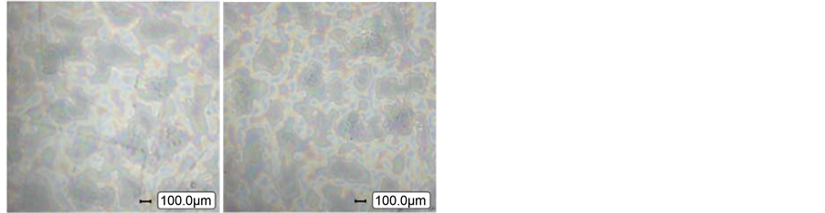
Figure 3 shows images of the surfaces of PEDOT:PSS thin films when the treatment method was changed. In this figure, (a) shows the film surface obtained without using the polar solvent. In the ink-jet method, the aggregation of PEDOT:PSS particles is observed, which was not reported to be observed in film formation methods such as spin coating. It is considered that, in the aggregation of PEDOT:PSS particles, PEDOT molecules are unevenly distributed; consequently, the formation of a conductive region is hindered. Also, in this figure, (b) shows the film surface obtained by performing the dipping treatment in which the unevenly generated aggregates of PEDOT:PSS particles were fractionated and distributed, and (c) shows the film surface obtained by applying the polar solvent to each layer. As shown in (c), the finer aggregates of PEDOT:PSS particles were distributed.
Figure 4 shows the changes in the resistance value according to the number of printing times when the treatment method was changed. The resistance value of the film was lower when applying the polar solvent to each layer than when using the dipping treatment. Therefore, it was revealed that the change in the aggregation state of PEDOT:PSS particles affected the conductivity.

Figure 2. Changes in the resistance value and visible light transmittance according to the number of printing times.
 (a) (b) (c)
Figure 3. Microscope image of the surface of a PEDOT:PSS (annealing temperature: 100˚C, 3 times printing, ×100). (a): No treatment. (b): Dipping treatment. (c): Spraying treatment in each layer.
Figure 5 shows the changes in the visible light transmittance according to the number of printing times when the treatment method using the polar solvent was changed. When the number of printing times was two, since the amount of PEDOT:PSS in the thin film was small, the visible light transmittance varied. However, when the number of printing times was three or four, the visible light transmittance of the film was lower when using the dipping treatment than when not using the polar solvent. The reason for this was probably that the aggregates of PEDOT:PSS particles were fractionated and a homogeneous thin film with a small number of gaps was formed; consequently, the transmission of light was hindered. The visible light transmittance was higher in a thin film obtained by applying the polar solvent to each layer than in a thin film obtained by performing the dipping treat- ment. The reason for this was probably that the aggregates of PEDOT:PSS particles were fractionated, the unevenness on the film surface was reduced, and the scattering of light was inhibited; consequently, the visible light transmittance increased.
Both the conductivity and visible light transmittance were higher in a thin film obtained by applying the polar solvent to each layer than in a thin film obtained by performing the dipping treatment. The surface homogeneity and electrical and optical properties of the thin film were improved by the application method. However, the visible light transmittance was more affected by the number of printing times than by the fractionation of the aggregates of PEDOT:PSS particles. Therefore, by adopting three printing times instead of four, the characteristics of a PEDOT:PSS thin film would improve, and the visible light transmittance would be near 80%.
3.3. Examination of Annealing Time between Printing Operations
Annealing is required each time after printing. Although annealing decreases the visible light transmittance, it can also remove impurities that decrease conductivity from a film. Therefore, when the resistance value is taken into consideration, annealing is indispensable. In the present study, the annealing temperature was set at 100˚C, by which the best characteristics were observed in our previous experiments.
Figure 6 shows images of the surfaces of PEDOT:PSS thin films obtained by changing the annealing time. No change was observed in the surface state of a film due to the annealing time. The surface state of the thin film became more heterogeneous as the annealing temperature increased [28] . In the annealing process, PEDOT:PSS particles can move and aggregate, resulting in an uneven surface. Even though the annealing time was changed, the aggregate state did not change.
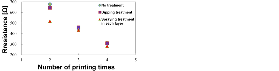
Figure 4. Dependence of the resistance value due to each treatment and the number of printing times.

Figure 5. Dependence of the visible light transmittance due to each treatment and the number of printing time.
Figure 7 shows the changes in the resistance value and visible light transmittance due to the annealing time between printing operations when three printing times were adopted. As shown in this figure, the resistance value decreased with time, and it was lowest when the annealing time was 30 min. After 30 min, the resistance value did not change. Therefore, to remove impurities by annealing, a 30 min annealing time was sufficient. Moreover, no change was observed in the visible light transmittance due to the annealing time. Therefore, when the surface state of a film did not change, the visible light transmittance also did not change.
Next, a thin film was formed by applying the polar solvent to each layer and changing the annealing time between printing operations from 15 to 30 min. Figure 8 shows the changes in the resistance value due to the annealing time and number of printing times. The resistance value decreased when the number of printing times was three or four, and the characteristics of a thin film became stable after formation. In particular, when the number of printing times was three, the resistance value decreased the most. Figure 9 shows the changes in visible light
 (a) (b)
Figure 6. Microscope image of the surface of a PEDOT:PSS (annealing temperature: 100˚C, 3 times printing, ×100). (a): 15 minutes. (b): 30 minutes.
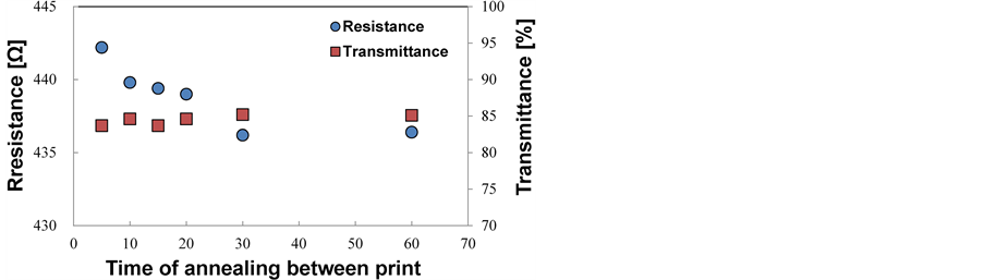
Figure 7. Dependence of the resistance value and visible light transmittance due to the annealing time between printing operations (3 times printing).

Figure 8. Dependence of the resistance value due to the annealing time and the number of printing times.
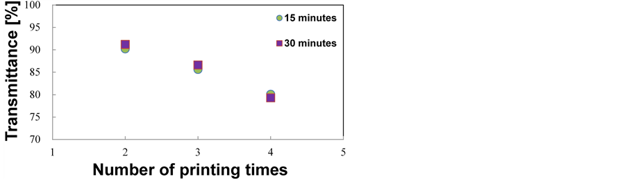
Figure 9. Dependence of the visible light transmittance due to the annealing time and the number of printing times.
transmittance due to the annealing time and number of printing times. The transmittance did not change, although the annealing time was changed. In printing three times, resistance value was 390.4 Ω and the visible light transmittance was 86.6%. As for these values, the resistivity of PEDOT:PSS thin film was nearly twice as high as that of ITO thin film used commonly and visible light transmittance of the former was nearly 3% lower than that of the latter. The lowest resistance value was measured when the number of printing times was four but the visible light transmittance was nearly 80%. The transmittance was more affected by the number of printing times than by the annealing time. When the transmittance is taken into consideration, to reduce the resistance value of a PEDOT:PSS thin film, treatment methods should be examined when the film is formed by three printing times.
4. Conclusions
To improve the characteristics of a PEDOT:PSS transparent conductive film produced using an ink-jet printer, the present study examined not only a method in which a polar solvent was applied to each layer but also the effects of the annealing time between printing operations on the resistance value and visible light transmittance of the produced thin film. Because of the effect of the number of printing times on the resistance value and visible light transmittance, we focused on PEDOT:PSS thin films, which were formed by two to four printing times.
The resistance value was lowered from 459.8 Ω to 434.0 Ω in a thin film obtained by applying the polar solvent to each layer than in a thin film obtained by performing the dipping treatment. The change in the aggregation state of PEDOT:PSS particles was revealed to affect the conductivity. The visible light transmittance was raised 3% or so in a thin film obtained by applying the polar solvent to each layer than in a thin film obtained by performing the dipping treatment. The reason for this was probably that the aggregates of PEDOT:PSS particles were fractionated, the unevenness on the film surface was reduced, and the scattering of light was inhibited; con- sequently, the visible light transmittance increased.
The annealing time between printing operations was examined, and the resistance value was revealed to decrease by performing annealing for 30 min between printing operations. The reason for this is probably that, since impurities in each layer were removed, a conductive region was formed. No change was observed in the surface state of a thin film due to the annealing time, and the annealing time did not affect the transmittance. When drying a thin film for 15 min, which was formed by three printing times and by applying a polar solvent between printing operations, was changed to annealing the thin film for 30 min between printing operations, the resistance value decreased from 434.0 to 390.4 Ω. The number of printing times affected the transmittance most. When the transmittance is taken into consideration, the characteristics of a PEDOT:PSS thin film should be examined when the film is formed by three printing times.
Cite this paper
Atsushi Nitta,Kazuya Kawahara,Kohei Miyata, (2016) Characteristics Improvement of PEDOT:PSS Transparent Conductive Film Prepared by Ink-Jet Printing. Advances in Materials Physics and Chemistry,06,239-247. doi: 10.4236/ampc.2016.68024
References
- 1. Liu, Y.-F., Feng, J., Zhang, Y.-F., Cui, H.-F., Yin, D., Bi, Y.-G., Song, J.-F., Chen, Q.-D. and Sun, H.-B. (2013) Polymer Encapsula-tion of Flexible Top-Emitting Organic Light-Emitting Devices with Improved Light Extraction by Integrating a Microstructure. Organic Electronics, 15, 2661-2666.
http://dx.doi.org/10.1016/j.orgel.2014.07.023 - 2. Polino, G., Abbel, R., Shanmugam, S., Bex, G.J.P., Hendriks, R., Brunetti, F., Di Carlo, A., Andriessen, R. and Galagan, Y. (2016) A Benchmark Study of Commercially Available Copper Nanoparticle Inks for Application in Organic Electronic Devices. Organic Electronics, 34, 130-138.
http://dx.doi.org/10.1016/j.orgel.2016.04.021 - 3. Yehezkel, S., Auinat, M., Sezin, N., Starosvetsky, D. and Ein-Eli, Y. (2016) Bundled and Densified Carbon Nanotubes (CNT) Fabrics as Flexible Ultra-Light Weight Li-Ion Battery Anode Current Collectors. Journal of Power Sources, 312, 109-115.
http://dx.doi.org/10.1016/j.jpowsour.2016.02.026 - 4. Kang, Y.J., Chung, H., Kim, M.-S. and Kim, W. (2015) Enhancement of CNT/PET Film Adhesion by Nano-Scale Modification for Flexible All-Solid-State Su-percapacitors. Original Research Article Applied Surface Science, 355, 160-165.
http://dx.doi.org/10.1016/j.apsusc.2015.07.108 - 5. Sun, D.-M., Timmermans, M.Y., Kaskela, A., Nasibulin, A.G., Kishimoto, S., Mizutani, T., Kauppinen, E.I. and Ohno, Y. (2013) Mouldable All-Carbon Integrated Circuits. Nature Communication, 4, 2302.
http://dx.doi.org/10.1038/ncomms3302 - 6. Hu, Y.S., Song, L., Li, D.W, Lin, J. and Liu, X.Y. (2015) In-Plane Electroluminescence from Microcavity Organic Light-Emitting Transistors. Organic Electronics, 26, 92-98.
http://dx.doi.org/10.1016/j.orgel.2015.07.015 - 7. Lee, J.H., Park, G.E., Choi, S., Lee, D.H., Um, H.A., Shin, J., Cho, M.J. and Choi, D.H. (2016) Effect of the Thiophene and Selenophene Moiety in Regular Terpolymers on the Performance of Thin Film Transistors and Polymer Solar Cells. Polymer, 94, 43-52.
http://dx.doi.org/10.1016/j.polymer.2016.04.037 - 8. Huang, J.C., Gu, Z.W., Zuo, L.J., Ye, T. and Chen, H.Z. (2016) Morphology Control of Planar Heterojunction Perovskite Solar Cells with Fluorinated PDI Films as organic Electron Transport Layer. Solar Energy, 133, 331-338.
http://dx.doi.org/10.1016/j.solener.2016.04.017 - 9. Pathak, D., Wagner, T., Adhikari, T. and Nunzi, J.M. (2015) Photovoltaic Performance of AgInSe2-Conjugated polymer Hybrid System Bulk Heterojunction Solar Cells. Synthetic Metals, 199, 87-92.
http://dx.doi.org/10.1016/j.synthmet.2014.11.015 - 10. Pathak, D., Wagner, T., Adhikari, T. and Nunzi, J.M. (2015) AgInSe2.PCBM.P3HT Inorganic Organic Blends for Hybrid Bulk Heterojunction Photovoltaics. Synthetic Metals, 200, 102-108.
http://dx.doi.org/10.1016/j.synthmet.2015.01.001 - 11. Subbarao, N.V.V., Gedda, M., Iyer, P.K. and Kumar, D. (2016) Organic Field-Effect Transistors as High Performance Humidity Sensors with Rapid Response, Recovery Time and Remarkable Ambient Stability. Organic Electronics, 32, 169-178.
http://dx.doi.org/10.1016/j.orgel.2016.02.017 - 12. Gil, Y. and Kim, H. (2016) Hybrid ITO Transparent Conductive Electrodes Embedded with Pt Nanoclusters for Enhanced Output Efficiency of GaN-Based Light-Emitting Diodes. Thin Solid Films, 603, 307-312.
http://dx.doi.org/10.1016/j.tsf.2016.02.041 - 13. Hadi Ali, A.H., Abu Bakar, A.S. and Hassan, Z. (2014) Improved Optoelectronics Properties of ITO-Based Transparent Conductive Electrodes with the Insertion of Ag/Ni Under-Layer. Applied Surface Science, 315, 387-391.
http://dx.doi.org/10.1016/j.apsusc.2014.07.172 - 14. Bedi, R.K., Kaur, D. and Pathak, D. (2010) Effect of Substrate Temperature on the Structural, Optical, and Electrical Properties of Silver-Indium-Selenide Films Prepared by Using Laser Ablation. Journal of the Korean Physical Society, 56, 836-841.
http://dx.doi.org/10.3938/jkps.56.836 - 15. Pathak, D., Bedi, R.K., Kaur, D. and Kumar, R. (2010) Fabrication of Densely Distributed Silver Indium Selenide Nanorods by Using Ag+ Ion Irradiation. Journal of the Korean Physical Society, 57, 474-479.
http://dx.doi.org/10.3938/jkps.57.474 - 16. Aleksandrova, M., Videkov, V., Ivanova, R., Singh, A.K. and Thool, G.S. (2016) Highly Flexible, Conductive and Transparent PEDOT:PSS/Au/PEDOT: PSS Multilayer Electrode for Optoelectronic Devices. Materials Letters, 174, 204-208.
http://dx.doi.org/10.1016/j.matlet.2016.03.127 - 17. Liu, Y.-S., Feng, J., Ou, X.-L., Cui, H.-F., Xu, M. and Sun, H.-B. (2016) Ultrasmooth, Highly Conductive and Transparent PEDOT:PSS/Silver Nanowire Composite Electrode for Flexible Organic Light-Emitting Devices. Organic Electronics, 31, 247-252.
http://dx.doi.org/10.1016/j.orgel.2016.01.014 - 18. Seo, K.-W., Noh, Y.-J., Na, S.-I. and Kim, H.-K. (2016) Random Mesh-Like Ag Networks Prepared via Self-Assembled Ag Nanoparticles for ITO-Free Flexible Organic Solar Cells. Solar Energy Materials and Solar Cells, 155, 51-59.
http://dx.doi.org/10.1016/j.solmat.2016.04.056 - 19. Han, S.-H., Kim, B.-J. and Park, J.-S. (2014) Effects of the Corona Pretreatment of PET Substrates on the Properties of Flexible Transparent CNT Electrodes. Thin Solid Films, 572, 73-78.
http://dx.doi.org/10.1016/j.tsf.2014.09.066 - 20. Han, J., Gong, H.B., Yang, X.P., Qiu, Z.W., Zi, M., Qiu, X.F., Wang, H.Q. and Cao, B.Q. (2015) Indium-Free Cu/ Fluorine Doped ZnO Composite Transparent Conductive Electrodes with Stretchable and Flexible Performance on Poly(Ethylene Terephthalate) Substrate. Applied Surface Science, 332, 549-556.
http://dx.doi.org/10.1016/j.apsusc.2015.01.096 - 21. Chen, Y.X., Lan, W., Wang, J.Y., Zhu, R.R., Yang, Z.W., Ding, D.L., Tang, G.M., Wang, K., Su, Q.R. and Xie, E.Q. (2016) Highly Flexible, Transparent, Conductive and Antibacterial Films Made of Spin-Coated Silver Nanowires and a Protective ZnO Layer. Physica E: Low-Dimensional Systems and Nanostructures, 76, 88-94.
http://dx.doi.org/10.1016/j.physe.2015.10.009 - 22. Zhang, Z.M., Qiu, J.J. and Wang, S.R. (2016) Roll-to-Roll Printing of Flexible Thin-Film Organic Thermoelectric Devices. Manufacturing Letters, 8, 6-10.
http://dx.doi.org/10.1016/j.mfglet.2016.04.002 - 23. Griffin, J., Pearson, A.J., Scarratt, N.W., Wang, T., Lidzey, D.G. and Buckley, A.R. (2014) Organic Photovoltaic Devices Incorporating a Molybdenum Oxide Hole-Extraction Layer Deposited by Spray-Coating from an Ammonium Molybdate Tetrahydrate Precursor. Organic Electronics, 15, 692-700.
http://dx.doi.org/10.1016/j.orgel.2013.12.028 - 24. Nguyen, T.-T.-N., Chan, C.-Y. and He, J.-L. (2016) One-Step Inkjet Printing of Tungsten Oxide-Poly(3,4-Ethylene-dioxythiophene): Polystyrene Sulphonate Hybrid Film and Its Applications in Electrochromic Devices. Thin Solid Films, 603, 276-282.
http://dx.doi.org/10.1016/j.tsf.2016.02.031 - 25. Zhang, D., Chi, B.H., Li, B.W., Guo, Z.W., Du, Y., Guo, J.B. and Wei, J. (2016) Fabrication of Highly Conductive Graphene Flexible Circuits by 3D Printing. Synthetic Metals, 217, 79-86.
http://dx.doi.org/10.1016/j.synthmet.2016.03.014 - 26. Dankoco, M.D., Tesfay, G.Y., Benevent, E. and Bendahan, M. (2016) Temperature Sensor Realized by Inkjet Printing Process on Flexible Substrate. Materials Science and Engineering: B, 205, 1-5.
http://dx.doi.org/10.1016/j.mseb.2015.11.003 - 27. Ali, S., Bae, J., Lee, C.H., Choi, K.H. and Doh, Y.H. (2015) All-Printed and Highly Stable Organic Resistive Switching Device Based on Graphene Quantum Dots and Polyvinylpyrrolidone Composite. Organic Electronics, 25, 225-231.
http://dx.doi.org/10.1016/j.orgel.2015.06.040 - 28. Nitta, A. and Shimono, K. (2015) Preparation of PEDOT:PSS Transparent Conductive Film Using Ink-Jet Printing. Advances in Materials Physics and Chemistry, 5, 467-476.
http://dx.doi.org/10.4236/ampc.2015.512047 - 29. Yan, H. and Okuzaki, H. (2009) Effect of Solvent on PEDOT/PSS Nanometer-Scaled Thin Films: XPS and STEM/ AFM Studies. Synthetic Metals, 159, 2225-2228.
http://dx.doi.org/10.1016/j.synthmet.2009.07.032 - 30. Takano, T., Masunaga, H., Fujiwara, A., Okuzaki, H. and Sasaki, T. (2012) PEDOT Nanocrystal in Highly Conductive PEDOT: PSS Polymer Films. Macromolecules, 45, 3859-3865.
http://dx.doi.org/10.1021/ma300120g
NOTES

*Corresponding author.