Advances in Materials Physics and Chemistry
Vol.3 No.3(2013), Article ID:34756,7 pages DOI:10.4236/ampc.2013.33028
Growth and Improvement of ZnO Nanostructure Using Aged Solution by Flow Coating Process
1Centre for Social Contribution and Collaboration, Nagoya Institute of Technology, Nagoya, Japan
2Materials and Minerals Division, National Institute for Interdisciplinary Science and Technology (CSIR), Kerala, India
3Department of Materials Engineering, University of Concepcion, Concepcion, Chile
4Department of Frontier Materials, Nagoya Institute of Technology, Nagoya, Japan
Email: *mangal@udec.cl, *soga@nitech.ac.jp
Copyright © 2013 Kasimayan Uma et al. This is an open access article distributed under the Creative Commons Attribution License, which permits unrestricted use, distribution, and reproduction in any medium, provided the original work is properly cited.
Received April 18, 2013; revised May 20, 2013; accepted May 30, 2013
Keywords: ZnO nanostructure; Flow coating; Photo luminescence (PL)
ABSTRACT
ZnO nanostructures were prepared on corning glass substrate by flow coating process with different annealing temperature from 100˚C to 600˚C. Fresh and two days aged solutions were used to investigate the growth behavior and to evaluate the nanostructure of ZnO. The effect of preparation conditions on the deposition of ZnO nanostructure was investigated by scanning electron microscopy (SEM), X-ray diffraction (XRD), Raman, and photoluminescence spectroscopy (PL). The results indicated that the solution aging condition and annealing temperature have a strong influence on the morphology and structural properties of the ZnO nanostructure. The solution aged after two days shows the different morphologies compared with the freshly prepared solution.
1. Introduction
Synthesis of one-dimensional (1-D) nanostructures with interesting hierarchical organization has attracted much attention in recent years because of fundamental curiosity as well as practical reasons [1-4]. 1-D nanostructure has been studied for optoelectronic nanodevice applications as a promising candidate for UV light emitting diodes and laser diodes. The ability to precisely control their dimensions, chemical composition, surface properties, phase purity and crystal structure has become more and more important for the utilization of 1-D nanostructures in a broad range of areas [5]. Semiconducting oxides such as ZnO, In2O3 and SnO2 have a wide range of application in transparent conductive films, optical devices, solar cells, sensors, photocatalysis, transparent field effect transistors and bulk acoustic wave devices etc., [6-9]. Among these, ZnO has attracted much attention for its potential applications in optoelectronics and microelectronics. With the development of research on fabrication and applications of ZnO particles and films, more and more valuable research results have confirmed that the morphology of ZnO particles and films plays the key role for the applications of ZnO in special fields [10,11].
A wide variety of ZnO nanostructures have been synthesized by the various techniques and are reported in the literature till date [12-14]. Recently, self-catalysis of Zn or ZnO was discovered in the catalyst-free methods for preparing ZnO nanostructures. So far, nanocrystalline ZnO with different particle morphologies and sizes has been obtained by several preparation approaches including thermal decomposition, chemical vapor deposition (CVD), pulsed laser deposition (PLD), gas phase reaction, hydrothermal synthesis and so on. However, these methods are expensive and require high vacuum and formation controlling conditions. Recently, solution phase routes including microemulsion, solvothermal, hydrothermal, self-assembly and template assisted sol-gel process have been employed to synthesize ZnO nanostructure [15]. Among the fabrication methods, solution deposition method is the simplest, cheapest and the most attractive one. Our work is focused on the growth of ZnO nanostructure using aged sol-gel solution of zinc acetate di-hydrate. This work reports on improvement in optical and crystallographic properties of ZnO nanostructure using aged solution with different annealing temperature. The ZnO nanostructures have been grown in large areas without a catalyst by this simple and low cost method. Here ZnO nanostructures were successfully grown on glass substrates using aged solution giving strong photoluminescence around 383 nm wavelengths when compared with visible region around 525 nm.
2. Experimental Method
A coating precursor solution was prepared by dissolving zinc acetate di-hydrate (Zn(CH3COO)2∙2H2O, Nacalai Tesque Chemical Co. Ltd., 99.5%) and equivalent molar quantity of monoethanolamine (MEA, Nacalai Tesque Chemical Co. Ltd., 99.5%) in 2-methoxyethanol (Nacalai Tesque Chemical Co. Ltd.). The precursor solution was homogenously mixed by simple stirring for 3 hours at room temperature and then at 60˚C for 2 hours. The precursor sol was deposited onto the preheated Corning glass by spin coating at 2000 rpm for 20 seconds and then at 3000 rpm for another 20 seconds at room temperature. Immediately after the coating, the precursor films were subjected to curing at 300˚C for 10 min to remove the excess solvents and residual moisture. Finally, the coated substrates were annealed at 600˚C for 2 hr in air atmosphere.
The morphology of the as-prepared films was observed by SEM (SEM, S-3000H Hitachi). The crystallinity of each ZnO film was analyzed by an XRD (X-ray diffractometer—JEOL) with Cu Kα radiation. Raman spectra were measured with Raman spectrometer (NRS 1500 W Raman Spectrometer—JASCO) with the excitation wavelength of 523 nm and PL (JASCO) were measured at room temperature of He-Cd laser at 325 nm excitation.
3. Results and Discussion
The XRD patterns of the ZnO nanostructure are shown in figures 1 and 2 for different annealing temperatures using fresh and two days aged solution coated on Corning glass substrates. For fresh and two days aged solution, the diffraction peaks of ZnO nanostructure were not clearly observed for the samples annealed below 300˚C which confirms that the crystal was in the amorphous state. This is due to the thermal decomposition of the zinc acetate at 240˚C. When the ZnO nanostructure is prepared from zinc acetate-2-methoxyethanol-MEA solutions, the crystal begins to grow only at 200˚C - 300˚C. Therefore the diffraction peaks were not observed clearly at the annealing temperature below 300˚C. The diffraction peaks such as (101), (100) and (002) planes were observed for the ZnO samples annealed above 300˚C and this is due to the annealing treatment which results in the formation of oriented ZnO nanoparticles on the substrates. No characteristics peaks were observed for impurities from figures 1 and 2 which illustrate that the entire crystalline precursor has been decomposed and grown into ZnO crystal [16]. Increasing the annealing temperature enhances uni-
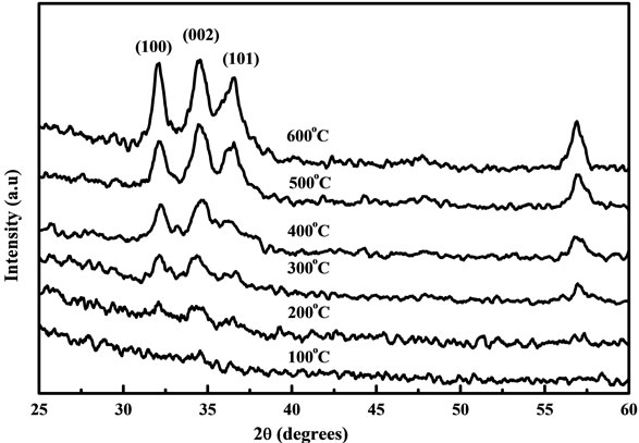
Figure 1. XRD patterns of the ZnO nanostructure prepared from fresh solution with different annealing temperatures.
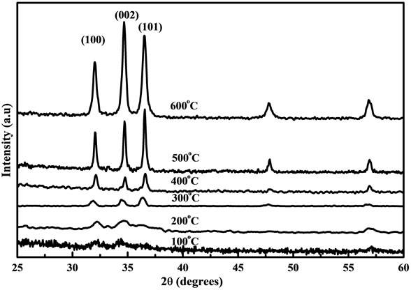
Figure 2. XRD patterns of the ZnO nanostructure prepared from two days aged solution with different annealing temperatures.
form crystal grow at 600˚C and the diffraction peaks were stronger by comparing the samples annealed from 100˚C to 500˚C. Figure 3 shows the XRD patterns of the ZnO nanostructure using (a) fresh and (b) two days aged solution annealed at 600˚C. For the samples prepared from fresh solution, the diffraction peaks such as (100), (101) and (002) are broader. But after two days aging the diffraction peaks were intense and narrow which indicates that material has good crystallinity [17] and large grain size. All the diffraction peaks from the film prepared by aged solution can be well indexed to the hexagonal phase of ZnO reported in JCDDS card (No. 36- 1451). The lower intensities and broader diffraction peaks from fresh solution samples show that the films may have finer crystalline size when compared to aged samples. The lowest (0.435˚) and highest (0.528˚) full width at half maximum (FWHM) were obtained for films made from aged and fresh solution as shown in figure 3. However the value of FWHM is inversely proportional to the grain size implying that the grain size of the samples was improved in the aged solution when compared with

Figure 3. XRD patterns of the ZnO nanostructure prepared from (a) fresh and (b) two days aged solution annealed at 600˚C.
fresh solution. The grain size of the films was calculated from the FWHM of the peak corresponding to (002) plane using Scherrer formula [18].
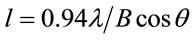
where λ is radiation wavelength (1.54 Å), B is FWHM of the diffraction peak and θ is a diffracting angle. The grain size was 15.8 and 19 nm for fresh and aged solution respectively. From the XRD results it was found that the aged solution samples are having hexagonal structure with large grain size and this leads to the improved quality of the ZnO nanostructure. The aging conditions are such that the systems will tend to reach their thermodynamic colloidal stability and this stability leads to the variations of morphology, size, or structural properties as a result of the aging mechanism [19].
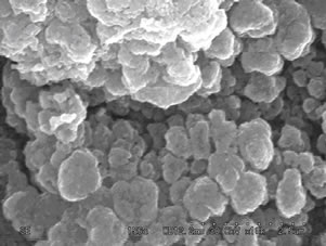
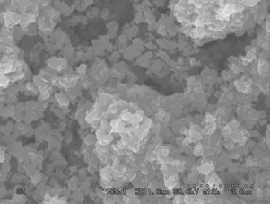
Figures 4 and 5(a)-(d) show the SEM images of ZnO nanostructure grown on glass substrates prepared from fresh and two days aged solution annealed at 300˚C, 400˚C, 500˚C and 600˚C respectively. At below 300˚C uniform crystal structure was not grown completely and poor alignment of the nanostructures was observed. This was confirmed by X-ray diffraction pattern by showing weak orientation peak at below 300˚C. When increasing the annealing temperature from 300˚C to 600˚C the nanostructure grows along the (101), (100) and (002) directions and also improved the structural alignment. From figures 4(c) and 5(c), it is observed that the crystal started to grow on the surface which is perpendicular to the substrate. The ZnO films prepared from fresh solution and annealed at 600˚C shows that the grains sizes are large and no evidence for hexagonal structure of the ZnO nanostructure as shown in figure 4(d). In figure 5(d), the sample shows hexagonal structure and it confirms that the films are indexed to the hexagonal phase of ZnO. These results agree well with the X-ray results. The samples annealed at 600˚C using two days aged solution
 (a)
(a)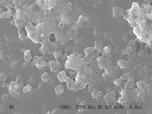 (b)
(b) (c)
(c)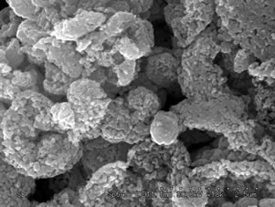 (d)
(d)
Figure 4. SEM images of the ZnO nanostructure prepared from fresh solution with different annealing temperature of (a): 300˚C; (b): 400˚C; (c): 500˚C; (d): 600˚C.
 (a)
(a)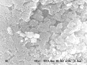 (b)
(b)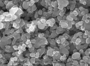 (c)
(c) (d)
(d)
Figure 5. SEM images of the ZnO nanostructure prepared from two days aged solution with different annealing temperature of (a): 300˚C; (b): 400˚C; (c): 500˚C; (d): 600˚C.
gives the same wurtzite ZnO patterns with high intensity of diffraction peaks which provides further evidence that the aged solution has little influence on the orientation of the ZnO nanostructure.
Raman spectrum is an effective method to investigate the crystallization, structure and defects in the nanostructure materials. Wurtzite ZnO belongs to the C46V space group with two formula units per primitive cell. Figures 6 and 7 show the Raman spectra of ZnO nanostructure grown at temperatures ranging from 100˚C to 600˚C using fresh and two days aged solution. There is no variation observed for the samples annealed at 100˚C to 300˚C as shown in figures 6 and 7. When samples are annealed
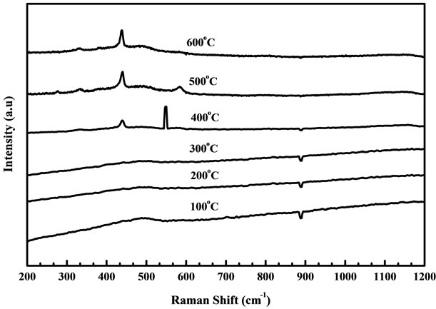
Figure 6. Raman spectra of ZnO nanostructure prepared from fresh solution with different annealing temperatures.

Figure 7. Raman spectra of ZnO nanostructure prepared from two days aged solution with different annealing temperatures.
at 400˚C to 600˚C, the peak at 437 cm−1 was observed which leads to the ZnO nonpolar optical phonon (E2) modes and it is an assigned Raman peak of ZnO bulk [20]. The peak at 330 cm−1 assigned to the Raman spectrum arising from zone boundary phonons 3E2H-E2L (multiphonon), while the peak at 561 cm−1 leads to the E1 (LO) mode of ZnO associated with oxygen deficiency [21]. The samples grown at higher temperature exhibit a very low oxygen vacancy and this may be due to influence of change in particle size annealed at high temperature [22]. However when samples are annealed in air, excess zinc in the film becomes oxidized, the impurity states disappear and the magnitude of resonance Raman enhancement of the E1 (LO) mode is diminished. The peak intensity of optical phonon mode E2 is increased slightly when increasing the annealing temperature from 400˚C to 600˚C for the samples prepared from fresh solution but in two days aged solution the intensity of E2 mode is largely increased when compared with fresh solution. Figure 8 shows the Raman spectra of ZnO films obtained from (a)
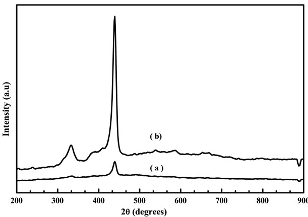
Figure 8. Raman spectra of ZnO nanostructure prepared from (a) fresh and (b) two days aged solution annealed at 600˚C.
fresh and (b) two days aged solution annealed at 600˚C. Samples prepared from aged solution indicate the most intense peak at 437 cm−1 when compared with fresh solution, which corresponds to the vibrational mode of E2 (high). The E2 mode corresponds to the band characteristics for the wurtzite hexagonal plane of ZnO. The highest intensity and narrower spectral width of the Raman active E2 mode indicated that the as-grown ZnO have good quality with a hexagonal wurtzite crystal phase. From this result, it is confirmed that the ZnO nanocrystals possibly gives the better crystal quality and less impurity when using the two days aged solution instead of using a fresh solution.
Figures 9 and 10 show the PL spectra of the samples prepared from fresh and two days aged solution annealed at 400˚C, 500˚C and 600˚C. In figure 9 the UV emission was not observed clearly for samples annealed from 400˚C and 500˚C. When samples annealed at 600˚C the broad luminescence band was observed around 470 nm other than the weak UV emission. However the aged solutions do not exhibit this luminescence band. Detlef et al., [23] reported that the freshly prepared ZnO colloidal suspension exhibit a single broad fluorescence band with initial maximum around 460 nm. From this we can understand that the broad band around 470 nm may be due to the blue shift of fresh colloidal suspension of ZnO. The results of PL spectra may prove that the solution condition has a little influence on the ZnO nanostructure. All the spectra from aged solution have a UV emission around 383 nm and visible emission around 530 nm, which is generally discussed with respect to oxygen vacancies at the surface. The UV band emission of ZnO has been well demonstrated to the near band-edge transition, namely the recombination of free excitons through exciton-exciton emission process [24]. In figure 10 the samples annealed at 400˚C shows that the UV emission peak which is almost equal to the green band emission. This
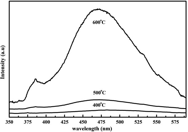
Figure 9. PL spectra of the ZnO nanostructure prepared from fresh solution with different annealing temperatures measured at room temperature.
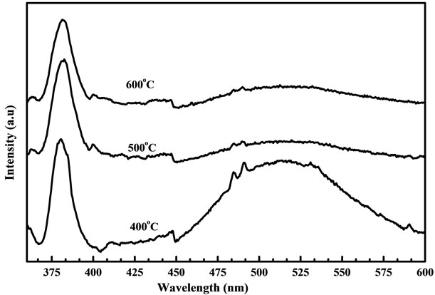
Figure 10. PL spectra of the ZnO nanostructure prepared from two days aged solution with different annealing temperatures measured at room temperature.
proves that these samples do not have good crystalline quality as they have many oxygen vacancies. But in the case of sample annealed at 500˚C and 600˚C much weaker visible emission and sharper UV peak helps to demonstrate much better optical properties. The green PL has been observed in the ZnO nanocrystals grown by hydrothermal, CVD and electrochemical methods and its origin are commonly attributed to the photo generated holes with singly ionized oxygen vacancies. However the PL spectrum of ZnO nanocrystals array is depending on the growth temperature. The band edge PL intensity increases greatly and the intensity of green PL decreases a lot when increasing the annealing temperature from 500˚C to 600˚C. Increasing the growth temperature will improve the crystal quality of ZnO nanostructure to a certain extent [25]. Although the reason for the growth temperature dependent PL is not quiet clear when related to the formation mechanism of oxygen vacancies. From the PL results it was observed that samples annealed at 600˚C gives a strong UV peak and much lower green
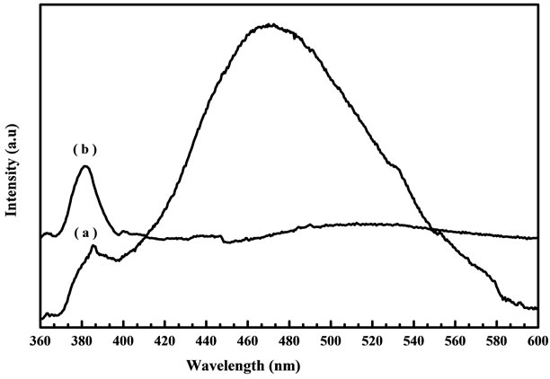
Figure 11. PL spectra of the ZnO nanostructure prepared from (a) fresh and (b) two days aged solution annealed at 600˚C.
peak when compared with samples annealed at 400˚C and 500˚C. Figure 11 shows the PL spectra measured at room temperature for (a) fresh and (b) two days aged solution annealed at 600˚C. From aged solution a strong and high intensity peak around 383 nm in the UV region and week band around 530 nm in the visible region was observed. The strong room temperature UV emission of aged solution should be attributed to the high purity, good crystallinity of the as synthesized ZnO nanostructure. It has been reported that the improvement in the crystal quality may cause the appearance of a sharp and strong UV emission and a suppressed and week green emission [26]. The PL result indicates that the optical properties of ZnO nanostructure were improved by the aged solution when compared with fresh solution.
4. Conclusion
The success of this work is that the nanostructure of ZnO has been prepared at low cost by a simple solution method. This method is based on a simple procedure and doesn’t need template supporting which leads to the formation of ZnO nanostructure. A systematic study of this work reveals that the use of aged sol-gel solution along with growth parameters will lead to the formation of ZnO nanostructure with low oxygen vacancy defect density, which might find potential applications in nanodevices. The annealing temperature plays a crucial role for the improvement of ZnO nanostructure. For the samples annealed below 300˚C, the crystal growth is non-crystalline and incomplete with poor orientations. The samples prepared by two days aged solution exhibit stronger UV emission than broad green emission, which indicates that the high optical quality of the ZnO nanostructures is prepared from aged solution. It is worthy to note that the aging mechanisms have a great influence on the formation of good quality ZnO nanostructure.
5. Acknowledgements
This work was supported by the Center for Social Contribution and Collaboration (C-SoCC), Nagoya Institute of Technology, Nagoya, Japan and FONDECYT No: 1130916, Government of Chile, Santiago, Chile.
REFERENCES
- A. M. Morales and C. M. Lieber, “A Laser Ablation Method for the Synthesis of Crystalline Semiconductor Nanowires,” Science, Vol. 279, No. 5348, 1998, pp. 208-211. doi:10.1126/science.279.5348.208
- D. C. Look, “Recent Advances in ZnO Material and Devices,” Materials Science and Engineering: B, Vol. 80, No. 1, 2001, pp. 383-387. doi:10.1016/S0921-5107(00)00604-8
- Y. Li, G. W. Meng, L. D. Zhang and F. Phillip, “Ordered Semiconductor ZnO Nanowires Arrays and Their Photoluminescence Properties,” Applied Physics Letters, Vol. 76, No. 15, 2000, pp. 2011-2013. doi:10.1063/1.126238
- R. S. Wagner and W. C. Ellis, “Vapor-Liquid-Solid Mechanism of Single Crystal Growth,” Applied Physics Letters, Vol. 4, No. 5, 1994, pp. 89-90. doi:10.1063/1.1753975
- Y. Xia, P. Yang, Y. Sun, Y. Wu, B. Mayers, B. Gates, Y. Yin, F. Kim and H. Yan, “One Dimensional Nanostructures; Synthesis, Characterization, and Applications,” Advanced Materials, Vol. 15, No. 5, 2003, pp. 353-389. doi:10.1002/adma.200390087
- Z. S. Wu, S. Z. Deng, N. S. Xu, J. Chen, J. Zhou and J. Chen, “Single Wall Carbon Nanotube Atomic Force Microscope Probes,” Applied Physics Letters, Vol. 80, No. 20, 2002, pp. 3829-3831. doi:10.1063/1.1476703
- J. Liu, X. M. Meng, Y. Jiang, C. S. Lee, I. Bello and S. T. Lee, “Gallium Nitride Nano Wires Doped with Silicon,” Applied Physics Letters, Vol. 83, No. 20, 2003, pp. 4241- 4243. doi:10.1063/1.1628820
- Y. F. Chan, X. F. Duan, S. K. Chan, I. K. Sou, X. X. Zhang and N. Wang, “ZnSe Nanowires Epitaxially Grown on Gap (111) Substrates by Molecular Beam Epitaxy,” Applied Physics Letters, Vol. 83, No. 13, 2003, pp. 2665- 2667. doi:10.1063/1.1615293
- M. H. Huang, S. Mao, H. Feick, J. Q. Yan, Y. Y. Wu, H. Kind, E. Weber, R. Russo and P. D. Yang, “Room-Temperature Ultraviolet Nanowires Nanolasers,” Science, Vol. 292, No. 5523, 2001, pp. 1897-1899.
- T. Xu, C. S. Xie and Prog, “Tetrapod–Like Nano-Particle ZnO/Acrylic Resin Composite and Its Multi-Function Property,” Progress in Organic Coatings, Vol. 46, No. 4, 2003, pp. 297-301. doi:10.1016/S0300-9440(03)00016-X
- B. L. Zhu, D. W. Zeng, J. Wu, W. L. Song and C. S. Xie, “Synthesis and Gas Sensitivity of In-Doped ZnO Nanoparticles,” Journal of Materials Science: Materials in Electronics, Vol. 14, No. 8, 2003, pp. 521-526. doi:10.1023/A:1023989304943
- A. Sekar, S. H. Kim, A. Umar and Y. B. Hahn, “Catalyst Free Synthesis of ZnO Nanowires on Si by Oxidation of Zn Powder,” Journal of Crystal Growth, Vol. 277, No. 1-4, 2005, pp. 471-478. doi:10.1016/j.jcrysgro.2005.02.006
- W. L. Hughes and Z. L. Wang, “Nanobelts as Nanocantilevers,” Applied Physics Letters, Vol. 82, No. 14, 2003, pp. 2886-2888. doi:10.1063/1.1570497
- J. Yu. Lao, J. G. Wen and Z. F. Ren, “ Hierarchical ZnO Nanostructure,” Nano Letters, Vol. 2, No. 11, 2002, pp. 1287-1291. doi:10.1021/nl025753t
- S. Lib, Y. S. Chu, D. Z. Shen, Y. M. Lu, Y. J. Zhang and X. W. Fan, “High Quality ZnO Thin Films Grown,” Journal of Applied Physics, Vol. 91, No. 1, 2002, pp. 501-505. doi:10.1063/1.1415545
- L. L. Wu, Y. S. Wu and W. Lu, “Preparation of ZnO Nanorods and Optical Characterizations,” Physica E, Vol. 28, No. 1, 2005, pp. 76-82. doi:10.1016/j.physe.2005.02.005
- Y.-H. Ni, X.-W. Wei, J.-M. Hong and Y. Ye, “Hydrothermal Preparation and Optical Properties of ZnO Nanorods,” Materials Science and Engineering: B, Vol. 121, No. 1-2, 2005, pp. 42-47. doi:10.1016/j.mseb.2005.02.065
- J.-H. Lee, B.-W. Yeo and B.-O. Park, “Effects of the Annealing Treatment on Electrical and Optical Properties of ZnO Transparent Conduction Films by Ultrasonic Spraying Pyrolysis,” Thin Solid Films, Vol. 457, No. 12, 2004, pp. 333-337. doi:10.1016/j.tsf.2003.09.075
- E. Hosono, S. Fujihara and T. Kimura, “Synthesis, Structure and Photoelectrochemical Performance of Micro/Nano Textured ZnO/Eosin y Electrodes,” Electrochimica Acta, Vol. 49, No. 14, 2004, pp. 2287-2293. doi:10.1016/j.electacta.2004.01.009
- X. L. Xu, S. P. Lau, J. S. Chen, G. Y. Chen and B. K. Tay, “Polycrystalline ZnO Thin Films on Si (100) Deposited by Filtered Cathodic Vaccum Arc,” Journal of Crystal Growth, Vol. 223, No. 1-2, 2001, pp. 201-205. doi:10.1016/S0022-0248(01)00611-X
- G. J. Exarhos and S. K. Sharma, “Influence of Processing Variables on the Structure and Properties of ZnO Films,” Thin Solid Film, Vol. 270, No. 1-2, 1995, pp. 27-32. doi:10.1016/0040-6090(95)06855-4
- A. K. Pradhan, K. Zhang, G. B. Louttus, U. N. Roy, Y. Cui and A. Burger, “Structural and Spectroscopic Characteristics of ZnO and ZnO: Er3+ Nanostructure,” Journal of Physical and Condensed Matterials, Vol. 16, No. 39, 2004, pp. 7123-7130.
- Y. C. Kong, D. P. Yu, B. Zhang, W. Fang and S. Q. Feng “Ultraviolet-Emitting ZnO Nanowires Synthesized by a Physical Vapor Deposition Approach,” Applied Physics Letters, Vol. 78, No. 4, 2001, pp. 407-409. doi:10.1063/1.1342050
- W. Detlef, Bahnemann, C. Kormann and M. R. Hoffmann, “Preparation and Characterization of Quantum Size Zinc Oxide: A Detailed Spectroscopic Study,” Physical Chemistry, Vol. 91, No. 14, 1987, pp. 3789-3798. doi:10.1021/j100298a015
- C.-H. Hung and W.-T. Whang, “A Novel Low-Temperature Growth and Characterization of Single Crystal ZnO Nanorods,” Materials Chemistry and Physics, Vol. 82, No. 3, 2003, pp. 705-710. doi:10.1016/S0254-0584(03)00331-6
- D. M. Bagnall, Y. F. Chen, Z. Zhu, T. Yam, S. Koyama, M. Y. Shen and T. Goto, “High Temperature Excitonic Stimulated Emission from ZnO Epitaxial Layers,” Applied Physics Letters, Vol. 73, No. 81, 1998, pp. 1038-1040. doi:10.1063/1.122077
NOTES
*Corresponding author.