Open Journal of Antennas and Propagation
Vol.1 No.2(2013), Article ID:37170,7 pages DOI:10.4236/ojapr.2013.12004
Finite Element Modeling and Design of Rectangular Patch Antenna with Different Feeding Techniques
![]()
1Department of Electronics & Communication, SSCET, Pathankot, India; 2Department of Electronics & Communication, BCET, Pathankot, India; 3Department of Physics and Electronics, University of Jammu, Jammu, India.
Email: *snp09arya@gmail.com, *sandeeparya@jammuuniversity.in
Copyright © 2013 Rajat Arora et al. This is an open access article distributed under the Creative Commons Attribution License, which permits unrestricted use, distribution, and reproduction in any medium, provided the original work is properly cited.
Received June 4th, 2013; revised July 10th, 2013; accepted July 20th, 2013
Keywords: Microstrip Patch Antenna; Finite Element Method; T Shaped; Feeding Point; Far Field Domain
ABSTRACT
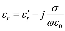
The finite element modeling of three dimensional structures is important for researchers especially in the field of antennas and other domains of electromagnetic waves. This paper presents a finite element calculations and numerical analysis for the microstrip patch antennas. In this paper, two different designs have been modelled and analyzed and both designs are based on the rectangular patches. The feeding point of one design is inside the patch while the other design contains feeding point outside the patch is T shaped. The computational analysis showed some interesting results for radiation pattern and far field domain. For these designs, the characteristic impedance taken is 50 Ω and the operating frequency domain is 1.4 to 1.7 GHz. The microstrip patch antennas are encapsulated in the inert spherical atmosphere of 20 mm thickness containing air inside it.
1. Introduction
The application of patch antennas is significant in modern era of wireless communication systems due to its light weight, small size, easy installation, and is economical [1]. Microstrip patch antenna has wide range of applications in satellite communications including cell phones as well as for defence applications [2-4]. The patch antenna creates a specific conductive structure in the environment. The exclusive property of the microstrip patch antenna is its two dimensional structure [5]. The Patch antenna provide better gain performance as compared to the traditional dipole or monopole antennas utilized in the past [6,7]. The single element resonant design of microstrip patch antenna comprises of four components, i.e., patch, ground plane, substrate, and the feeding point [8]. The conducting patch is separated from ground plane by the dielectric substrate. The patch antenna requires a small capacity structure while mounting. Different shapes of microstrip patch antennas are possible depending on the characteristics requirement like the bandwidth, gain and efficiency for a specific application [9,10]. The most demanding frequency range for antenna applications is in-between 1 to 6 GHz.
Several numerical simulation methods have been used to design microstrip structures of a patch antenna. These methods are finite difference time domain (FDTD), transmission line matrix (TLM), finite element method (FEM), and method of moments (MoM) [11-14]. Several adjustments have been reported to increase antenna bandwidth that includes an increase in substrate thickness, use of a low dielectric substrate, various impedance matching and feeding techniques [15,16]. In this paper, two different designs of rectangular patch antennas are modeled and analyzed using finite element method. Both the designs were analyzed at the same operating frequency and the behaviour of far field domain and the polar graph indicating radiation patterns were observed. The results were concluded by the comparison between the two modeled designs. The next section of the paper provides the mathematical analysis for the microstrip patch antennas using finite element method. The subsequent sections of the paper describe the design and modelling of an antenna. Sections 5 and 6 explain the results obtained after computing the design and the conclusion of this work respectively.
2. Finite Element Modelling
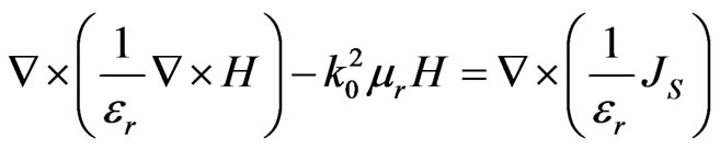
Finite element modelling (FEM) is a powerful computational technique to attain the solution of differential and integral equations. The given domain can be viewed as a set of simple geometric entities called finite elements that generate the approximation functions [17]. The FEM technique discretizes the problem by finite elements that are quadrangle or triangle for solving two dimensional problems, and tetrahedral, hexahedral or prism elements for solving three dimensional problems [18]. FEM models provide good results in quick time with accurate solutions by solving multiple differential equations using piecewise approximation [19]. The accuracy can be improved with first-order nodal basis functions and their edge elements basis [20]. For 3D modelling of a microstrip patch antenna, the time harmonic vector wave equations are used. Since antenna deals with electromagnetic waves, Maxwell’s equations [21] are to be considered for obtaining the vector wave equations and illustrated as below.
 ,and ,

where, 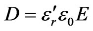 , and
, and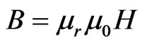 .
.
In the above equations, H is the magnetic field intensity, E is the electric field intensity and ω is the operating frequency. Also, ε0 and μ0 is the permittivity and permeability of free space, whereas, εr and μr are the relative permittivity and relative permeability respectively. The vector wave equation for E and H is given by
 and
and
where JS is the current source,
 and
and 
where k0 is the wave number of the free space [21].
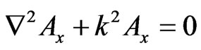
Let us consider the dimensions of the substrate such that the height of substrate h is very small in comparison to the wavelength λ within the dielectric. Thus, the field variation along the height is considered as constant due to very small substrate height. Since, the electric field is normal to the surface of the patch, hence, only transverse magnetic (TM) mode is considered. Hence the electric field will be normal to the surface of the ground plane. The top and bottom walls of the patch are perfectly electric conducting layers and the four side walls will be perfectly conducting magnetic walls. Let  is the dielectric constant of the substrate and is smaller than the edges of the patch. The homogenous wave equation for the vector potential Ax is given by
The solution for this equation using the separation of variables is given as
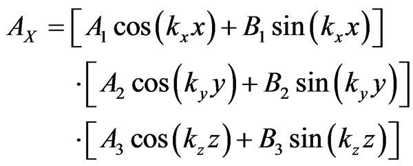
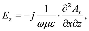
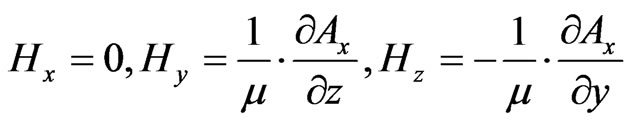
where kx, ky and kz are the wave numbers along the x, y and z direction respectively. These can be determined using boundary conditions. The electric and magnetic field related to the vector potential Ax is given by


Another important parameter for finite element analysis is the scattering parameter and this can be extracted using reflection coefficient S11 from the calculated electric field [21-23]. Thus the input impedance can be calculated as
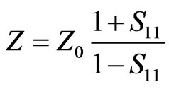
where Z0 is the characteristic or the matching impedance.
3. A Parametric Study
Some important antenna parameters can be calculated by the transmission line method [7,12] and is explained as below.
3.1. Patch Width
Numerically, the width of the microstrip patch can be calculated using the equation as [24]
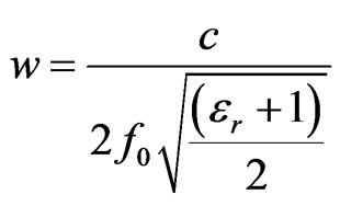
where c is the velocity of light in free space, f0 is the resonant frequency and  is the dielectric constant of the substrate.
3.2. Patch Length
The length of the patch can be calculated only if the effective dielectric constant is known [25], and the effective dielectric constant can be calculated as
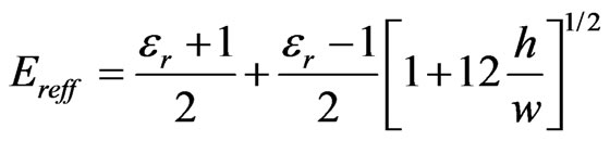
where  is the effective dielectric constant,
  is the dielectric constant of substrate, h is the height of dielectric substrate and w is the width of the patch. The dimensions of the patch is extended on each end by a distance
  and is calculated by
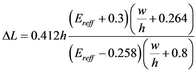
The actual length L of the patch is given as
3.3. Input Impedance
The input impedance can be obtained by the equation [12]
where Xf is the desired input impedance of the coaxial cable and Ereff is the effective dielectric constant. Similarly, the admittance can be found using the equation

3.4. Ground Dimensions
For practical design, it is necessary to have some finite ground plane. For optimum design of small patch antenna, it is required that the ground plane should be greater than the patch dimensions by approximately six times the substrate thickness all around the fringe [7]. Hence, the ground plane dimensions would be given as


3.5. Return Losses
Return losses depend upon the scattering parameters and for N = 1, S-matrix consists of a single term S11 known as reflection coefficient [26]. The magnitude of S11 can be expressed in decibels and the return losses can be estimated as
The reflection coefficient is given by
where ZS is the impedance toward the source and ZL is the impedance toward the load. The following equation can be used to calculate the input impedance of rectangular microstrip antenna.
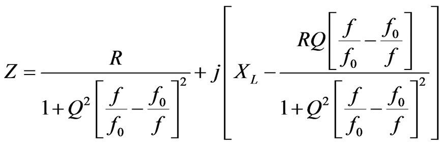
where R is the resistance of the resonant parallel RLC circuit, f0 is the resonant frequency, and Q is the quality factor associated with system losses including radiation, the loss due to heating in the conducting elements and the ground plane, and the loss due to heating within the dielectric medium [26].
3.6. Quality Factor
The quality factor is given as,

where c is the velocity of light in free space, Ereff is the effective dielectric constant, f0 is the resonant frequency and h is the height if the patch. The above quoted physiccal parameter equations for antenna design is used to set the input parameters of the microstrip patch antenna [26].
4. Modeling and Design
The two different models were designed using a electromagnetic waves (EMW), frequency domain solver. Both the model structures, i.e., rectangular and T-shaped patches are shown in Figures 1 and 2 respectively.
Both the designed antennas were enclosed in the spherical domain of diameter 85 mm and the layer thickness of the sphere was 20 mm. The material selected inside the spherical domain is air. Thus the antennas were designed and analyzed for operating in the air or atmosphere. Another reason to enclose the antenna in a spherical air domain surrounded by a perfectly matched layer (PML) is to absorb the radiation from the antenna with minimum reflection.
The dimensions of the selected materials for microstrip patch antennas design are shown in Tables 1 and 2. Table 1 shows the dimensions of microstrip patch antenna with stub i.e., the boundary from where frequency has been feed inside it while Table 2 has feeding point outside the patch.
Thermoset material is opted for substrate and microstrip patch design as it has low dielectric value. More-
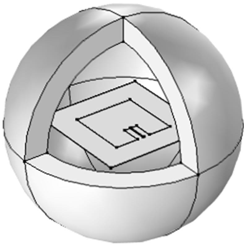
Figure 1. Rectangular patch antenna in spherical domain.

Figure 2. T-shaped patch enclosed in spherical domain.
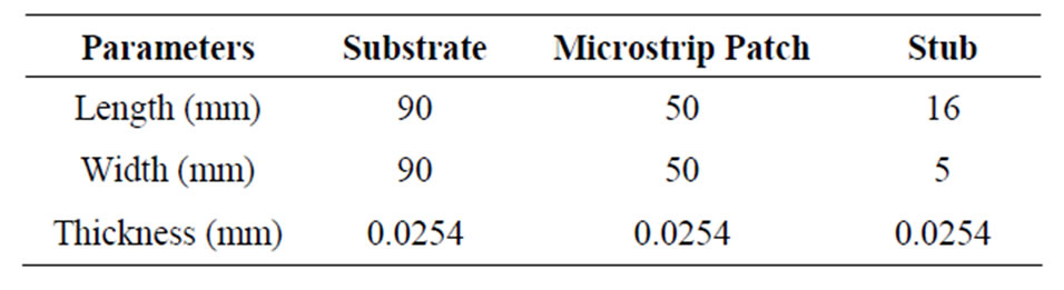
Table 1. Dimensions for rectangular microstrip patch.
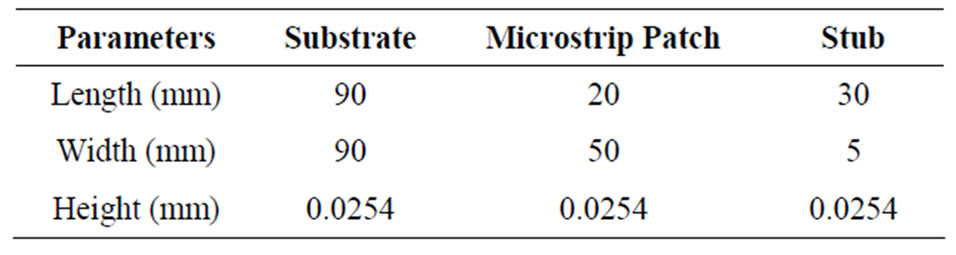
Table 2. Dimensions for T-shaped microstrip patch.
over, thermoset resins undergo a chemical change during moulding and can never again be softened by reheating. The molding compound used in semiconductors and integrated circuits (IC). Thermosetting resins are made from a mixture of monomers which react to form a large macromolecular network. They are used in diverse fields such as aerospace technology and as adhesives.
The main thermosetting systems used are phenol-formaldehyde, urea-formaldehyde, polyurethanes polyesters and epoxy resins. In our design epoxy resin has been used with tensile strength 80 N/mm2 and 20 GN/m2 value of Young’s modulus.
The material properties selected for both the designs are same and is shown in Table 3. The material chosen for the substrates and the patches are same. The operating frequency range applied to the lumped port is in-between 1.4 to 1.7 GHz. The width of the cutout region, W, is chosen to be large enough to attain minimal coupling between the antenna and the microstrip, but not so large as to significantly affect the antenna characteristics. The length of the microstrip line, L, is chosen to minimize the reflected power, S11.
5. Results and Discussions
Figure 3 shows the meshing design of a t-shaped patch antenna. For the large domain computation, tetrahedral meshing is preferred. The maximum element size selected is 37. The design was simulated on the computational machine having 3.2 GHz processor speed. The virtual memory used while simulation was 2.3 GB. Higher element size is selected to reduce the computational load and to attain the convergence plot.

Table 3. Material Parameters for selected materials.
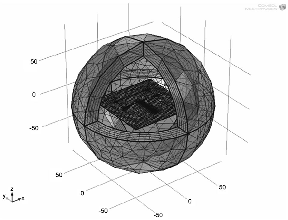
Figure 3. Tetrahedral meshing of T-shaped patch antenna.
Mesh settings give a mesh that is sufficiently fine in most parts of this design, including the minimum required 2 - 3 second-order elements across the thickness of the PML. To improve more accuracy in the results, finer mesh size are recommended where the field gradients are steep, like, on the patch and the ports. Figures 4 and 5 showed the far field domain for the rectangular microstrip patch antenna and the T-shaped patch antenna respectively.
This is clear that the maximum far field domain for the rectangular microstrip patch antenna is 1.6803 V/m while the maximum far field domain for the T-shaped microstrip patch antenna is 0.0421 V/m.
Figures 6 and 7 shows the plots of polar graph showing electric and magnetic field radiated in the surroundings for the rectangular microstrip patch antenna and the T shaped patch antenna. The beam of the antenna should be very sharp and thus increases the performance in propagating signals. The polar plot for the t-shaped antenna shows formation of some standing waves and this

Figure 4. Far field domain for rectangular patch antenna.

Figure 5. Far field domain for T-shaped patch antenna.

Figure 6. Polar graph plot for rectangular patch antenna.
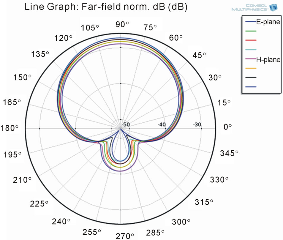
Figure 7. Polar graph plot for T-shaped patch antenna.
leads to the return losses. Figures 8 and 9 show the variation in return losses to the domain of frequencies applied to the rectangular patch and the T-shaped patch antenna respectively.
The high value of return loss means that the reflection wave return back to the source is very small and the amount of radiation power is very high. This characteristic is very important in radiator devices such as antennas. From the graphs obtained for return losses clearly indicates that the resonant frequency for the rectangular microstrip patch antenna is 1.6 GHz.
Figure 9 shows that the return loss continuously decreasing with the increase in frequency for T-shaped antenna. All these result shows that the variation of the parameters changes the resonance frequencies of the antenna. Hence, there are several parameters that should be optimized to attain proper performance.
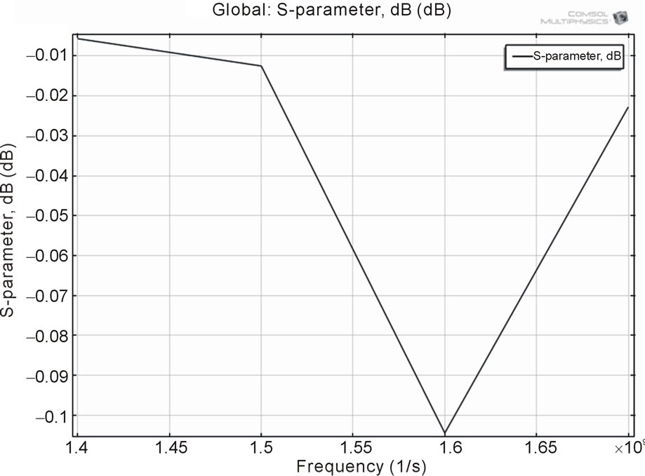
Figure 8. Return loss versus frequency for rectangular patch antenna.

Figure 9. Return loss versus frequency for T-shaped patch antenna.
6. Conclusions and Future Scope
This paper proposes two different microstrip patch antenna designs that are modest and economical for mobile communication applications. The designs have been simulated for obtaining far-field radiations, polar plots and the insertions losses and the characteristics of two different microstrip patch antennas. The comparison shows that the results for rectangular patch antennas in terms of radiation pattern, far field domain and the resonant frequency obtained from the return loss are better than the T-shaped microstrip patch antenna.
Future work implies the enhancement techniques for the bandwidth and radiation patterns of these antennas. Designs using different substrate and structure can be taken into consideration for the future research. Different patches, dimensions and feeding techniques may also affect the performance of the antennas.
REFERENCES
- G. A. Dalli, L. Zenkouar and S. Bri, “Comparison of Circular Sector and Rectangular Patch Antenna Arrays in C-Band,” Journal of Electromagnetic Analysis and Applications, Vol. 4, No. 11, 2012, pp. 457-467. doi:10.4236/jemaa.2012.411064
- J. Singh, A. P. Singh and T. S. Kamal, “On the Design of Triangular Microstrip Antenna for Wireless Communication,” International Journal of Computer Applications, Vol. 1, 2011, pp. 103-106.
- S. Arya, S. Khan, C. K. Shan and P. Lehana, “Design of a Microstrip Patch Antenna for Mobile Wireless Communication Systems,” Journal of Computational Intelligence and Electronic Systems, Vol. 1, No. 2, 2013, pp. 1-5.
- D. M. Elsheakh and E. A. Abdallah, “Different Feeding Techniques of Microstrip Patch Antennas with Spiral Defected Ground Structure for Size Reduction and Ultra-Wide Band Operation,” Journal of Electromagnetic Analysis and Applications, Vol. 4, No. 1, 2012, pp. 410- 418. doi:10.4236/jemaa.2012.410056
- J. Mondal and S. K. Ray, “Design Smart Antenna by Microstrip Patch Antenna Array,” International Journal of Engineering and Technology, Vol. 3, No. 6, 2011, pp. 675-682.
- A. K. Gupta, R. K. Prasad and D. K. Srivastava, “Design and Development of Dual E-Shaped Microstrip Patch Antenna For Bandwidth And Gain Enhancement,” International Journal of Electronics and Communication Engineering & Technology, Vol. 3, No. 3, 2012, pp. 34-42.
- K. O. Odeyemi, D. O. Akande and E. O. Ogunti, “Design of an S-Band Rectangular Microstrip Patch Antenna,” European Journal of Scientific Research, Vol. 55, No. 1, 2011, pp. 72-79.
- S. H. Al-Charchafchi, W. K. Wan Ali, M. R. Ibrahim and S. R. Barnes, “Design of a Dual Patch Triangular Microstrip Antenna,” Applied Microwave & Wireless, 1998, pp. 60-67.
- B. Garg, A. Samadhiya and R. D. Verma, “Analysis and Design of Microstrip Patch Antenna Loaded with Innovative Metamaterial Structure,” Research Journal of Physical and Applied Science, Vol. 1, No. 1, 2012 pp. 13-19,.
- Z. N. Chen, “Wideband Microstrip Antennas with Sandwich Substrate,” IET Microwaves, Antennas & Propagation, Vol. 2, No. 6, 2008, pp. 538-546. doi:10.1049/iet-map:20070284
- S. Singh, N. Agarwal, N. Nitin and A. K. Jaiswal, “Design consideration of Microstrip Patch Antenna,” International Journal of Electronics and Computer Science Engineering, Vol. 2, No. 1, 2012, pp. 306-316.
- S. Arya, S. Khan, C. K. Shan and P. Lehana, “Design of Small Integrated Antenna for Peer to Peer Wireless Communication,” International Journal of Mobile Network Communications & Telematics, Vol. 2, No. 3, 2012, pp. 11-20.
- G. Cakir and L. Sevgi, “Design, Simulation and Tests of a Low-cost Microstrip Patch Antenna Arrays for the Wireless Communication,” Turkish Journal of Electrical Engineering, Vol. 13, No. 1, 2005, pp. 93-103. doi:10.5121/ijmnct.2012.2302
- M. T. Islam, M. N. Shakib and N. Misran, “Broadband Microstrip Patch Antenna,” European Journal of Scientific Research, Vol. 27, No. 2, 2009, pp. 174-180.
- M. N. Srifi, M. Meloui and M. Essaaidi, “Rectangular Slotted Patch Antenna for 5 - 6 GHz Applications,” International Journal of Microwave and Optical Technology, Vol. 5, No. 2, 2010, pp. 52-57.
- R. Alsulami and H. Song, “Double-Sided Microstrip Circular Antenna Array for WLAN/WiMAX Applications,” Journal of Electromagnetic Analysis and Applications, Vol. 5, No. 4, 2013, pp. 182-188. doi:10.4236/jemaa.2013.54029
- J. S. Wang, “Finite Element Computation of Antenna Impedance Including Feed Modeling,” IEEE Transactions on Magnetics, Vol. 33, No. 2, 1997, pp. 1500-1503. doi:10.1109/20.582545
- Z. Polik, “Fractal Based Antenna Size Reduction Examined by Numerical Methods,” Acta Technica Jaurinensis, Vol. 4, No. 3, 2011, pp. 393-411.
- M. Surita and A. Marwaha, “Finite Element Analysis for Optimizing Antenna for Microwave Coagulation Therapy,” Journal of Engineering Science and Technology, Vol. 7, No. 4, 2012, pp. 462-470.
- X. Rui and J. Hu, “Higher Order Finite Element Method For In Homogeneous Axisymmetric Resonators,” Progress in Electromagnetics Research B, Vol. 21, 2010, pp. 189-201.
- C. A. Balanis, “Antenna Theory: Analysis and Design,” 2nd Edition, John Wiley and Sons, NewYork, 1997.
- M. H. Ullah, M. T. Islam and J. S. Mandeep, “A Parametric Study of High Dielectric Material Substrate for Small Antenna Design,” International Journal of Applied Electromagnetics and Mechanics, Vol. 41, No. 2, 2013, pp. 193-198.
- S. K. Patel and Y. P. Kosta, “Size Reduction in Microstrip Based Meandered Radiating Structure Using Artificial Substrate,” International Journal of Applied Electromagnetics and Mechanics, Vol. 41, No. 2, 2013, pp. 207-216.
- J. R. James and P. S. Hall, “Handbook of Microstrip Antennas,” Peter Peregrinus, London, 1985.
- D. M. Pozar, and D. H. Schaubert, “Microstrip Antennas, the Analysis and Design of Microstrip Antennas and Arrays,” IEEE Press, New York, 1995.
- C. Yildiz and K. Guney, “Simple Model for the Input Impedance of Rectangular Microstrip Antenna,” Journal of Engineering Sciences, Vol. 4, No. 3, 1998 pp. 733- 738.
NOTES
*Corresponding author.