Optics and Photonics Journal
Vol.06 No.08(2016), Article ID:69989,13 pages
10.4236/opj.2016.68022
Simulations of a Novel All-Optical Flip-Flop Based on a Nonlinear DFB Laser Cavity Using GPGPU Computing
Hossam Zoweil
Advanced Technology and New Materials Research Institute, City of Scientific Research and Technology Applications, New Borg EL-Arab City, Egypt

Copyright © 2016 by author and Scientific Research Publishing Inc.
This work is licensed under the Creative Commons Attribution International License (CC BY).
http://creativecommons.org/licenses/by/4.0/


Received 15 July 2016; accepted 21 August 2016; published 24 August 2016
ABSTRACT
A new all-optical flip-flop based on a nonlinear Distributed feedback (DFB) structure is proposed. The device does not require a holding beam. A nonlinear part of the grating is detuned from the remaining part of the grating and has negative nonlinear coefficient. Optical gain is provided by an injected electrical current into an active layer. In the OFF state, due to the detuned section, no laser light is generated in the device. An injected optical pulse reduces the detuning of the nonlinear section, and the optical feedback provided by the DFB structure generates a laser light in the structure that sustains the change in the detuned section. The device is switched “OFF” by detuning another section of the grating by a Reset pulse. The Reset pulse reduces the refractive index of that section by the generation of electron-hole pairs. The Reset pulse wavelength is adjusted such that the optical gain provided by the active layer at that wavelength is zero. The Reset pulse is prevented from reaching the nonlinear detuned section by introducing an optical absorber in the laser cavity to attenuate the pulse. The device is simulated in time domain using General Purpose Graphics Processing Unit (GPGPU) computing. Set-Reset operations are in nanosecond time scale.
Keywords:
All-Optical Flip-Flop, Bistability, DFB Laser, Urbach Tail

1. Introduction
All-optical flip-flop is required for all optical routing and processing of optical data packets [1] . All-optical routing and processing of optical data packets eliminates the need to convert the data signal from optical domain to electronics domain and vice versa, which reduces complexities and increases processing speed. All-optical flip-flop based on coupled laser diodes is investigated in [2] . All-optical flip-flop based on micro ring lasers is shown in [3] . Low power all-optical flip-flop based on a micro disk laser diode is fabricated and tested in [4] . An all optical flip-flop based on a single distributed feedback semiconductor laser is implemented in [5] , and it requires also a holding beam. A device based on vertical cavity semiconductor optical amplifier that requires a holding beam is shown in [6] . Another device based on active multi-mode interference laser diode is described in [7] . All optical flip-flop based on bistable laser diodes is discussed in [8] [9] .
In [10] , an all-optical flip-flop based on a chirped DFB laser structure was investigated. The device has bi-stable output optical mode power, and it does not require a holding beam. The chirp, in [10] , is accompanied with a gradually increasing negative nonlinear coefficient. The chirp prevents lasing at the “OFF” state (low light intensity in the structure). At high light intensity in the structure, the nonlinearity reduces the chirp along the structure, and the optical feedback from the grating allows for a laser mode to build up. The device is switched “OFF” by an optical pulse at a wavelength longer than the wavelength of the emitted laser light. This is achieved by reducing the optical gain of the emitted laser mode wavelength by cross gain modulation (XGM).
In [11] , an all-optical ip-op based on a 3-section DFB laser structure is introduced. Two sections of the DFB structure are detuned from the middle part of the DFB structure. The 2 detuned sections have optical negative nonlinearity. The device is switched “ON” by an optical pulse that reduced the detuning of both sections. When the detuning is reduced, the DFB structure provides the optical feedback required to start a laser mode. The device is switched “OFF” by XGM by an optical pulse of a lower frequency than the operating frequency. In [12] , an all-optical ip op is investigated where only one section of the DFB laser structure is detuned. However, the ip-op is switched “OFF” by an optical pulse at a frequency higher than the operating frequency by XGM.
In this work, an improved nonlinear DFB structure is introduced. The device schematic is shown in Figure 1. The wave-guiding layer consists of 3 Sections. Section “3” is a detuned nonlinear section of the DFB grating. The nonlinear detuned section prevents a laser mode from building up at a low light intensity in the structure. At high light intensity in the structure, at wavelength  that corresponds to a photon energy just below the band-gap energy in Section “3”, the detuning is decreased due to negative nonlinear coefficient. In this case, the optical feedback in the structure increases and allows for an optical laser mode to build up. The laser mode intensity maintains the reduction of the detuning of Section “3”, and the laser mode is stable. The device structure is easier to implement than the structure in [10] , because it uses a section with a constant detuning instead of a detuning that is due to a gradual change in the refractive index. The device is switched “OFF” by an optical pulse at wavelength
 . The optical pulse at
  detunes section 1 by decreasing its average refractive index, and the optical feedback along the grating is reduced. The laser mode decays, and the device is switched “OFF”. The device presented in this work has advantages over the device in [11] . In [11] , 2 nonlinear sections are needed to achieve bistability, where in this work only one nonlinear section is required. Also, in [12] , the device is switched “OFF” by XGM, but in this work, the device is switched “OFF” by detuning a section of the DFB structure, and the optical gain is not altered. In this case, the switch “OFF” dynamics is controlled

Figure 1. Device schematic, the laser mode overlaps with the grating and the active layer.
the negative optical nonlinearity process in the wave-guiding layer. The negative optical nonlinearity is achieved by direct absorption of a part of the incident light at a photon energy slightly less than the band gap energy of the semiconductor. Hence, by altering the semiconductor properties the switch “OFF” process could be controlled. In the next section, the device design and “ON/OFF” switching dynamics were described.
2. Device Description and Switching Dynamics
Figure 1 shows the schematic of the device including input signals and output laser mode. The optical gain in the device is provided by electrical current injection in the active layer Figure 1. The wave-guiding layer of the device consists of a phase shifted nonlinear grating of period . where
  is the average refractive index along the grating, and
  is the wavelength at the center of the reflection band of the grating. The device is switched “ON” by a “SET” pulse, and it is switched “OFF”, by a “RESET” pulse at a different wavelength. The grating and the negative nonlinear refractive index distribution at the laser mode wavelength
  (
( ) is shown in Figure 2. The negative nonlinear coefficient in section “3” of the nonlinear wave-guiding layer is provided by direct photon absorption at the Urbach tail, Figure 3. The absorption coefficient at Urabch tail is expressed as
 ,
,  is the band gap energy (all energies are expressed in electron. volt)
  is the direct optical loss,
  is the band-gap optical loss at
 , and
, and  is chosen to be 0.01 e.V., [13] [14] . The absorbed photons produce electron-hole pairs in the nonlinear wave- guiding section “3”. The electron-hole pairs generated reduce the refractive index at photon energy just below the band-gap energy.
At low light intensity in the structure, the optical feedback is not enough to produce a lasing mode due to a detuned part (section “3”) of the grating. When an optical pulse of a wavelength  is sent through the structure, part of the pulse energy is absorbed in section “3”, and it produces electron-hole pairs that reduce the refractive index. When the detuning of the nonlinear section is reduced, the reflection band of this section overlaps with the reflection band of the other part of the grating and more photons are reflected from section “3” to the rest of the grating. This increases the optical feedback in the structure which allows for a laser mode to build up. More photons are reflected back to sections “2” and “1” of the grating which increases optical feedback and reduces the number of photons leaving the cavity from the terminal end of the grating.
To switch the laser “OFF”, section “1” of the grating as in Figure 1 is detuned from the grating center reflection band wavelength  by generating electron-hole pairs to reduce refractive index of that section. Whence

Figure 2. Linear and nonlinear refractive index distribution at 
 .
.

Figure 3. Direct absorption loss in Section 3 (Urbach tail) and optical gain spectrum.
the section “1” is detuned, the distributed optical feedback cannot provide enough optical feedback to sustain the laser mode. The laser mode decays and the electron-hole pairs density in section “3” decreases with time. The detuning of section “3” is restored to its value in the “OFF” state. The device will remain in the “OFF” state till another optical pulse at  triggers the device “ON” again. The reduction of refractive index in section “1” is done by injecting an optical pulse of wavelength
  where
where  is just below the band gap energy in this section. In the same time,
  is chosen such that the gain of the active layer
 , Figure 3, [15] .
  is greater than
 , so it can reduce the refractive index in section “3” by generating more electron-hole pairs. To avoid this, the semiconductor band gap energy in section “2” is adjusted to provide a large absorption loss at
 , so that the photons of energy
  are absorbed in section “2” before reaching section “3”. The absorption coefficients and corresponding band gaps along the nonlinear grating are shown in Figure 4 and Figure 5. The device could be built using InGaAsP alloy on InP substrate. The band gap energies in each section could be adjusted by altering the percentage of each element of the InGaAsP semiconductor [16] . Also, the device could be built from 3 DFB laser devices, where each device has its wave-guiding layer altered as described in Figure 4 and Figure 5. In the following simulations, wavelengths are set as follow:
  and
and . In the next section a mathematical model of the device is introduced. Equations describing optical fields and electron-hole densities in the active layer and nonlinear wave-guiding layers are presented. Also, simulations parameters are tabulated.
3. Mathematical Model and Simulation Parameters
Coupled mode equations describe the optical fields in the structure [17] . Rate equations describe the electron-hole pairs density in both the active layer and the nonlinear wave-guiding layer. The “RESET” pulse is modeled by an analytic model where the power of the device decays due to an attenuation coefficient that depends on the section through which the pulse is propagating.
 .
.
The total electric field of the laser mode propagating in the device is described by a sum of a forward and backward propagating field;

Figure 4. Semiconductor band-gap along the wave-guiding layer, and Set and Reset pulses photon energies.

Figure 5. Direct absorption loss  at (a)
 , and (b)
  along the wave-guiding structure.
 .
.
The laser mode is modeled at . The “RESET” pulse was assumed a wavelength
 (1)
(1)
 (2)
(2)
 (3)
(3)
 (4)
(4)
 (5)
(5)
 (6)
(6)
 (7)
(7)
Equations (1) and (2) describe the two coupled mode equations of the two counter propagating fields. The phase shift  is zero for
  and f = p for
 . c is the light speed in vacuum, and
  is the average refractive index in the laser cavity.
 , where
  is the grating period.
 .
.  presents the detuning and the direct optical loss along the grating.
  is the change in the refractive index due to the injected electron-hole pairs density by direct absorption at photon energy slightly less than the band gap energy of the semiconductor (
 electron-Volt) [18] [19] .
The ratio between the induced loss due to electron-hole pairs generated and the change in the refractive index is . In this device model,
  for
for , and 0 otherwise.
  presents the coupling between the forward mode and the backward mode, and
 .
.  is the intrinsic cavity loss. Equation (5) presents the rate equations electron-hole pairs density in the nonlinear wave-guiding layer.
  and
and  present the direct absorption loss in the nonlinear wave-guiding layer of the laser mode and the reset pulse respectively.
  for
for  and 0 otherwise.
  for
for . For
. For ,
, . For
. For , we assumed that the pulse signal at
  has zero intensity due to absorptions at section 1 and 2, so
  is not modeled in the simulations in section “3”.
 and
and  are the power densities of the laser modes at
  (
( ), and the power density of the “RESET” pulse at
  (
( ) respectively.
  is the current injected to the active layer. q is the electron charge. V is the optical laser cavity volume. S is the photon density in the cavity at
 . Equation (6) presents the rate equation of the injected carriers density in the active layer.
The other simulation parameters are tabulated in Table 1.
In the following sections, numerical simulations of optical bistability and switching dynamics in time domain are performed. The mathematical model is solved using Fourth order Runge-Kutta technique. The length of the device is divided into 80 sections, and the time step is . The spontaneous emission optical fields are added as random signals at each integration step to the forward and backward fields. General purpose graphics processing unit (GPGPU) computing is used to accelerate the numerical simulations of the device. The length of the device is devided into 80 sections along the z direction. The integrations of the backward and forward fields along each the 80 sections are done by assigning a thread on the GPU to each section. All the integrations along the 80 sections are done in parallel to reduce the total computation time. The computation time is reduced about 15 times. NVIDIA “GTX 670” graphics processing unit is used to perform parallel computing of the forward and backward fields at each one of the 80 sections along the z direction. The code is written using CUDA C [20] .
4. Simulations Results
In all the following numerical simulations the laser mode power is normalized to  Watt. The electron-hole pairs density in the nonlinear wave-guiding layer is normalized to
 . The electron-hole pairs density of carriers injected into the active layer
  is normalized to
 .
.

Table 1. Simulation parameters.
4.1. Optical Bistability Loop
A mathematical experiment is performed to find the injected current to the laser device at which the device has 2 stable optical outputs levels at the same injected current. The injected current to the device is increased linearly with time from 0 to  Ampere in 37.5 nanosecond, then, the current decreases linearly from
  to 0 Ampere in 37.5 nanosecond. A part of the output optical power versus injected current relation is shown in Figure 6. An injected current of
  Ampere is used in all of the following simulations to insure bistable operation of the device.
4.2. OFF State and On State
Simulations of the output optical power are performed for a long simulation time to test the stability of the device output in the “OFF” state and the “ON” state. The output power of the device in the “OFF” state is simulated in the time domain for 75 nanosecond, Figure 7. To switch the device from “OFF” state to the “ON” state an optical pulse at  is injected to the device at
 . The pulse is injected at simulation time
  nanosecond. The pulse width is 0.1875 nanosecond and has a peak power of
  Watt (
 picojoule). The input optical pulse induces electron-hole pairs in section “3” on the nonlinear wave-guiding layer. The electron- hole pairs reduces the detuning of this section, the reflection band of this section overlaps with the reflection band of the rest of the grating. The number of photons reflected back from section “3” increases. The optical feedback is increased and the structure allows for a laser mode to build up. The laser mode provides photons at
 , part of these photons is absorbed in section “3” to maintain the number of electron-hole pairs in this section. The electron-hole pairs generated in section “3” maintain the change in detuning that allows the laser mode to exist.
The changes in the refractive index (normalized to ) along the structure at the end of the simulation time (at
  nanosecond) for both “ON” state and “OFF” state are shown in Figure 7. The output power in the “ON” state is shown in Figure 8. Nc at
 , and Ng at
 , are plotted in Figure 9 and Figure 10.

Figure 6. Optical bistability loop.

Figure 7. Output optical power in: (a) “OFF” state, (b) “ON” state.
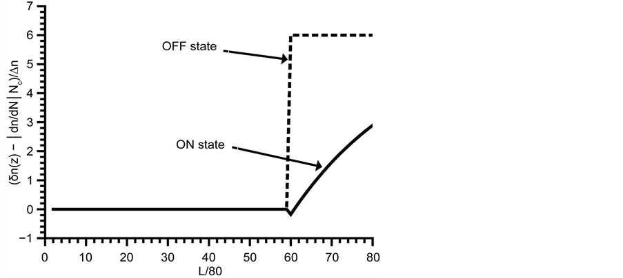
Figure 8. Normalized refractive index distribution in “OFF” state and “ON” state.
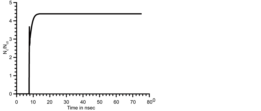
Figure 9. Normalized  in the “ON” state at
 .
.

Figure 10. Normalized  in the “ON” state at
 .
.
4.3. ON/OFF Switching Dynamics
“ON/OFF” switching dynamics are investigated in the time domain. The device is simulated for 11.25 nanosecond. At simulation time  nanosecond, an optical pulse at
  of peak power
  Watt and 0.1875 nanosecond width (
 picojoule) sets the device “ON”. At simulation time
  nanosecond, an optical pulse at
  of peak power of
  Watt and 1.875 nanosecond width (0.9375 picojoule) resets the device to the “OFF” state. The input optical power pulses are shown in Figure 11. The output optical mode is shown in Figure 12. The set pulse switches the device “ON” by generating electron- hole pairs in section “3” and the electron-hole pairs reduce the detuning of the refractive index in this section. More photons are reflected back at section “3”, and a laser mode builds up and maintains the detuning by providing electron-hole pairs in section “3”.
The “RESET” pulse switches the device “OFF”. The photons at  are absorbed in section “1” and produce electron-hole pairs. The generated electron-hole pairs reduce the average refractive index along section “1”. Hence, the reflection band of the grating section “1” does not overlap effectively with the reflection band of sections “1” and “2”. More photons escape the laser cavity through section “1”. The structure can no longer sustain a laser mode at
 . As laser mode decreases quickly inside the laser cavity,
  in section “1” decays with time and the refractive index in section “1” is restored to its value before the “SET” pulse. After the “RESET” pulse elapses, the refractive index in section “1” is restored to its value in the “OFF” state, and the

Figure 11. Input optical pulses at .
.

Figure 12. Output optical laser mode power at  during ON/OFF simulations.
device remains in the “OFF” state. Figure 13 shows  evolution with time at
  during Set/Reset operation. The evolution of
  with time at
  is shown in Figure 14. The detuning of refractive index normalized to
 ,
,  , is shown in Figure 15. The detuning at
  nano- second,
  nanosecond,
  nanosecond, and
  during the “RESET” pulse is plotted. The detuning at the end of the simulation time
  nanosecond is shown in Figure 15. The negative peak at
  corresponds to the change in refractive index due to electron-holes pairs generated by the direct absorption at the beginning of section “2”.
While the “SET” operation takes about 0.5 nanosecond to stabilize the output mode power in the “ON” state, resetting the device to the “OFF” state takes about 2 nanosecond. In the “SET” operation the input signal is amplified, while in the “RESET” operation the “RESET” pulse is not amplified. During the “RESET” operation, the “RESET” pulse does not alter  directly.
  is restored to its value in the “OFF” state due to the decrease of light intensity at
  in the optical cavity.
5. Discussion
In this work, an all-optical ip-op is simulated. The length of the device is 187:5 μm. In comparison with an

Figure 13. Electron-hole pairs density Nc at  during ON/OFF simu- lations.

Figure 14.  at
at  in the active layer during ON/OFF simulations.
another work in [10] where the device length is 375 μm. Also the operating current in this work was 0:096225 Ampere and in [10] the injected current is 0:294358 Ampere. The device simulated in this work has a shorter length and operates at a lower injection current. The Reset pulse width in [10] is 9:375 nanosecond, while in this work a Reset pulse of 1:875 nanosecond switches the device OFF. In general, the design described in this work shows fast operation compared to [10] . The device investigated in [10] requires a wave-guiding layer that increases linearly along the device. Also it requires having a direct optical loss that increases linearly with distance too. However in this device only one section of the wave-guiding layer has a slightly higher refractive index and has a direct absorption loss. Hence, in this work, the device fabrication is easier. In this work, the device is Reset by detuning part of the laser cavity which is a section of the DFB structure, and the optical gain is not altered. In [10] , the Reset pulse reduces the optical gain by cross gain modulation that switches OFF the output laser mode and allows the refractive index to return to its original distribution in the OFF state.

Figure 15. Detuning along the structure during Reset pulse and at the end of the simulation time.
6. Conclusion
An all-optical flip-flop based on a nonlinear wave-guiding layer is suggested and simulated in the time domain. The nonlinearity in the wave-guiding layer is achieved by direct absorption of photons at the Urbach tail at photons energy just below the band-gap energy of the semiconductor. The device is switched “ON” by an optical pulse of 0.1875 nanosecond width ( picojoule), and is switched “OFF” by an optical pulse of 1.875 nanosecond width (0.9375 picojoule). The switching dynamics are in nanoseconds time scale which could be useful for all optical data packet switching and routing. The device could be built using semiconductor alloy InGaAsP, where by changing the percentages of elements in the alloy the band-gap could be altered. Parallel computing using GPGPU card is used to reduce the computation time of the set of equations that describes the mathematical model of the device.
Cite this paper
Hossam Zoweil, (2016) Simulations of a Novel All-Optical Flip-Flop Based on a Nonlinear DFB Laser Cavity Using GPGPU Computing. Optics and Photonics Journal,06,203-215. doi: 10.4236/opj.2016.68022
References
- 1. https://developer.nvidia.com/cuda-zone
- 2. Hartmut, H. (1988) Optical Nonlinearities and Instabilities in Semiconductors. Academic Press, Inc., New York.
- 3. Bennett, B.R., Soref, R.A. and Del Alamo, J.A. (1990) Carrier-Induced Change in Refractive Index of InP, GaAs, and InGaAsP. IEEE Journal of Quantum Electronics, 26, 113-122.
http://dx.doi.org/10.1109/3.44924 - 4. Carrol, J., Whiteaway, J. and Plumb, D. (1998) Distributed Feedback Semiconductor Laser. IEE, London.
http://dx.doi.org/10.1049/PBCS010E - 5. Adachi, S. (2004) Physical Properties of III V Semiconductor Compounds. Wiley, New York.
- 6. Agrawal, G.P. and Dutta, N.K. (2001) Semiconductor Lasers. Kluwer Academic Publishers, US.
- 7. Dow, J.D. and Redfield, D. (1972) Toward a Unified Theory of Urbach’s Rule and Exponential Absorption Edges. Physical Review B, 5, 594-610.
- 8. Pankove, J.I. (1965) Absorption Edge of Impure Gallium Arsenide. Physical Review, 140, A2059-A2065.
http://dx.doi.org/10.1103/PhysRev.140.A2059 - 9. Zoweil, H. (2016) Simulations of an All-Optical Ip-Op with a Reset Pulse Frequency Exceeding Operating Frequency. EJBAS, 3, 322-328.
- 10. Zoweil, H. (2016) An Improved Design for an All-Optical Ip-Op Based on a Nonlinear 3-Sections DFB Laser Cavity. OPJ, 6, 87-100.
- 11. Zoweil, H. (2015) Numerical Simulation of a Novel All-Optical Flip-Flop Based on a Chirped Nonlinear Distributed Feedback Semiconductor Laser Structure Using GPGPU Computing. Journal of Modern Optics, 62, 738-744.
http://dx.doi.org/10.1080/09500340.2015.1005186 - 12. Odagawa, T. (1991) Bistable Semiconductor Laser Diode Device. US Patent No. 5007061, 9 April.
- 13. Kawaguchi, H. (1997) Bistable Laser Diodes and Their Applications: State of the Art. IEEE Journal of Selected Topics in Quantum Electronics, 3, 1254-1270.
- 14. Takenaka, M., Raburn, M. and Nakano, Y. (2005) All-Optical Flip-Flop Multimode Interference Bistable Laser Diode. IEEE Photonics Technology Letters, 17, 968-970.
http://dx.doi.org/10.1109/LPT.2005.844322 - 15. Kaplan, A.M., Agrawal, G.P. and Maywar, D.N. (2009) All-Optical Flip-Flop Operation of VCSOA. Electronics Letters, 45, 127-128.
- 16. Huybrechts, K., Morthier, G. and Baet, R. (2008) Fast All-Optical Flip-Flop Based on a Single Distributed Feedback Laser Diode. Optics Express, 16, 11405-11410.
http://dx.doi.org/10.1364/OE.16.011405 - 17. Liu, L., Kumar, R., Huybrechts, K., Spuesens, T., Roelkens, G., Geluk, E.J., de Vries, T., Regreny, P., Thourhout, D.V., Baets, R. and Morthier, G. (2010) An Ultra-Small, Low-Power, All-Optical Flip-Flop Memory on a Silicon Chip. Nature Photonics, 2010, 182-187.
- 18. Hill, M.Y., Dorren, H.J.S., de Vries, T., Leijtens, X.J.M., den Besten, J.H., Smalbrugge, B., Oei, Y.S., Binsma, H., Khoe, G.D. and Smit, M.K. (2004) A Fast Low-Power Optical Memory Based on Coupled Micro-Ring Lasers, Nature, 432, 206-208.
http://dx.doi.org/10.1038/nature03045 - 19. Martin, T.H., de Waardt, H., Khoe, G.D. and Dorren, H.J.S. (2001) All-Optical Flip-Flop Based on Coupled Laser Diodes. IEEE Journal of Quantum Electronics, 37, 405-413.
- 20. Dorren, H.J.S., Hill, M.T., Liu, Y., Calabretta, N., Srivatsa, A., Huijskens, F.M., de Waardt, H. and Khoe, G.D. (2003) Optical Packet Switching and Buffering by Using All-Optical Signal Processing Methods. Journal of Lightwave Technology, 21, 2-12.
http://dx.doi.org/10.1109/JLT.2002.803062