Optics and Photonics Journal
Vol.3 No.6(2013), Article ID:38286,5 pages DOI:10.4236/opj.2013.36053
Optimal VIA Placement in Under Filled Embedded Multimode Waveguides
Electrical and Computer Engineering Department, Michigan Technological University, Houghton, USA
Email: njriegel@mtu.edu, mdhoward@mtu.edu, ctmiddle@mtu.edu
Copyright © 2013 Nicholas Riegel et al. This is an open access article distributed under the Creative Commons Attribution License, which permits unrestricted use, distribution, and reproduction in any medium, provided the original work is properly cited.
Received July 25, 2013; revised August 27, 2013; accepted September 29, 2013
Keywords: Multimode Optical Waveguides; Optical Vertical Interconnect Assembly
ABSTRACT
The self-imaging property of multimode waveguides creates a challenging problem when finding the optimal placement position of an out-of-plane coupler for embedded waveguides. This problem is compounded when the waveguides are coupled using a small input such as a vertical cavity surface emitting laser (VCSEL) or a single mode fiber where only some of the modes are generated. When the waveguide system is under filled, the coupling efficiency for the optical vertical interconnect assembly (VIA) can vary by as much as 6.2 dB depending on the length of the proceeding waveguide due to different output fields from the self-imaging property. This requires sweeping each individual VIA over the entire range of possible coupler positions to find the total maximum coupling efficiency. This process increases in complexity when a VIA supports several parallel channels all having a different optical path length. If a VIA can be placed in a calculated position from the end of a terminated embedded waveguide dependent upon the modal structure then blind pick and place methods may be used. The optimal coupler placement was determined based on smallest average VIA attenuation, smallest attenuation variance, and worse-case alignment scenario.
1. Introduction
Optical-Electrical printed wiring circuit boards offer a larger bandwidth, low power consumption and immunity to electromagnetic interference compared to copper transmission lines [1-4]. In multilayer electronic circuit boards individual layers are connected by electrical VIAs through the board. To realize a complete optical communication system in an optical-electrical printed wiring board, an efficient optical VIA will be required.
Creating efficient optical VIAs for embedded multimodal waveguides requires knowing the modal structure of the terminated waveguide. The size of the embedded multimodal waveguides allows for greater mechanical misalignment and fabrication tolerance, when compared to single mode waveguides. In multimode waveguides thousands of modes can be generated distributing the total power across the various modes. Additionally, these modes travel at different speeds resulting in modal dispersion. Since the phase of each mode moves at a different speed, the electric field distribution changes depending on the length of the guide. This self-imaging principle of multimode waveguides [5] changes the output profile in the angular spectrum resulting in different coupling efficiencies of the VIA structure, as shown in Figure 1.
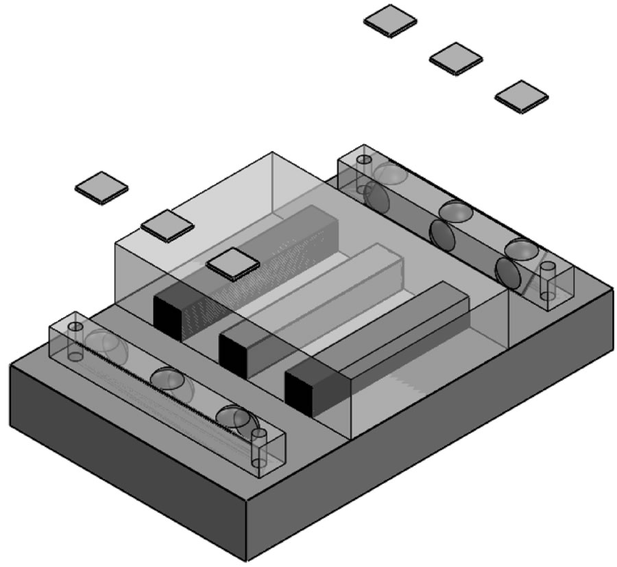
Embedded multimode waveguides in printed wiring boards can have several parallel channels utilizing one VIA, as shown in Figure 2(a). If one channel of a waveguide group is slightly longer than the other waveguides in the group, its coupling efficiency can be significantly less (1 - 6 dB) than its neighbors leading to that channel to exceed the overall link budget. A change in index of refraction from heating of the board or aging of the material would additionally impact the coupling efficiency [6]. If the index of the board changes by 0.01, the optical path length changes by 1 mm per 10 cm length resulting in a new modal structure that is coupled to the optical VIA changing the coupling efficiency appreciably on the order of 1 - 6 dB.
An optical electrical printed wiring board section is shown in Figure 2 to indicate how the VIA is located within the embedded waveguide layer. The optical VIA consists of a molded block of Polymethyl methacrylate (PMMA). The index of refraction, (n = 1.41), allows for a 45˚ total internal reflection mirror to turn the light 90˚. There are two 50 μm curvature lenses separated by an optical path length of 70 μm located at the entrance and
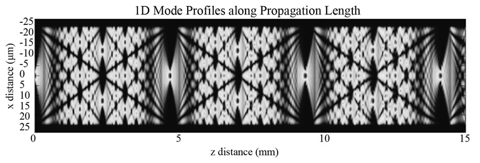
Figure 1. Repeating mode length.
 (a)
(a)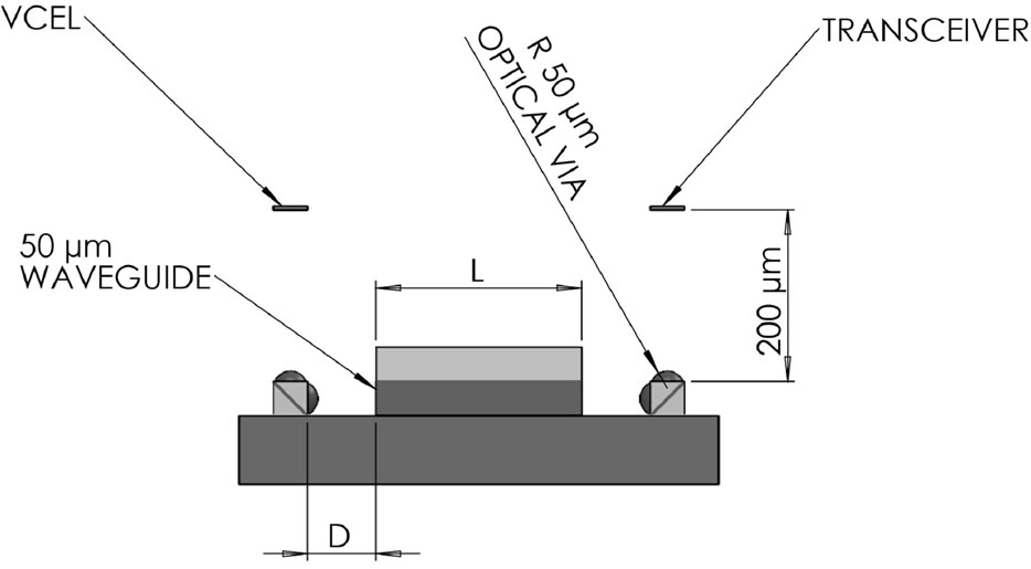 (b)
(b)
Figure 2. Optical VIA placement in waveguide layer. (a) Isometric View; (b) Front View.
exit of the optical channel. Approximating that the total internal reflection mirror is a perfect mirror, the overall effective focal length of the system is 76.5 μm.
To find the optical coupling loss of the VIA two separate simulations were performed. First, varying waveguide field outputs dependent upon the length of the waveguide were modeled using the beam propagation method [7-9]. Then, the efficiency through the VIA was modeled for each length of waveguide (L). This process was repeated for different waveguide end to VIA distance, D, ranging from 50 μm to 150 μm, which was chosen to reflect the dimensions of the milled waveguide trenches.
2. System Model Layout
The field distributions for each length of waveguides were found by modeling a 50 μm × 50 μm embedded step index square waveguide. The setup for the simulation is shown in Figure 3. The beam propagation method was used to find the field distribution for each length, L, of waveguide. This method is applicable because the field amplitude slowly varies in the propagation direction [10]. Simple transparent boundary conditions were used [11] because they are most suited for highly multimode problems [12]. An additional absorbing layer with a width of 12.5 μm was added to ensure field falloff of the model. The index of the core of the material is 1.52 and the cladding index is 1.50. These indices were chosen to match Dow Corning’s OE414x polymer waveguide material. The input of the simulation was a 5.6 μm single mode fiber. The numerical aperture of the fiber was 0.24 and illuminated the waveguide with 1 mW of light. This was chosen because it was assumed that the VCSEL or single mode fiber input shown in Figure 2 was mirrored onto the waveguide face. The field was first propagated 1 mm to ensure mode coupling losses were taken into account. The field output was sampled every 10 μm until the field had repeated itself as shown in Figure 1. A summary of the simulation parameters is given in Table 1.
Using the calculated field distribution outputs, the light was propagated through the VIA assembly using an angular spectrum propagator [13]. The angular spectrum representation in the frequency space is shown in Equation 1.
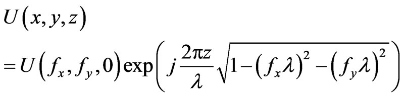 (1)
(1)
where 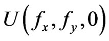 is the Fourier transformed input field calculated from the field distribution outputs, fx and fy are the spacial frequency components, λ is the free
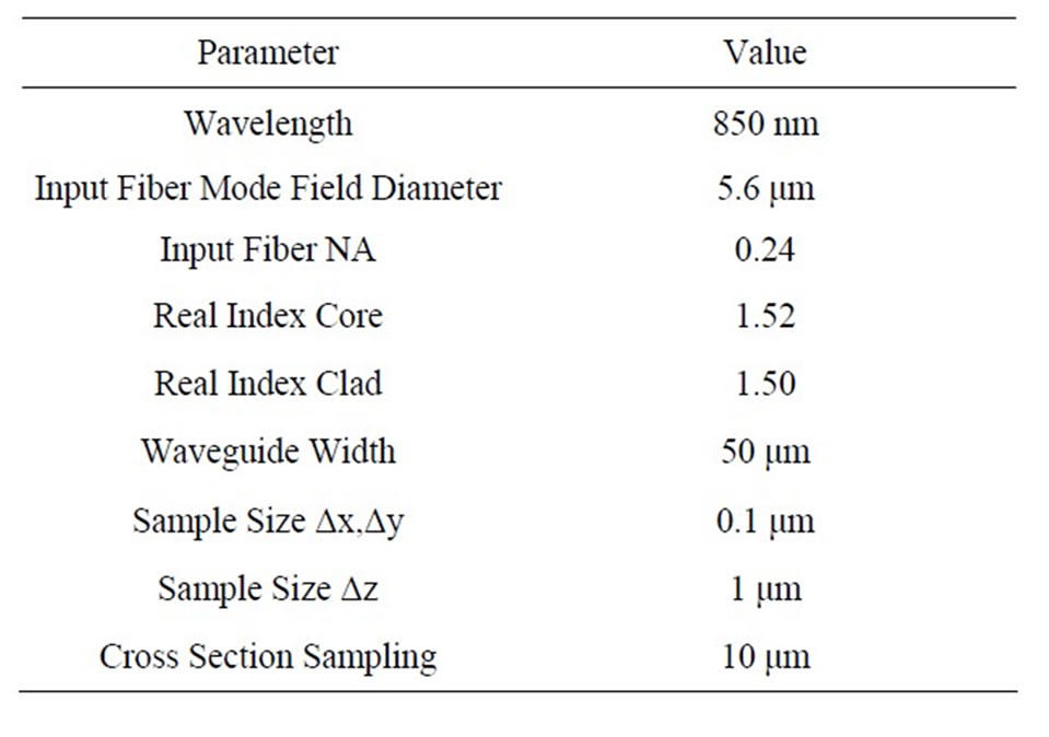
Table 1. Waveguide simulation parameter.
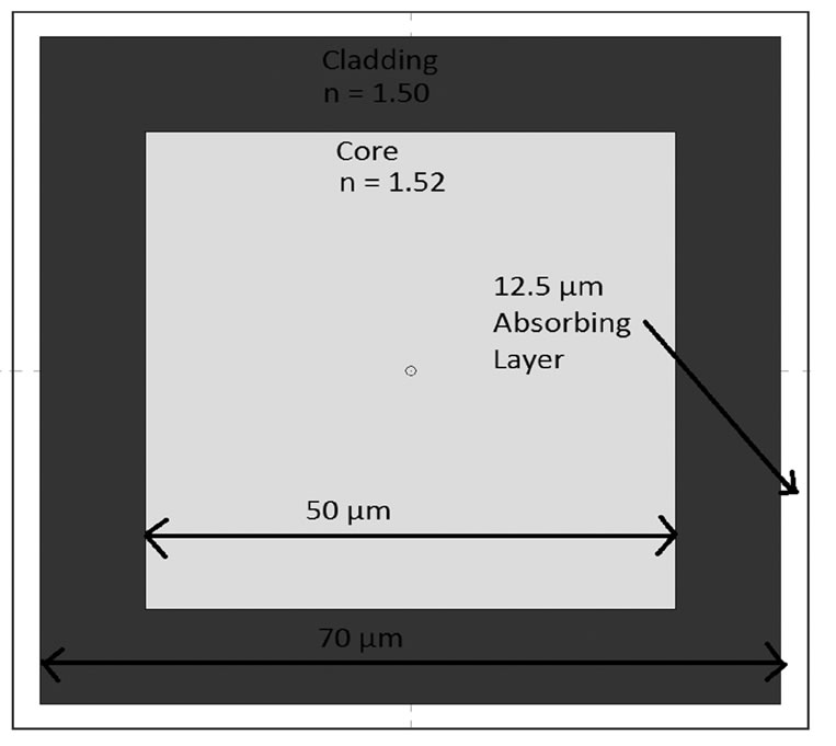
Figure 3. Buried waveguide setup for BPM simulation.
space wavelength, and z is the propagation distance. After propagation to the lens the angular spectrum becomes:
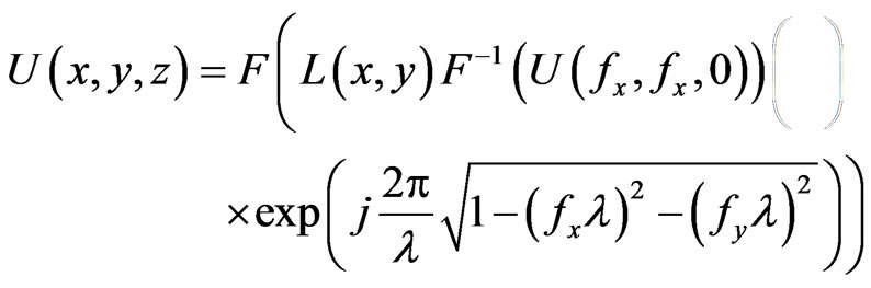 (2)
(2)
where F[…] designates the Fourier transform of a function. L(x,y) is the contribution of an aberration free lens defined by [14]:
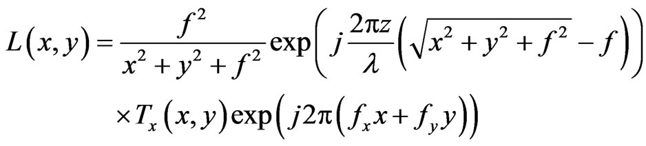 (3)
(3)
where Tx is the reflection coefficient at the lens boundary and f is the focus of the lens. The setup for determining the reflection coefficient of the lens is shown in Figure 4. In determining the reflection coefficient, it is assumed that all the light incident upon lens is parallel to the optical axis, or φ = 0, (paraxial assumption). This assumption is valid because the reflection coefficient, Ris roughly the same for small angles of φ, or 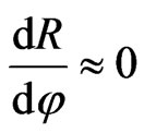 for small angles of phi.
The angle of incidence can then be simplified to:
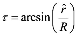 (4)
(4)
where r is the height of the incident parallel ray and R is the radius of the lens. To determine an paraxial transmission coefficient, it is also assumed that all the light hitting the VIA is randomly polarized.
The input field, the lens and output field must be sampled at:
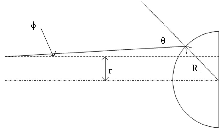
Figure 4. Setup for determining reflection coefficient, Tx.
 (5)
(5)
Which is twice as much as reported in [14] but is needed to satisfy Nyquist criterion. Where z is the overall optical path length. For most lens systems this criterion leads to unrealistic array sizes and run times, but in the case of microlenses such as the VIA this application is efficient [15].
All the field outputs generated from the beam propagation method were then put through the lens system of the optical VIA shown in Figure 5. In the optical system D is sampled as 21 different free space propagation portions of length between 50 and 150 μm in increments of 5 μm. The output field then encounters the first lens and travels 70 μm in an index of 1.41. Finally a third simulation was run propagating the field from the second lens interface 200 μm to the 50 μm square sensor. The power on the detector compared to the power from the waveguide output is defined as the system efficiency.
3. Results
Figure 6 shows two samples of how the coupling efficiency of the VIA assembly changes depending on the length of the waveguide. The attenuation of both waveguide to VIA distances shows significant differences in efficiency depending on the waveguide length, L, although there is a relativity small difference between the two lengths, D. To determine the optimal VIA placement distance three metrics were used to determine the optimal placement of the VIA, the highest average power, the lowest variance, and the worst-case scenario.
The first metric was obtaining the optimal waveguide to VIA distance based on the average power of the all the waveguide lengths. The attenuation of the distance the VIA is away from the waveguide end-face, D, distance is shown in Figure 7. The optimal placement for the VIA using this metric was 150 μm away from the waveguide. This result is interesting because using geometrical optics the optimal focal point appears at 123.9 μm. A possible reason for the difference may be the beam waist for each
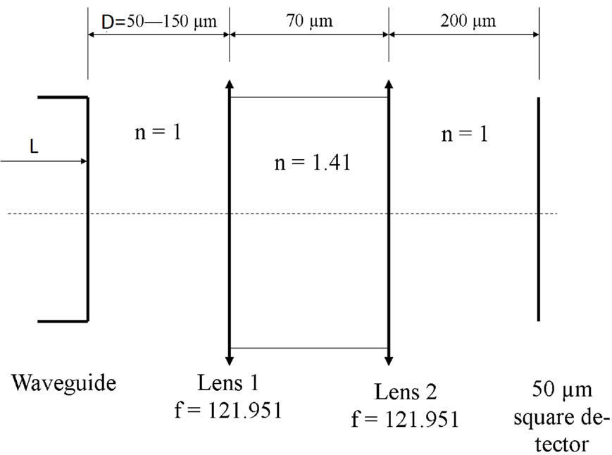
Figure 5. Optical setup the VIA propagating a field through the VIA.
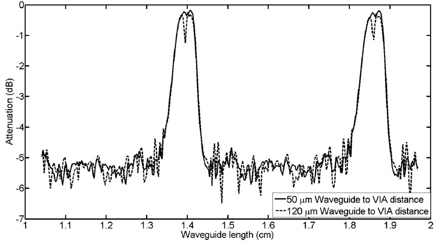
Figure 6. Attenuation of VIA assembly for two waveguide to VIA lengths.
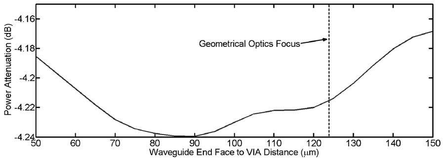
Figure 7. Average power of VIA assembly.
mode will be slightly different, resulting in a circle of least confusion and not a true focal point.
The second metric was the variance of the power in the VIA assembly. Minimizing the variance of the system also minimizes the amount of waveguide channels that are deemed out of tolerance. Figure 8 shows the variance depending on the waveguide to VIA distance. The optimal placement of the VIA using this metric is also 150 μm. This metric is in good agreement with the average power simulations.
The final metric found the lowest attenuation with the worst-case waveguide length distance, or the optimal distance using the worst-case scenario. This metric is important in minimizing the amount of waveguides that are deemed out of tolerance in a multichannel optical VIA. The results for the simulation are shown in Figure 9. The optimal distance with this metric is 60 μm with an
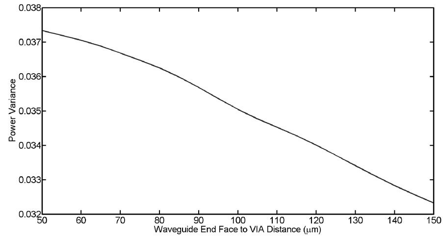
Figure 8. Variance in power of VIA assembly.
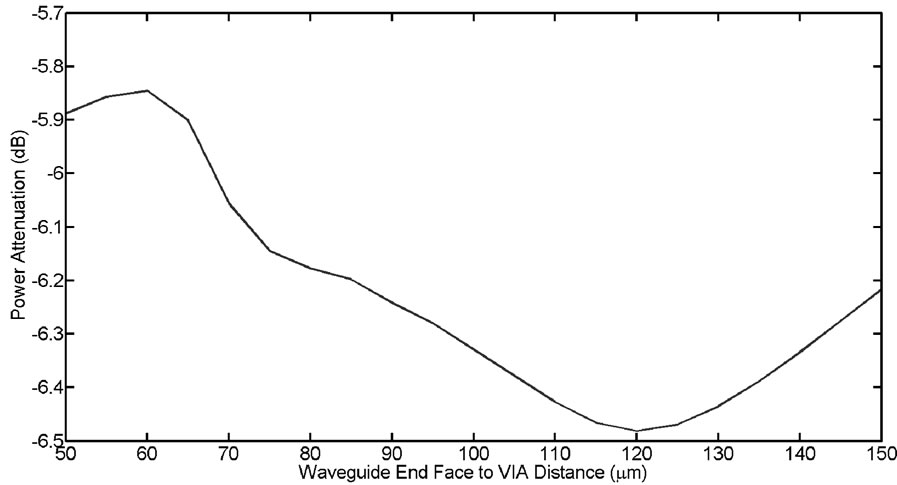
Figure 9. Worst case attenuation of VIA assembly.
attenuation of 5.85 dB.
4. Conclusion
To determine the optical loss in an optical VIA for embedded multimode waveguide applications, a single mode fiber input was propagated along a 20 mm waveguide to mimic field structures present at the output. The single mode input was launched into a 50 μm square multimode structure. Losses for the system ranged from 0.177 dB to 6.48 dB. For optimal VIA placement that, on average, couples effectively or has the smallest variation with respect to changes in the waveguide attenuation, the VIA placement should be just beyond geometrical optics optimal focal point at 150 μm away from the end of the waveguide. To have the least amount of coupling loss for all waveguide distances, the VIA should be placed before the geometrical optical optimal focal point at 60 μm away from the end of the waveguide. Using these metrics it is possible to blind pick and place a waveguide VIA so that the attenuation or variance of the waveguide channels of the VIA assembly is minimized.
5. Acknowledgments
This work was conducted by the HIOPTIMA group at Michigan Technological University and was supported by NAVAL Air Systems Command under Contract Number: N00421-090D-003. OE-4140 and OE-4141 are developmental materials produced by Dow Corning Corporation and are not commercially available. Commercial products are identified for reference only.
REFERENCES
- D. Huang, T. Sze, A. Landin, R. Lytel and H. Davidson, “Optical Interconnects: Out of the Box Forever?” IEEE Journal of Selected Topics in Quantum Electronics, Vol. 9, No. 2, 2003, pp. 614-623. http://dx.doi.org/10.1109/JSTQE.2003.812506
- C. Berger, M. A. Kossel, C. Menolfi, T. Morf, T. Toifl and M. L. Schmatz, “High-Density Optical Interconnects within Large-Scale Systems,” Photonics Fabrication Europe, International Society for Optics and Photonics, 2003, pp. 222-235.
- N. Savage, “Linking with light [high-speed optical interconnects],” IEEE Spectrum, Vol. 39, No. 8, 2002, pp. 32- 36. http://dx.doi.org/10.1109/MSPEC.2002.1021941
- A. Neyer, S. Kopetz, E. Rabe, W. Kang and S. Tombrink, “Electrical-Optical Circuit Board Using Polysiloxane Optical Waveguide Layer,” Proceedings of 55th Electronic Components and Technology Conference, Lake Buena Vista, 31 May-3 June 2005, pp. 246-250. http://dx.doi.org/10.1109/ECTC.2005.1441274
- L. B. Soldano and E. C. M. Pennings, “Optical MultiMode Interference Devices Based on Self-Imaging: Principles and Applications,” Journal of Lightwave Technology, Vol. 13, No. 4, 1995, pp. 615-627.
- B. W. Swatowski, C. T. Middlebrook, K. Walczak and M. C. Roggemann, “Optical Loss Characterization of Polymer Waveguides on Halogen and Halogen-Free fr-4 Substrates,” Proceedings of SPIE, Vol. 7944, 2011, Article ID: 794409. http://dx.doi.org/10.1117/12.866081
- M. D. Feit and J. J. A. Fleck, “Computation of Mode Properties in Optical Fiber Waveguides by a Propagating Beam Method,” Applied Optics, Vol. 19, No. 7, 1980, pp. 1154-1164. http://dx.doi.org/10.1364/AO.19.001154
- W. Huang, C. Xu, S.-T. Chu and S. Chaudhuri, “The Finite-Difference Vector Beam Propagation Method: Analysis and Assessment,” Journal of Lightwave Technology, Vol. 10, No. 3, 1992, pp. 295-305. http://dx.doi.org/10.1109/50.124490
- K. Okamoto, “Fundamentals of Optical Waveguides,” Elsevier, 2006. http://dx.doi.org/10.1007/BF00619865
- L. Thylén, “The Beam Propagation Method: An Analysis of Its Applicability,” Optical and Quantum Electronics, Vol. 15, No. 5, 1983, pp. 433-439.
- D. Yevick, “A Guide to Electric Field Propagation Techniques for Guided-Wave Optics,” Optical and Quantum Electronics, Vol. 26, No. 3, 1994, pp. S185-S197.
- R. D. Grounp, “BeamPROP Maunal Revision C,” Rsoft Design Group, Inc., Ossinging, 2011.
- J. W. Goodman, “Introduction to Fourier Optics,” 3rd Edition, Roberts & Company Publishers, Englewood, 2004.
- S. Odate, C. Koike, H. Toba, T. Koike, A. Sugaya, K. Sugisaki, K. Otaki and K. Uchikawa, “Angular Spectrum Calculations for Arbitrary Focal Length with a Scaled Convolution,” Optics Express, Vol. 19, No. 5, 2011, pp. 14268-14276. http://dx.doi.org/10.1364/OE.19.014268
- N. Lindlein, “Simulation of Micro-Optical Systems Including Microlens Arrays,” Journal of Optics A Pure and Applied Optics, Vol. 4, No. 4, 2002, p. S1.