Optics and Photonics Journal
Vol. 3 No. 2A (2013) , Article ID: 33337 , 7 pages DOI:10.4236/opj.2013.32A002
Design, Simulation & Optimization of 2D Photonic Crystal Power Splitter
1Photonic Networks Engineering (MAPNET), Scuola Superiore Sant’Anna, Pisa, Italy
2Department of Electrical & Electronic Engineering, University of Information Technology & Science, Dhaka, Bangladesh
3Department of Electronics & Telecommunication Engineering, Rajshahi University of Engineering & Technology, Rajshahi, Bangladesh
4Department of Physics, Bangladesh University of Engineering and Technology, Dhaka, Bangladesh
Email: *rajib.ahmed.apece@gmail.com, masrufsamgroup11@gmail.com, rifat.ete07@gmail.com, abdulahadbbaria@hotmail.com
Copyright © 2013 Rajib Ahmed et al. This is an open access article distributed under the Creative Commons Attribution License, which permits unrestricted use, distribution, and reproduction in any medium, provided the original work is properly cited.
Received November 18, 2012; revised February 14, 2013; accepted March 22, 2013
Keywords: Power Splitter; Photonic Crystals; Finite Difference Time Domain; PCLDMMI; MLDPCW
ABSTRACT
A very compact (80 - 100 μm2) integrated power splitting devices with two outputs (1 × 2), four outputs (1 × 4) and six outputs (1 × 6) channel has been designed, simulated and optimized for Telecommunication purpose with T-Junction, Y-Junction, PC line defect waveguides integrated with multimode interference block (PCLD-MMI) and multiple line defect PC waveguides (MLDPCW) configurations. The optical modeling of these proposed structures was investigated by finite difference time domain (FDTD) simulation. With the optimization of the parameters (Hole Radius, R = 0.128 µm, Input Diameter, D = 1.02 µm, Input wavelength, λ = 1.55 µm, Substrate Reflective Index, nsub = Si(1.52), Photonic Crystal Material, npcs = InAs(3.45), and Rectangular crystal structure), 1 × 2 for Y-Junction (100%), 1 × 4 for T-Junction (92.8%) and 1 × 6 configuration for MLDPCW (81%) show maximum power transmission.
1. Introduction
In the recent years, a lot of research has been focused on developing micro and nano photonic devices by using Photonic Crystals (PCs). Photonic Crystals (PCs) are artificial structure in which the periodic variation of dielectric constant is used to control the flow of light. PCs may be 1D, 2D & 3D crystal structure. Unlike electronic crystals (which are natural structure) that control the flow of electron by periodic variation of electron potential and follow Schrödinger equation, PCs follow Maxwell’s equation [1].
Nowadays, from the idea of controlling light by means of Photonic Crystal (PC) has led to many proposals and implementations for novel devices including different types of power splitters has generated wide interests in the communication field. This is possible only for periodic variation of the refractive index causes photonic band gap and artificially introduced defects to divide the input power equally into the output channels without significant reflection or radiation losses with compact in size. The traditional limitation on power splitter based optical fiber on is on transmission loss can be minimized by the photons splitter as optimal one [2]. It has many advantages such as low loss, good uniformity, insensitive to operation wavelength, polarization, large bandwidth, simple fabrication technique, larger tolerance, minimized structure, temperature and other environmental factors.
Researchers have theoretically investigated photonic crystal with an array of dielectric rods in air. Based on this concept the T-junction, Y-junction and MMI effects have already been extensively studied [3,4]. Unfortunately, the “rod in air” approach does not provide sufficient vertical confinement and is difficult to implement for most practically useful device implementations in the optical regime. A slab waveguide structure consists of air holes etched into a dielectric medium such as silicon, GaAs/AlGaAs hetero structure or a semiconductor membrane which remedies this problem and allows waveguides with tolerable losses [5,6]. This Multimode leads to mode-mixing problem at the intersection of the PCW which creates a mismatch between input and output fields and introduces large reflections at the interface.
In this paper, new power splitting techniques using 2-D and 2-D slab PC line defect waveguides are investigated. In order to achieve this, initially we investigated (a) T-junction structure for 1 × 2 and 1 × 4 applications. Then, (b) Y-junction with 1 × 2, 1 × 4, 1 × 6 structures are also invested. In this scheme, we have improved the power transmission and output spectrum in 1 × 2 application which is better than published result where as in 1 × 4 and 1 × 6 applications the power transmission and output spectrum is not good enough for practical application point of view. So, in order to improve the powertransmission and output spectrum we have investigated two new designs where one is (c) PC line defect waveguides are integrated with a multimode interference (MMI) block and multiple line defect PC waveguides (MLPCW) for 1 × 2, 1 × 4, 1 × 6 power splitting applications. In MLPCW scheme, we have investigated the three versions which are a combination of three, five and seven line defect waveguides. These two structures are more compact than the previous design but relatively broad spectrum. Among those structures Y-junction based 1 × 2 power splitter was found best with 100% transmission and equally splitting. Optical modeling is used to demonstrate that the power is equally divided at each output channel with a relatively broad spectrum. Moreover, FDTD simulation method is used to overcome some of the difficulties of previous works (i.e. mode mismatch, bandwidth and bending region transmission) and challenges. The structure can be applied to communication systems and also be integrated with other PC based devices.
2. Layout Design and Simulation
We have taken SiO2 as a wafer material (reflective index 1.447) with dimension—length-30 μm and width-48 μm, Gaussian modulated continuous wave as an input signal with wavelength 1.55 μm. Both transverse and injection type of the input is Modal. The input signal used in the simulation expressed as,
 (1)
(1)
where, A is the field amplitude and  is the transverse field location at the incident field location zinc. The initial offset θi is the phase difference between points in the incidence plane. This offset can be adjusted to define the direction of the incident field [1]. The planar PC structure is simulated on a silicon-on-insulator substrate with a Si slab of thickness t = 220 nm separated from the Si substrate by 1 μm silica layer. The holes are placed in a triangular lattice and have a diameter d = 0.588Λ, where “Λ” is the lattice constant.
The propagation of light in the waveguides is simulated by 2D Finite-difference time-domain (FDTD) method using a standard simulator. FDTD is a time-domain numerical method used for modeling the propagation of electromagnetic waves in optical media, which is based on the discretization of Maxwell’s equations in differential form in free space. Time domain methods have been found to be very accurate in simulating the propagation dynamics of signals in periodic dielectric media [7].We simulate for TE mode, actual Mesh used- 0.075 μm (delta X) × 0.075 μm (delta Z) with number of mesh cells 400 (X) and 650 (Z). For result finalization the simulation has been done for 4000 time steps. The Anisotropic Perfectly Matched Layer (APML) boundary condition is used. PC line defect waveguides (LDWs) integrated with MMI block for power splitting has potential to transmit power from the input to the output without any changes of the PC dielectric hole size. It has a large optical bandwidth as compared to existing power splitter. In proposing design there are no 120˚ junctions or 60˚ bends. As a consequence the single mode operation will not be suffered. The entire structure will be formed by a triangular lattice of dielectric holes so the vertical confinement will be better as compared to the triangular lattice of dielectric rod structure. An account of having all these advantages the entire structure can be considered as a 2-D slab PC configuration. Therefore, the application of power splitter by using PCLDWs integrated with MMI is attractive.
It is known that the typical Y-junction structure has poor transmission without any structural tuning at the bends and input and output ports. In addition to that the performance of the Y-junction can be improved by tuning and displacing the holes at 120˚ junction and also by bending the output ports but still difficulties exist which cannot be easily addressed for practical application. These difficulties arise from the mode-mismatch at 120˚ junction and the bending loss from the output ports. It is conspicuous from a number of the researcher’s work that Y-junction based power splitter itself identifies some problems in its own design. Here a unique design is proposed which will not be having any disturbances like 120˚ junction and bending loss. 2-D PC multiple line defect waveguides based power splitter is that proposed design which will be capable of addressing the issues of Y-junction based power splitter as mention before. PC multiple line defect waveguides power splitter minimizes the multimode mode problem occurred in the existing design. Therefore, this proposed scheme transmits more power as compared to the existing design. So, PC multiple line defect waveguides based power splitter should be investigated.
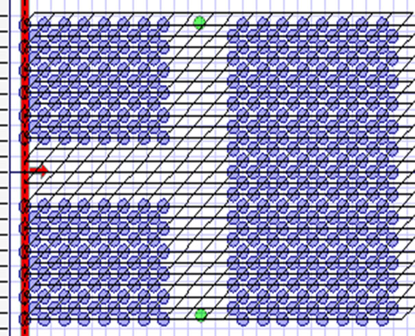
The real motivation behind using PC waveguides over conventional dielectric waveguides for optical intercomnects includes better routing capabilities with lower transmission, bending loss, coupling loss, reduced cross talk and larger design flexibility provided by the PC environment, monolithic integration with other on-chip photonic component like a PC based laser or photo-detector. A schematic representation of an optical signal distribution layer using PC based waveguides (Line defect waveguides) integrated with MMI block is shown in Figure 1. The architecture of output optical signal consists of four PC line defect waveguides (LDWs) which is integrated with MMI block. The optical signal is equally divided at the each output channel, shown in Figure 2.
 (A1)
(A1)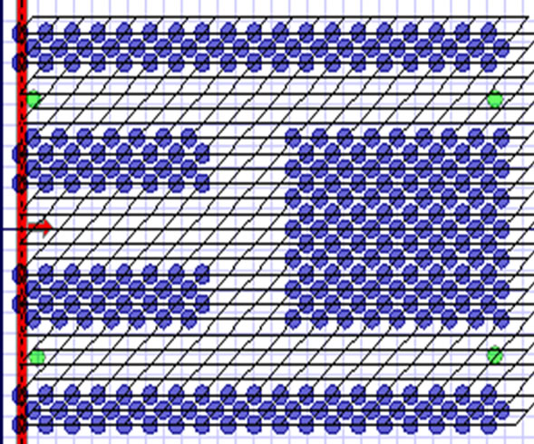 (A2)
(A2)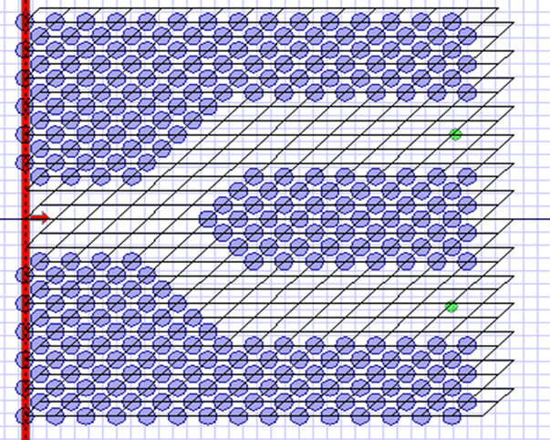 (B1)
(B1)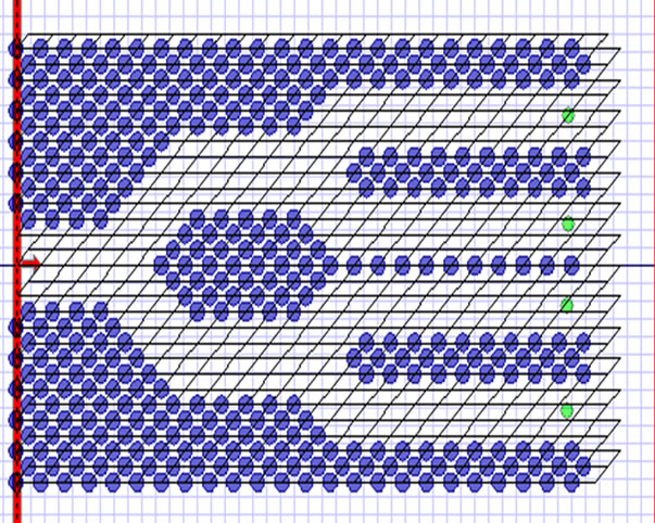 (B2)
(B2)  (C1)
(C1)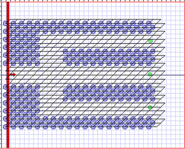 (C2)
(C2)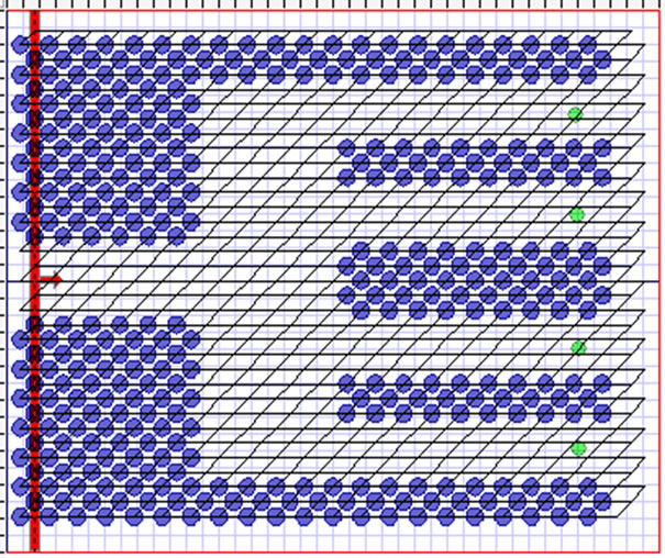 (C3)
(C3)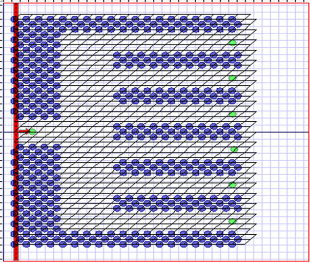 (C4)
(C4) (D1)
(D1)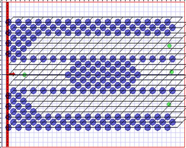 (D2)
(D2)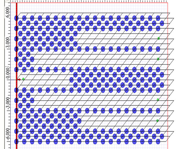 (D3)
(D3)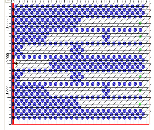 (D4)
(D4)
Figure 1. Layout design of 1 × 2 T-Junction (A1), 1 × 4 T-Junction (A2), 1 × 2 Y-Junction (B1), 1 × 4 Y-Junction (B2), 1 × 2 PCLD-MMI (C1), 1 × 3 PCLD-MMI (C2), 1 × 4 PCLD-MMI (C3), 1 × 6 PCLD-MMI (C4), 1 × 2 MLDPCW (D1), 1 × 3 MLDPCW (D2), 1 × 4 MLDPCW. (D3), 1 × 6 MLDPCW (D4).
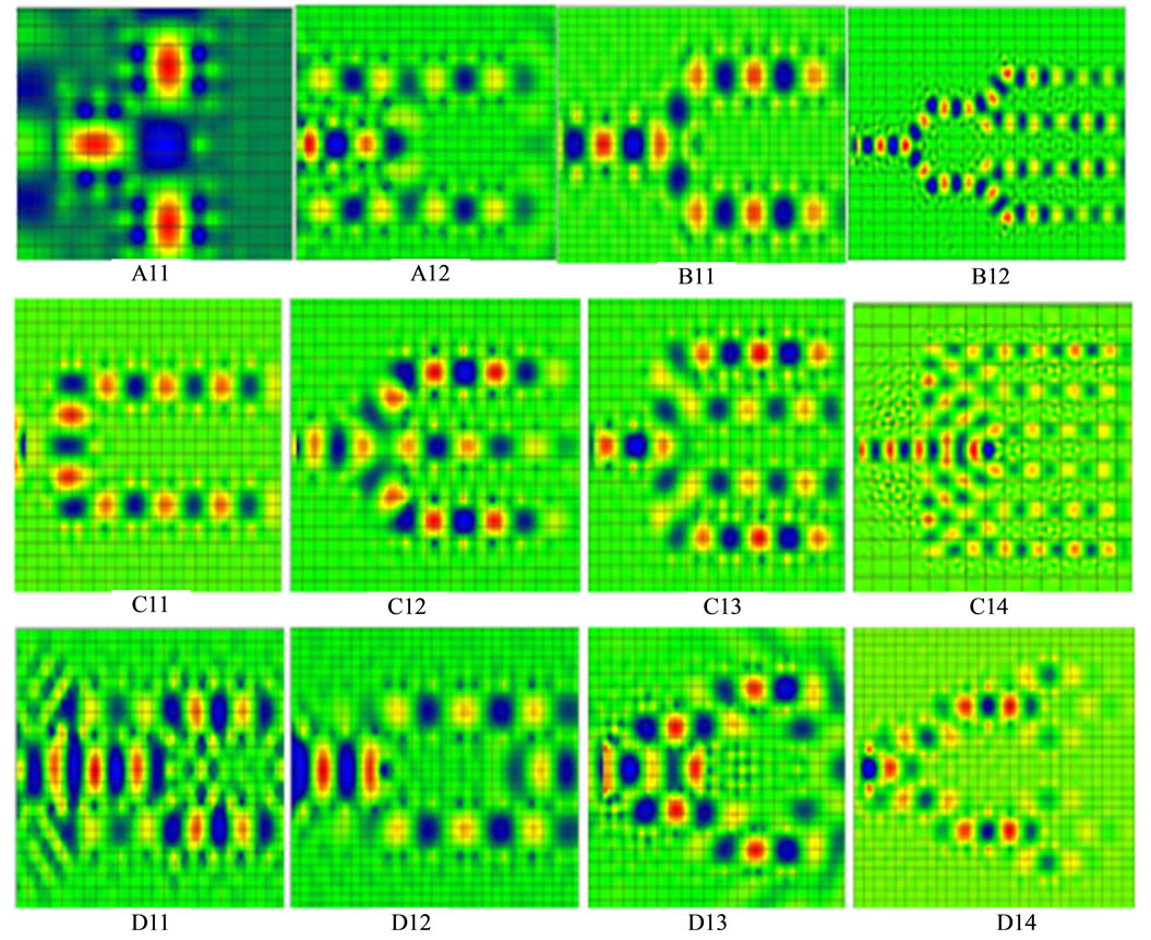
Figure 2. Simulation result of 1 × 2 T-Junction (A11), 1 × 4 T-Junction (A12), 1 × 2 Y-Junction (B11), 1 × 4 Y-Junction (B12), 1 × 2 PCLD-MMI (C11), 1 × 3 PCLD-MMI (C12), 1 × 4 PCLD-MMI (C13), 1 × 6 PCLD-MMI (C14), 1 × 2 MLDPCW (D11), 1 × 3 MLDPCW (D12), 1 × 4 MLDPCW (D13), 1 × 6 MLDPCW (D14).
3. Results Analysis
We try to optimize the parameters of the splitter. For the variation of the input port diameter (0.15 - 1.4 μm), optimize value found for 1.02 μm (keeping fixed the Lattice constant, Λ = 1 μm and Hole Radius, R = 0.128 μm). With an optimum diameter (D = 1. 02 μm), the hole radius of the photonic crystal (R) are varied (0.1 - 0.15) to get the optimize value of hole radius, R = 0.128 μm (keeping fixed the Lattice constant, Λ = 0.435 μm). Similarly, from the variation of the input wavelength, λ (1.5 - 1.6 μm) the optimize value found λ1 = 1.55 μm (TE Mode) and λ2 = 1.6 μm (TM Mode). Moreover, we take Air (n = 1), Glass /Si (n = 1.52), GaAs (3.40), InAs (3.45), InGaAs (3.72) as a wafer and Photonic Crystal (PC) material and found Si as wafer and GaAs (3.40) as a optimize PC material. Similarly, with Rectangular, Hexagonal, Face-centered cubic (FCC) and Body-centered cubic (BCC), optimized structure is found in Rectangular Crystal. The decision of optimization is based maximum power transmission on the output ports.
We have investigated the transmission of the structures using a 2D FDTD method with perfectly matched layer(PML) boundary condition. The output transmitted power of 1 × 2 T-Junction is monitored at two points on the 90˚ bend output waveguides; one at the output of channel 1 (CH1) and the other at the output of channel 2 (CH2) is indicated in Figure 1. The output spectrum indicates that a maximum of 46.4% of the input power through each channel and total 92.8% of input power is transmitted. Similarly, total 83% of input power is transmitted for 1 × 4 T-Junction. In this 1 × 2 case, output ports are 90˚ bands to the inputs for single time but two times for 1 × 4 T-junctions and thus power reduces to 83% from 92.8%.
The improved structure of T-junction is Y-junction in which total 100% and 86% are transmitted for 1 × 2 and 1 × 4 Y-junctions splitter due to lower bends (60˚) of output ports. The structure of this Y-junction is formed by the intersection of three PCW at 120˚. The output channels have an additional 60˚ bend which is parallel to the input channel as shown in Figure 1. Due to 120˚ junction and 60˚ bend; single mode operation might suffer which can cause the reflection and large transmission loss. To overcome these difficulties the junction and bend must be carefully designed. The better transmission can be achieved by the modified Y branch structure in which the 60˚ bends are modified by displacing or removing one or more holes and changing their shapes in the bend.
The PC-based Y-junction power splitter has problems with mode mismatch and bending loss which excites the higher order modes. So in order to obtain an acceptable output transmission, the bending region needs to be carefully optimized which adds difficulties in design and fabrication. To minimize mode mismatch and bending loss, many researchers have investigated theoretically on an array of dielectric rods in air.
To avoid some of the above difficulties and challenges, in this thesis we have investigated a novel idea for a 1 × 4 power splitting technique which is a 2D photonic crystal triangular lattice of dielectric air holes line defect waveguides integrated with an MMI block. Moreover, the proposed power splitter structure overcomes the mode matching phenomena, poor transmittance of Yjunction structure and the limited bandwidth and is easier to fabricate as compared to a Y-junction structure and MMI affect dielectric rod structure. The structure can be applied to optical communication systems and also be integrated with other PC-based devices.
Here, Figure 3 shows the maximum power transmission with respect to wavelength. Moreover, Table 1, Table 2 and Table 3 shows the comparison between different 1 × 2, 1 × 4 and 1 × 6 power splitters respectively.
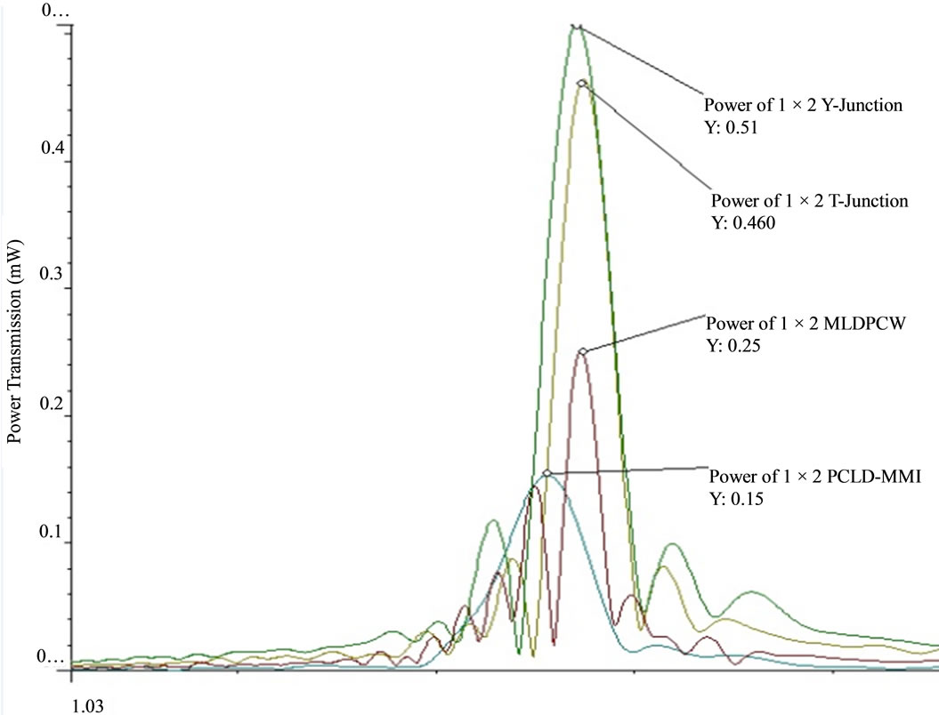
Figure 3. Power transmission mw, (Y-axis) vs Wavelength μm, (X-axis) for 1 × 2 photonic power splitters (per channel).
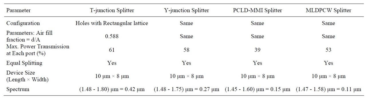
Table 1. Comparison of different 1 × 2 power splitters.
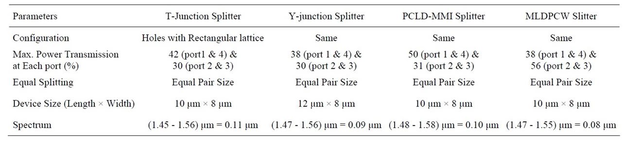
Table 2. Comparison of different 1 × 4 power splitters.
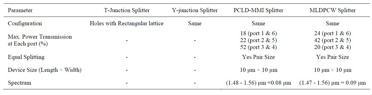
Table 3. Comparison of various 1 × 6 power splitters.
4. Conclusion
T-junction, Y-Junction, PCLD-MMI Splitters and PCLDW splitters in different lattice configurations (like Rectangular, Hexagonal, FCC and BCC structures) with TE and TM mode have been designed, simulated with FDTD method. The performance of each structure was characterized and compared with each other by maximum power transmission. It has shown the different type splitter to have relatively higher transmission efficiency in contrast with others. Finally, with optimized parameters the output power is different and their comparison with different configurations has been done. Based on these structures optimizations higher efficiency power splitters were designed which can be used in networking, modulation, transmission, switching etc. applications.
5. Acknowledgements
All thanks due especially to our parents for their prayer and inspiration, which has helped us in becoming what we are today.
REFERENCES
- J. D. Joannopoulos, R. D. Meade and J. N. Winn, “Photonic Crystals: Molding the Flow of Light,” Princeton University Press, Princeton, 1999.
- Rajat Dey, “Optical Power Splitting Techniques Using Photonic Crystal Line Defect Waveguides,” Ph.D Thesis, The University of Western Ontario, London, Canada, 2011.
- T. Yu, H. Zhou, J. Yang, X. Jiang and M. Wang, “Ultra Compact Multi-Way Beam Splitters Using Multiple Coupled Photonic Crystal Waveguides,” Journal of Physics D: Applied Physics Vol. 41, No. 9, 2008, pp. 1-5. doi:10.1088/0022-3727/41/9/095101
- S. Fan, S. G. Johnson, J. D. Joannopoulos, C. Manolatou and H. A. Haus, “Waveguide Branches in Photonic Crystals,” Journal of the Optical Society of America B, Vol. 18, No. 2, 2001, pp. 162-165. doi:10.1364/JOSAB.18.000162
- E. Chow, S. Y. Lin, S. G. Johnson and P. R. Villeneuve, “Three-Dimensional Control of Light in Two-Dimensional Photonic Crystal Slab,” Nature, Vol. 407, No. 6807, 2000, pp. 983-986. doi:10.1038/35039583
- M. Notomi, A. Shinya, K. Yamada, J. Takahashi, “Single Mode Transmission within Photonic Bandgap of WidthVaried Single-Line-Defect Photonic Crystal Waveguides on SOI Substrates,” Electronics Letters, Vol. 37, No. 5, 2001, p. 293. doi:10.1049/el:20010195
- A. Taflove, “Computational Electrodynamics: The Finite-Difference Time-Domain Method,” Artech House, Boston, 1995.
NOTES
*Corresponding author.