Optics and Photonics Journal
Vol.2 No.3A(2012), Article ID:23300,4 pages DOI:10.4236/opj.2012.223031
Opal-Based Photonic Crystal Heterostructures
1CNR-IFN, CSMFO Laboratory, Via alla Cascata, Trento, Italy
2Dip. di Fisica, Università degli Studi di Trento, Via Sommarive, Trento, Italy
3Centro Fermi, Piazza del Viminale, Roma, Italy
4MDF Laboratory, IFAC-CNR, Via Madonna del Piano, Sesto Fiorentino, Italy
Email: *chiappini@science.unitn.it
Received June 22, 2012; revised July 23, 2012; accepted August 7, 2012
Keywords: Sol-Gel; Colloidal Crystals; Optical Properties; Heterostructures
ABSTRACT
The fabrication of photonic crystal heterostructures is important for the applications in the fields of integrated photonic crystal chips and multi-frequency optical Bragg filters or mirrors; here we report on the fabrication and characterization of opal-based photonic crystal heterostructures. These heterostructures are created by using multilayer deposition of silica and polystyrene spheres. In the specific the fabricated structures involved both different lattice constant and dielectric function. Scanning electron microscopy (SEM) and VIS-NIR transmittance and reflectance spectroscopy are used to characterize the systems. The SEM images show good ordering of the two-layer colloidal crystals constituting the heterostructures. The transmittance and reflectance spectra measured from the (111) plane of the heterostructure show that the composite colloidal photonic crystals have double photonic stop bands that matches the stop bands of the individual photonic crystals. This behaviour can be seen as a superposition of the properties of each individual layer.
1. Introduction
Photonic crystals have attracted great interests since the pioneering works of Yablonovitch and John [1,2]. These materials have the feature of the photonic bandgap (PBG) that forbids the propagation of the light in a particular range of frequencies through the structure. This property is due to the periodic variation of the refractive index of the crystals in one, two or three dimensions [3-5]. They can be used in several applications, such as optical switches [6], physical [7,8], chemical [9] and biological sensors [10,11] and low threshold lasers [12]. The research is focused on the fabrication of three dimensional photonic crystals (3D PC) because they offer the highest degree of light control.
Although top-down methods such as nanolithography, holography and direct laser writing can successfully design 3D PC, the high cost and the complex process have led to the development of efficient bottom-up techniques based on the colloidal crystals consisting of highly organized monodispersed colloidal particles [13-16]. It has been demonstrated from a theoretical point of view [17], as well as through experimental results [18], that these nanoparticles self-assemble in a face-centered cubic structure with the (111) plane parallel to the underlying substrates. Moreover these systems show opalescent colours due to the Bragg reflections by the lattice planes defined by the nanoparticles. In the specific the photonic band gap of these materials depends mainly on the lattice constant parameter, which is determined by the size of the constituting colloidal spheres and by the dielectric constant. Opal-based heterostructures (HTs) have attracted considerable attention from both the scientific and engineering points of view [19-21]. In the specific these systems were first introduced and investigated theoretically by Stefanou et al. [22]. From a structural point of view optical HTs are based on multiple layers of opal films with spheres of different lattice constant, different dielectric constant or both. It has been proved that these systems possess many attractive features, such as multistop band [23] and extended photonic band gap [24], which make these types of structures suitable for wide applications in manufacturing integrated photonic crystal chips, such as broadband reflective mirrors and/or multifrequency optical Bragg filters.
From a technological point of view several deposition techniques have been used for the fabrication of two-layer opal films structure such as the Langmuir Blodgett (LB) technique [25], convective self-assembly method [26,27] and more recently spin coating deposition method [28].
In this paper we report on the synthesis of monosize silica and polystyrene particles of different dimensions and we describe a suitable deposition protocol based on convective assembly that permits to grow on a silica opal different polystyrene (PS) colloidal crystals. Morphological and optical assessment of the systems realized is discussed.
2. Experimental
2.1. Synthesis of SiO2 and PS Nanoparticles
Silica nanoparticles (NPs) are prepared following the Stober method [13,29]. In particular tetraethylorthosilicate (TEOS), ethanol, concentrated ammonia and distilled water are used as reagents. Two mother solutions are prepared, containing TEOS-ethanol and ammoniawater-ethanol respectively, and then they are quickly combined in a reaction vessel. The mixture is stirred for 24 h with a magnetic stirrer. Subsequently, the silica suspensions are centrifuged at 3000 rpm for 30 min and washed with water. The centrifuging/washing procedure is repeated six times and finally the particles are dried at 50˚C overnight. Latex spheres are synthesized according to a single-stage polymerization process based on formation and growth of polymeric nuclei dispersed in an emulsion constituted by water, styrene, potassium persulfate (KPS) and sodium dodecyl sulfate (SdS) [30,31].
Briefly, the polymerization is carried out in a 500 ml glass reactor equipped with a stirrer, a reflux condenser and a heating jacket. All chemicals are used as received but styrene monomer, which is washed with NaOH and water to remove the polymerization inhibitor. The standard procedure is as follows: 245 ml of water, a suitable amount of sodium dodecyl sulphate dissolved in 13.6 ml of water and 27.2 ml of styrene monomer are premixed in the reactor at the temperature of 80˚C for 2 min and at a stirring speed of 300 rpm. To start the polymerization, an amount equal to 0.952 g of KPS dissolved in 13.6 mL of water is injected in the solution. After 4 h the polymerization is completed and after cooling down the colloidal solution is purified by repeated centrifugation/redispersion cycles.
2.2. Fabrication of Colloidal Crystal Films
The formation of direct colloidal crystals is obtained by vertical deposition (convective deposition method), which is based on the evaporation at 45˚C of the liquid (water) forcing the nanospheres to arrange in the meniscus formed between a vertical substrate, the suspension and air [13, 32]. In the specific the formation of the colloidal crystal films is achieved using silica nanoparticles about 320 nm in diameter and PS spheres of about 230 nm and 350 nm.
The morphology and structural properties of the heterostructures are characterized by scanning electronic microscopy (SEM) (JEOL6700). All the samples studied are not metalized. Optical properties are obtained by measuring reflection spectra using miniature fiber optic spectrometer with a 2 nm resolution, the incident light is perpendicular to the (111) plane of the colloidal crystal. Transmittance measurements are performed using a double beam spectrophotometer in the VIS-NIR range. An UV-Ozone cleaner is used in order to clean glass substrate for the deposition of the colloidal crystals and for the hydrophylization of the silica opal.
3. Results and Discussion
3.1. SiO2 and PS Colloidal Crystals
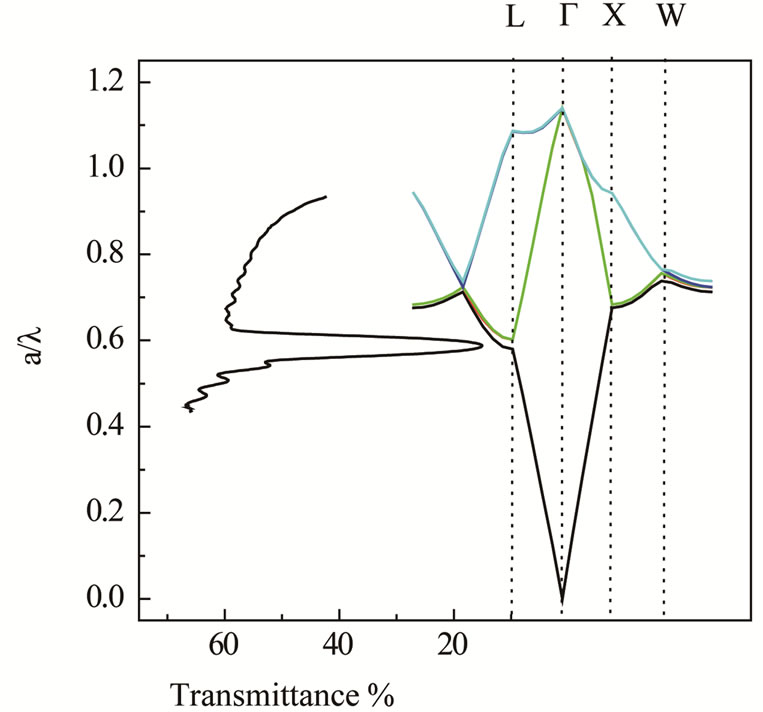
As a first step silica and polystyrene colloidal crystal films are deposited onto a glass slide by the vertical deposition method. In Figures 1(a) and (b) are reported the transmittance spectra of single colloidal crystal systems of PS and SiO2 and their photonic band structures obtained using the plane wave expansion method (MIT Photonic-Bands package) developed by Steven G. John-
 (a)
(a)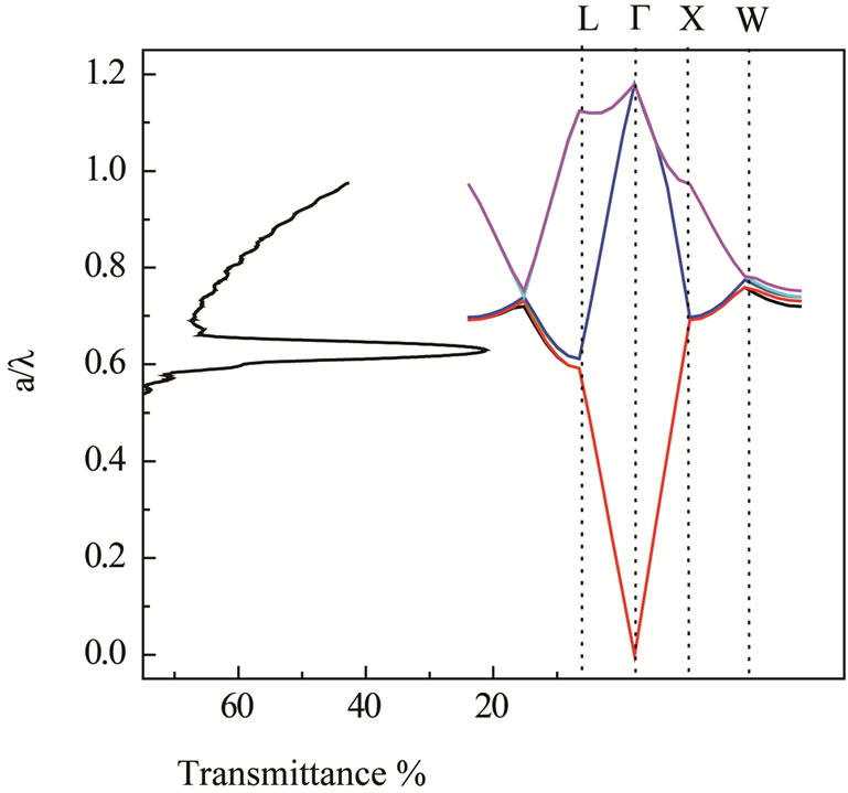 (b)
(b)
Figure 1. Photonic band structure of an fcc photonic crystal in the Γ-L direction and transmittance spectrum of (a) PS colloidal crystal and (b) SiO2 opal.
son [33]. From Figure 1(a) it is possible to observe a good agreement between experimental and theoretical results about the position of the pseudo band gap. In Figure 1(a) is also possible to notice the presence of a minimum in the transmittance spectrum at about 550 nm that arises due to the Bragg diffraction from the (111) planes of ordered structures. This minimum corresponds to the opening of a pseudo gap at about a/λ ~ 0.6 in the calculated Γ-L band diagram, where “a” is the lattice constant. Similarly for the case of the opal constituted by SiO2 NPs, reported in Figure 1(b), it is possible to observe the presence of an intense diffraction peak at about 700 nm in agreement with the position of the calculated pseudo gap along the Γ-L direction.
The position in term of wavelength of the pseudo band gap, at normal incidence, can be expressed by a modified Bragg’s Law [16]:
 (1)
(1)
where d111 = 0.816·D is the interplanar spacing of the (111) planes and D corresponds to the diameter of the nanoparticles; the neff is the effective refractive index that can be considered as follows [13]:
 (2)
(2)
where nspheres corresponds to the refractive index of the NPs used, nmedium is assumed equal to 1 and f is the filling factor that for a face cubic centred structure is 74%.
3.2. Characterization of the Heterostructures
The formation of the heterostructures occurs depositing on the SiO2 NPs colloidal film (bottom layer), opal structures of PS (top layer) that present different dimension in size; here two different type of HT systems will be discussed:
(i)1) 350 nm PS NPs on 320 nm SiO2 NPs (HT_350-PS/ 320-SiO2);
(ii)2) 230 nm PS NPs on 320 nm SiO2 NPs (HT_230-PS/ 320-SiO2)
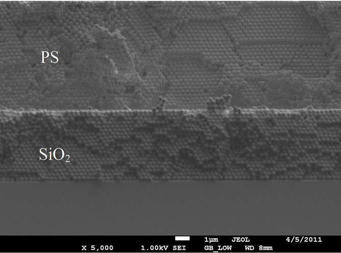
For both the structures an ozone treatment has been carried out in order to increase the wettability of the bottom layer and assure the adhesion of the second one. In Figure 2 is reported a typical SEM image relative to the cross section of a heterostructure (HT_350-PS/320-SiO2). Analyzing Figure 2 we can notice that the growth of the two photonic layers occurs and a good ordering of the structures realized is evident. This is confirmed from Figure 2(a) where the presence of the hexagonal arrangement for both the structures (bottom and top layer) can be clearly seen.
Moreover from Figure 2(b) we can observe a large ordered area of the top layer of the PS NPs, indicating the good quality of the structure obtained.
In Figure 3 are reported transmission and reflectance
 (a)
(a) (b)
(b)
Figure 2. (a) SEM image of cross section of a cleaved edge of a heterostructure constituted by silica (320 nm) and polystyrene (350 nm) NPs; (b) top view of the HT_350-PS/ 320-SiO2 where large domains of the top layer are present.
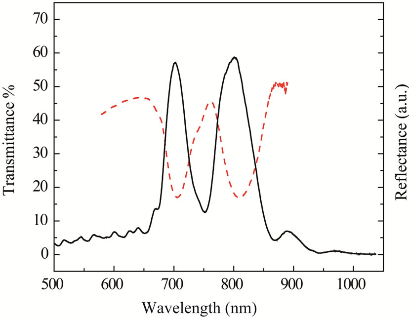
Figure 3. Transmittance (dashed line) and reflectance (solid line) spectra of the heterostructure HT_350-PS/320- SiO2; the peaks centered at about 800 and 700 nm are attributed to the top (PS) and bottom (SiO2) layers, respectively.
measurements performed on HT_350-PS/320-SiO2 system where we can clearly observe the presence of a double peak centered at about 800 and 700 nm, indicating the realization of the heterostructure. Furthermore the position of the stop bands of the double layers HT matches the position of the stop band of each single layer.
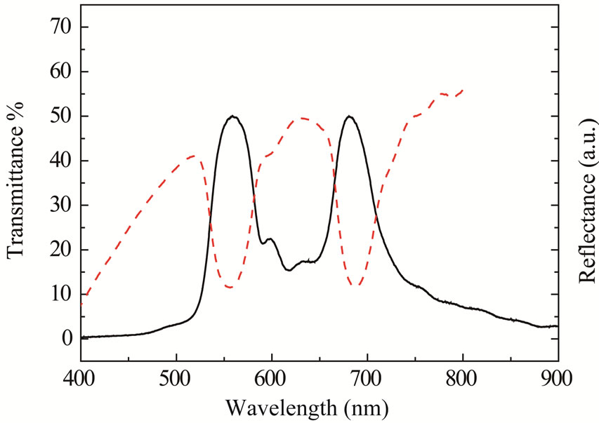
Figure 4. Transmittance (dashed line) and reflectance (solid line) spectra of the heterostructure HT_230-PS/320-SiO2 where the peaks centered at about 550 and 700 nm are attributed to the top (PS) and bottom (SiO2) layers, respectively.
This behaviour can be seen as just a superposition of the properties of each individual layer [19].
Moreover, we have verified that the approach used permits to obtain heterostructure systems based on the deposition of smaller NPs on bigger ones (HT_230-PS/320- SiO2). In fact in Figure 4 we report the transmittance and reflectance spectra obtained on these heterostructure.
Analysing Figure 4 we can notice the presence of a double peak centered at about 550 and 700 nm. These peaks match the position of the stop band of each single layer (Figure 1) that compose the heterostructure; confirming that the method used permits to deposit colloidal crystals constituted by smaller NPs on bigger ones. Moreover we can affirm that the protocol developed permit to obtain an improvement in term of optical properties of the heterostructures realized respect to some of the recent results published by Piret and Khokhar [27,34].
4. Conclusion
We have demonstrated a suitable protocol for the realization of opal photonic crystal heterostructures based on multilayer deposition of silica and polystyrene colloidal films. This method permits to deposit on a silica opal, polymeric colloidal crystals with different lattice constant. In fact SEM images performed on the two HTs realized (HT_350-PS/320-SiO2 and HT_230-PS/320- SiO2) have shown a good ordering of the two-layer colloidal crystals and large domains for the top layer. The double photonic stop bands observed in the reflectance and transmission measurements confirm the formation of the HT system. Moreover the position of the stop bands of heterostructures matches the position of the stop band of single layers; this behaviour can be seen as just a superposition of the properties of each individual layer. Further investigations are in progress in order to minimize the effect of the roughness at interface that is responsible of the reduction of the optical quality of the heterostructures compared with each single opal system.
5. Acknowledgements
This research was performed in the framework of the CARITRO project.
REFERENCES
- E. Yablonovitch and T. J. Gmitter, “Photonic Band Structure: The Face-Centered-Cubic Case,” Physical Review Letters, Vol. 63, No. 18, 1989, pp. 1950-1953. doi:10.1103/PhysRevLett.63.1950
- S. John, “Strong Localization of Photons in Certain Disordered Dielectric Superlattices,” Physical Review Letters, Vol. 58, No. 23, 1987, pp. 2486-2489. doi:10.1103/PhysRevLett.58.2486
- Y. Li, L. M. Fortes, A. Chiappini, M. Ferrari and R. M. Almeida, “High Quality Factor Er-Doped Fabry-Perot Microcavities by Sol-Gel Processing,” Journal of Physics D-Applied Physics, Vol. 42, No. 20, 2009, pp. 205104- 1-205104-7. doi:10.1088/0022-3727/42/20/205104
- T. F. Krauss, R. M. De La Rue and S. Brand “Two-Dimen-Sional Photonic-Bandgap Structures Operating at Near-Infrared Wavelengths,” Nature, Vol. 383, No. 24, 1996, pp. 699-702. doi:10.1038/383699a0
- A. Blanco, E. Chomski, S. Grabtchak, M. Ibisate, S. John, S. W. Leonard, C. Lopez, F. Meseguer, H. Miguez, J. P. Mondla, G. A. Ozin, O. Toader and H. M. Van Driel, “Large-Scale Synthesis of a Silicon Photonic Crystal with a Complete Three-Dimensional Bandgap Near 1.5 Micrometres,” Nature, Vol. 405, No. 25, 2000, pp. 437-440. doi:10.1038/35013024
- V. Morandi, F. Marabelli, V. Amendola, M. Meneghetti and D. Comoretto, “Colloidal Photonic Crystals Doped with Gold Nanoparticles: Spectroscopy and Optical Switching Properties,” Advanced Functional Materials, Vol. 17, No. 17, 2007, pp. 2779-2786. doi:10.1002/adfm.200600764
- H. Fudouzi and T. Sawada, “Photonic Rubber Sheets with Tunable Color by Elastic Deformation,” Langmuir, Vol. 22, No. 3, 2006, pp. 1365-1368. doi:10.1021/la0521037
- D. Zonta, A. Chiappini, A. Chiasera, M. Ferrari, M. Pozzi, L. Battisti and M. Benedetti, “Photonic Crystals for Monitoring Fatigue Phenomena in Steel Structures,” SPIE Proceedings of Sensors and Smart Structures Technologies for Civil, Mechanical, and Aerospace Systems, San Diego, 9-12 March 2009, Article ID: 729215. doi:10.1117/12.814915
- Z. Z. Gu, R. Horie, S. Kubo, Y. Yamada, A. Fujishima and O. Sato, “Fabrication of a Metal-Coated Three-Dimen-Sionally Ordered Macroporous Film and Its Application as a Refractive Index Sensor,” Angewandte Chemie-International Edition, Vol. 41, No. 7, 2002, pp. 1154- 1156. doi:10.1002/1521-3773(20020402)
- L. Lu, I. Randjelovic, R. Capek, N. Gaponik, J. Yang, H. Zhang and A. Eychmüller, “Controlled Fabrication of Gold-Coated 3D Ordered Colloidal Crystal Films and Their Application in Surface-Enhanced Raman Spectroscopy,” Chemistry of Materials, Vol. 17, No. 23, 2005, pp. 5731-5736. doi:10.1021/cm051473d
- A. Chiappini, S. Guddala, C. Armellini, S. Berneschi, I. Cacciari, C. Duverger-Arfuso, M. Ferrari and G. C. Righini, “Fabrication and Characterization of Colloidal Crystals Infiltrated with Metallic Nanoparticles,” SPIE Proceedings of the International Society for Optical Engineering, San Diego, 1-5 August 2010, Article ID: 77250W.
- M. Scharrer, A. Yamilov, X. Wu, H. Cao and R. P. H. Chang, “Ultraviolet Lasing in High-Order Bands of ThreeDimensional ZnO Photonic Crystals,” Applied Physics Letters, Vol. 88, No. 20, 2006, pp. 201103-1-201103-3. doi:10.1063/1.2203939
- A. Chiappini, C. Armellini, A. Chiasera, M. Ferrari, Y. Jestin, M. Mattarelli, M. Montagna, E. Moser, G. Nunzi Conti, S. Pelli, G. C. Righini, C. M. Gonçalves and R. M. Almeida, “Design of Photonic Structures by Sol-Gel Derived Silica Nanospheres,” Journal of Non-Crystalline Solids, Vol. 353, No. 5-7, 2007, pp. 674-678. doi:10.1016/j.jnoncrysol.2006.10.034
- A. C. Arsenault, D. P. Puzzo, I. Manners and G. A. Ozin, “Photonic-Crystal Full-Colour Displays,” Nature Photonics, Vol. 1, No. 8, 2007, pp. 468-472.
- F. Li, D. P. Josephson and A. Stein, “Colloidal Assembly: The Road from Particles to Colloidal Molecules and Crystals,” Angewandte Chemie-International Edition, Vol. 50, No. 2, 2011, pp. 360-388. doi:10.1002/anie.201001451
- H. Fudouzi, “Novel Coating Method for Artificial Opal Films and Its Process Analysis,” Colloids and Surfaces A: Physicochemical and Engineering Aspects, Vol. 311, No. 1, 2007, pp. 11-15. doi:10.1016/j.colsurfa.2007.08.034
- L. V. Woodcock, “Entropy Difference between the FaceCentred Cubic and Hexagonal Close-Packed Crystal Structures,” Nature, Vol. 385, 1997, pp. 141-143. doi:10.1038/385141a0
- H. Míguez, C. López, F. Meseguer, A. Blanco, L. Vázquez, R. Mayoral, M. Ocaña, V. Fornés and A. Mifsud, “Photonic Crystal Properties of Packed Submicrometric SiO2 Spheres,” Applied Physics Letters, Vol. 71, No. 9, 1997, pp. 1148-1150. doi:10.1063/1.119849
- P. Jiang, G. N. Ostojic, R. Narat, D. M. Mittleman and V. L. Colvin, “The Fabrication and Bandgap Engineering of Photonic Multilayers,” Advanced Materials, Vol. 13, No. 6, 2001, pp. 389-393. doi:10.1002/1521-4095(200103)
- W. Khunsin, S. G. Romanov, C. M. Sotomayor Torres, J. Ye and R. Zentel, “Optical Transmission in Triple-Film Hetero-Opals,” Journal of Applied Physics, Vol. 104, No. 1, 2008, Article ID: 013527. doi:10.1063/1.2951958
- B. Ding, M. Bardosova, I. Povey, M. E. Pemble and S. G. Romanov, “Engineered Light Scattering in Colloidal Photonic Heterocrystals,” Advanced Functional Materials, Vol. 20, No. 5, 2010, pp. 853-860. doi:10.1002/adfm.200901319
- N. Stefanou, V. Yannopapas and A. Modinos, “MULTEM 2: A New Version of the Program for Transmission and BandStructure Calculations of Photonic Crystals,” Computer Physics Communications, Vol. 132, No. 1-2, 2000, pp. 189- 196. doi:10.1016/S0010-4655(00)00131-4
- Q. Yan, L. K. Teh, Q. Shao, C. C. Wong and Y.-M. Chiang, “Layer Transfer Approach to Opaline Hetero Photonic Crystals,” Langmuir, Vol. 24, No. 5, 2008, pp. 1796-1800. doi:10.1021/la702668p
- D. K. Hwang, H. Noh, H. Cao and R. P. H. Chang, “Photonic Bandgap Engineering with Inverse Opal Multi-Stacks of Different Refractive Index Contrasts,” Applied Physics Letters, Vol. 95, No. 9, 2009, pp. 091101-1-091101-3.
- M. Eegn, R. Voss, B. Griesebock and R. Zentel, “Heterostructures of Polymer Photonic Crystal Films,” Chemistry of Materials, Vol. 15, No. 20, 2003, pp. 3786-3792. doi:10.1021/cm030087y
- R. V. Nair and R. Vijayaa, “Three-Dimensionally Ordered Photonic Crystal Heterostructures with a Double Photonic Stop Band,” Journal of Applied Physics, Vol. 102, No. 5, 2007, pp. 056102-1-056102-3. doi:10.1063/1.2777120
- F. Piret, Y.-U. Kwon and B.-L. Su, “Silica Colloidal Crystals with Uniand Multi-Photonic Bandgaps and Controlled Reflective Properties,” Chemical Physics Letters, Vol. 472, No. 4-6, 2009, pp. 207-211. doi:10.1016/j.cplett.2009.03.014
- A.-J. Wang, S. L. Chen, P. Dong, X. G. Cai, Q. Zhou, G. M. Yuan, C. T. Hu and D. Z. Zhng, “Fabrication of Colloidal Photonic Crystals with Heterostructure by SpinCoating Method,” Chinese Physics Letters, Vol. 26, No. 2, 2009, pp. 024210-1-024210-4. doi:10.1088/0256-307X/26/2/024210
- W. Stober, A. Fink and E. Bohn, “Controlled Growth of Monodisperse Silica Spheres in the Micron Size Range,” Journal of Colloid and Interface Science, Vol. 26, No. 1, 1968, pp. 62-69. doi:10.1016/0021-9797(68)90272-5
- B. T. Holland, C. F. Blanford, T. Do and A. Stein, “Synthesis of Highly Ordered, Three-Dimensional, Macroporous Structures of Amorphous or Crystalline Inorganic Oxides, Phosphates, and Hybrid Composites,” Chemistry of Materials, Vol. 11, No. 3, 1999, pp. 795-805. doi:10.1021/cm980666g
- A. Chiappini, C. Armellini, A. Chiasera, M. Ferrari, L. Fortes, M. Clara Gonçalves, R. Guider, Y. Jestin, R. Retoux, G. Nunzi Conti, S. Pelli, R. M. Almeida and G. C. Righini, “An Alternative Method to Obtain Direct Opal Photonic Crystal Structures,” Journal of Non-Crystalline Solids, Vol. 355, No. 18, 2009, pp. 1167-1170. doi:10.1016/j.jnoncrysol.2009.01.054
- P. Jiang, J. F. Bertone, K. S. Hwang and V. L. Colvin, “Single-Crystal Colloidal Multilayers of Controlled Thickness,” Chemistry of Materials, Vol. 11, No. 8, 1999, pp. 2132-2140. doi:10.1021/cm990080+
- G. Johnson and J. Joannopoulos, “Block-Iterative Frequency-Domain Methods for Maxwell’s Equations in a Planewave Basis,” Optics Express, Vol. 8, No. 3, 2001, pp. 173-190. doi:10.1364/OE.8.000173
- A. Z. Khokhar, F. Rahman and N. P. Johnson, “Photonic Crystal Heterostructures from Self-Assembled Opals,” Applied Physics A: Materials Science and Processing, Vol. 102, No. 2, 2011, pp. 281-287. doi:10.1007/s00339-010-6145-7
NOTES
*Corresponding author.