Open Journal of Applied Sciences
Vol.3 No.1(2013), Article ID:29560,9 pages DOI:10.4236/ojapps.2013.31019
Fabrication Parameter Optimization for a Multilayer Photovoltaic Cell Based on the Heterojunction: Zinc(II)-Meso-Tetrakis(4-Bromophenyl) Porphyrins/Fullerenes
1Laboratorio de Polímeros Conductores, Departamento de Química y Biología, Universidad de Santiago de Chile, Santiago, Chile
2Laboratorio de Electroquímica de Polímeros, Departamento de Química Inorgánica, Facultad de Química, Pontificia Universidad Católica de Chile, Santiago, Chile
3Institut des Matériaux Jean Rouxel (IMN), Université de Nantes, Nantes, France
4MOLTECH-Anjou, Université d’Angers, Angers, France
5Faculté des Sciences, Unité de Recherche Associé, Laboratoire Optoélectronique et Physico-Chimie des Matériaux, Kenitra, Morocco
Email: *jorge.velez@usach.cl
Received August 31, 2012; revised November 2, 2012; accepted November 12, 2012
Keywords: Conducting Polymers; Phorphyrin Reactivity; Photovoltaic Yield; Anode Buffer Layer; CuI; MoO3
ABSTRACT
The photoelectric properties of multilayer organic photovoltaic cells (OPV cells) were studied. The active organic layers consisted of a planar heterojunction between a layer of Meso-Tetrakis(4-BromoPhenyl) Zinc(II) Porphyrin (BrPhPZn) as electron donor (ED) and a layer fullerene molecules. The devices were fabricated in a high vacuum by thermal sublimation, a technique that allows multilayer devices realization easily by successive depositions, and it does not require solvents, achieving purer films with reproducible characteristics. Taking into account that the anodic contact, a key factor for cell efficiency, is favored by the inclusion of a thin anodic buffer layer (ABL), the effect on the yield after including one or two (ABL): MoO3 or MoO3-CuI layers was studied. The cell which has the best photovoltaic characteristics has a BrPhPZn (ED) thickness of only 12.5 nm. This small thickness is related with the low conductivity of this organic molecule. On the other hand, including a thin MoO3-CuI bilayer increased, such device’s efficiency in a 200%, with regard to a cell without ABL, getting for one cell ITO/MoO3-CuI/BrPhPZn/C60/Alq3/Al, with a 1.03% yield.
1. Introduction
Organic photovoltaic cells (OPV cells) [1-3] mainly consist of conjugated polymers, conjugated polymers mixes, and conjugated molecules. These materials offer a great compatibility with the environment due to their degradeability. The first molecular semiconductor which was known is the lutetium phthalocyanine, (Ft2Lu) [4]. Most of organic molecular semiconductors that are known today consist of highly ordered alignments of donor and acceptor species, where one or both of them are thermodynamically stable ionic radicals. Amongst those, there are the partially oxidized by iodine phthalocyanines and porphyrins [4]. In most of the complexes which are constituted by these ligands (phthalocyanines and porphyrins) and different transition metals, semi conductive properties can be observed except for the nickel(I) phthalocyanines. According to these antecedents, a Zn, Zinc(II)- Meso-Tetrakis (4_bromoPhenyl), porphyrin was prepared, and it turned out to be a good semiconductor and it was tested as electron donor (ED) layer to obtain a high efficiency solar cell. On the other hand, porphyrin-fullerene heterojunction was studied because previous research [5], has demonstrated that, when a little amount of C60 is introduced in a polymeric system, many of the characteristics of the related polymers are enhanced, such as photoconductivity [5], mechanical properties [6], optical properties [7], etc. In the previous research conducted by our group, it was possible to determine that a 40 nm fullerene layer increases the efficiency of this kind of devices [8]. The combination of these materials has drawn special interest after the discovery of the fast photoinduced electrons transference from organic polymers to fullerenes, which are excellent electron acceptors (EA).
Therefore, in this research, photoelectric properties of photovoltaic devices based on the organic heterojunction porphyrin—C60 organic and the effect on such devices of the insertion of an anode buffer layer (ABL) have been studied.
The devices were fabricated in a sandwich-like structure. The thickness of the active layers influences optically and electrically the efficiency response. For this reason, the relations of the photocurrent and the current density-tension characteristics versus the active layer thickness were studied. The thickness of the active layers influences optically and electrically the efficiency response.
The optic properties were obtained by measuring the adsorption spectra and the photovoltaic properties were obtained by measuring the current density-tension characteristic curves in the dark and under cell illumination The devices were fabricated by in a high vacuum by thermal sublimation, a technique that allows multilayer formation by successive depositions, in a sandwich-like structure. This technique does not require solvents, achieving purer films with reproducible characteristics.
On the other hand, for the OPVs Cells to function it is needed that the material absorbs photons which energy equal or surpasses that of the gap of the absorbent organic layer, so the electrons are promoted from the highest occupied molecular orbital (HOMO) to the lowest unoccupied molecular orbital (LUMO). Then, the induced hole in the HOMO and the electron in the LUMO form a couple of charge carriers bound by Coulumbic attraction, named “exciton”. In the formation of electric current, these excitons must be dissociated as free charges. This charge separation is effective at the interface between the ED, here the porphyrin, and the EA, here the C60. Then these free charges must be collected by the electrodes. The anode used is the transparent ITO and the cathode is an aluminium film. With the idea of improving the efficiency and taking into account that the anodic contact plays an important role in such aspect, it has been found that the introduction of a thing layer between the ITO and the electron donor layer, called anodic buffer layer (ABL), will increase the yield of OPVs. In the present work, the inclusion of a thin monolayer of MoO3 or of a bilayer MoO3-CuI was studied, in which the inclusion of a MoO3-CuI bilayer showed the best results.
2. Experimental Details
2.1. Chemical Reactives
All the reactives and solvents used where pro analysis quality or better: pyrrole and 4-Bromobenzaldehyde for synthesis were obtained from Sigma-Aldrich; propionic acid, hexane, chloroform, ethanol, methanol, sodium hydroxide, acetone, acetic acid 100%, boric acid, orthophosphoric acid 85%, silica gel 60 230 - 400 mesh ASTM, 0.04 - 0.063 mm porosity, cobalt acetate (II), deuterated chloroform and sodium sulfite were from Merck; potassium chloride was obtained from Riedelde-Haen; tetrabutylammonium perchlorate 99% from Across-Organics; silicone oil from Vetec; dichloromethane from J.T Baker; and ultra pure nitrogen 99.995 from AGA.
2.2. Instruments
Microanalysis was performed on a Fison, Model EA- 1108, elemental analyzer. Proton nuclear magnetic resonance spectra (1H-NMR) were registered in a Brucker Advance 400 MHz spectrometer and processed by Mestrec software. UV-visible electronic spectra were registered in a Scinco S-3100 spectrophotometer, which has a diode bridge detector on 1 cm optical pass quartz cell. The equipment is controlled by the LabPro software through an interface. The spectrum window was 350 to 750 mm. All the measurements were taken in dichloromethane at room temperature.
The monomer films were prepared by thermal sublimation in high vacuum at 1 × 10⁻⁴ Pa of pressure at the same time as the photovoltaic devices. The deposit rate of each monomer was 0.5 Å·s–1. In order to investigate the optical behavior at the same conditions than the solar cell, the optical properties were determined in thin film solid state (optical density O.D).
The photovoltaic devices were assembled in a multi heterojunction structure as follows: indium tin oxide (ITO)/anode buffer layer MoO3 and/or CuI/BrPhPZn/ fullerene (C60)//Alq3/Al. The devices were prepared by sublimation at 1 × 10⁻⁴ Pa. The thin film deposition rates and thickness were estimated in situ through a quartz monitor. Electrical characterizations were performed with an automated I-V tester, in the dark and under sun global AM 1.5 simulated solar illuminations. Performances of photovoltaic cells were measured using a calibrated solar simulator (Oriel 300 W) at 100 mW/cm2 light intensity.
The characteristics of the photovoltaic cells were measured using a calibrated solar simulator (Oriel 300 W) at 100 mW/cm2 light intensity adjusted with a reference cell (0.5 cm2 CIGS solar cell, calibrated at NREL, USA).
The thin film structures are analyzed by X ray diffraction (XRD) by a Siemens D5000 diffractometer using Kα radiation from Cu (λKα = 0.15406 nm).
2.3. Synthesis of Meso-Tetrakis (4-Bromophenyl) Porphiryn (H2BrPhP)
The complex was synthesized according to Adler Method described in literature [9]. 4-Bromobenzaldehyde (3.9 g, 21 mmol) and pyrrole (1.5 mL, 21 mmol) in 150 mL of propionic acid were heated by reflux. After 30 minutes, the formation of a black precipitate was observed. It was cooled at room temperature, and methanol was added, cooling it by an ice bath at 0˚C during 15 min. Subsequently, it was filtered and the filtrand was washed with distillated water and methanol, dried and later purified by column chromatography (silica/CH2Cl2), obtaining a solid and crystalline purple precipitate (34% yield): Elemental analysis: C44H26N4Br4 (H2BrPhP); calculated: C: 56.97, H: 2.83, N: 6.04; found: C: 57.01, H: 2.80, N: 6.02. 1HNMR (400 MHz, CDCl3) H2BrPhP: d 8.80 (s, 8H), 8.02 (d, 8H), 7.96 (d, 8H), –2.98 (2H).
2.4. Metalation of of Meso-Tetrakis (4-Bromophenyl) Porphiryn (H2BrPhP)
H2BrPhP (2.33 g, 2.5 mmol) and copper acetate monohydrate (1.99 g, 10 mmol) in dichloromethane and ethanol (1:1) were placed in a Schlenk reactor to be purged with argon for 5 minutes and later heated by reflux for 6 hours. The obtained violet solution was cooled at room temperature and its organic phase was extracted by dichloromethane and water. The organic phase was dried with sodium sulfate anhydride which was filtered afterwards. The product that contains the metallated porphyrin was dried before being purified by silica gel column chromatography, and the significant compound was eluted with a mixture of dichloromethane:hexane (3:1). The product obtained is violet colored and has a 65% yield: C44H24N4Br4Zn (BrPhPZn).
2.5. Thin Films Characterization
In order to understand the effect of the different ABL on the OPV cells performances, different characterization techniques have been used for studying the structures ITO/ABL and ITO/ABL/BrPhPZn.
Thin films structures were analyzed by X ray diffracttion (XRD) by a Siemens D5000 diffractometer using Kα radiation from Cu (λKα = 0.15406 nm).
Optical measurements were carried out at room temperature using a Carry spectrometer. The film transmittance was measured at wavelengths of 1.2 to 0.30 μm.
Morphology of the different structures used as anode was observed through scanning electron microscopy (SEM) with a JEOL 7600 F at the “Centre de microcaractérisation de l’IMN, Université de Nantes”. Images in secondary (SEM) and backscattering (BEI) mode have been done. Composition of the films were studied by electron probe micro analysis (EPMA), where the scanning electron microscope was equipped with a BRUKER Quantax X-ray microanalysis system; X-rays were detected by a silicone drift detector.
AFM images on different sites of the film were taken ex-situ at atmospheric pressure and room temperature. All measurements have been performed in tapping mode (Nanowizard III, (JPK Instruments). Classical SiN4 cantilevers were used (Ultrasharp, AXESSTECH, France).
The average force constant and resonance were approximately 14 N/m and 320 kHz, respectively. The cantilever was excited at its resonance frequency.
2.6. The Organic Solar Cell
An OPV cell needs a transparent conductive electrode which allows the photons to reach the photoactive layer. Here, the glass substrate is coated with 100 nm of a conductive oxide, the indium and tin oxide. The photoactive components are displayed as nm-thin layers. Between the transparent anode and the ED a mono or bi ABL (MoO3 or MoO3-CuI) is placed, which increases the photovoltaic device efficiency through an improvement of the band matching at the interface anode/electron donor. The next layer is constituted by the photoactive material or electron donor compound (ED), meso-tetrakis (4-Bromophenyl)zinc porphiryn (BrPhPZn) [10-12]. On this layer a layer of the electron acceptor material, which are generated by the fullerene photoactive material C60, is deposited. Actually, C60 has a high electroafinity value, which makes it a good electron acceptor and also exhibits satisfying conductivity (10–4·Scm–1) [13-15]. Afterwards, a tris-8-hydroxyquinoline aluminum, Alq3, layer is placed, which is a very efficient organometallic complex with great stability and it is used as exciton blocking layer. Finally, the cathode, often is a thin aluminium layer (100 nm), is deposited by thermal evaporation through a mask with 1 mm × 10 mm active areas (Diagram 1).
According to this diagram, sun photons would go through the transparent electrode and would be absorbed into the device by the active organic layer, BrPhPZn, which leads to the generation of the exiton (for the electron hole) [15,16].
3. Solar Cells Characterization
3.1. Curves I-V
The characterization of the cells was carried out by a common method for fotovoltaic cells [17,18], which is based on the determination of a series of parameters such as open circuit voltages (Voc), current density intensity in short-circuit (Isc), the fill factor FF), and the efficiency of the luminous energy conversion. The intersecttion of the I-V curves and the abscissa axis gives the open-circuit voltage value (Voc) and the intersection with the coordinates axis gives the value of the current density in short-circuit (Isc). The maximum power will
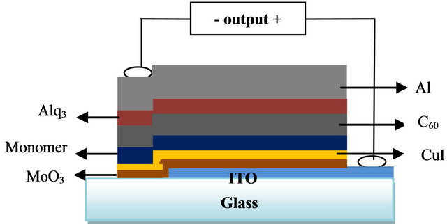
Diagram 1. Typical structure of an organic solar cell (ITO/ MoO3-CuI/BrTPP(Zn) (4-Bromophenyl zinc porphiryn)/ C60/Al.
be the maximum product of the product IxV.
A typical result is shown in Figure 1.
3.2. Characterization of a Photovoltaic Cell, ABLs
The insertion of a thin anodic buffer layer, ABL, favors the anodic contact between ITO and the ED, which plays an important role in the photovoltaic cells efficiency. One of the most commonly used ABL corresponds to transition metal oxides: MoO3, V2O5, WO3, that are highly transparent and which have been successfully used to modify the anodic surface. The thickness of such metal oxide is important. A too thin ABL leads to inhomogeneous properties at the interface anode/ED by incomplete surface coating [19], while a too thick layer increases the serial resistance (Rs) and therefore reduces Jsc and FF. We have already shown that, in the experimental conditions used in this work, the optimum thickness of the MoO3 ABL is 3 nm [20].
It is known that such MoO3 ABL allows achieving good band matching at the interface anode/ED. Actually, much research has been dedicated to the adjusting of the band matching to reduce the barrier at the interface anode/electron donor through the introduction of an ABL
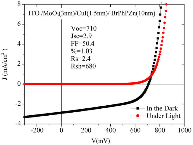
Figure 1. Photovoltaic characterization of the structure of an organic solar cell (ITO: indium and tin oxide, MoO3 (3 nm)/CuI (1.5 nm)/BrTPhP(Zn) (10 nm)/C60 (70 nm)/Al (100 nm)).
[20-24].
No much research has been devoted to the effect of the surface energy of the anode on the structure and morphology of the organic films [25,26]. However, the carrier transport properties of the organic semiconductor comprising π-conjugated molecules strongly depend on the molecular order in the films. So it could be of interest to use an ABL which not only improves the band matching at the interface, but also allows some improvement of the order in the absorbing organic layer. Recently, it has been shown that CuI can be used to control the molecular orientation of metal phthalocyanine (MPc) in organic cells based on MPc/C60 [27-29] Therefore, in the present research we extend the study to the effect of CuI on the performances of organic cells based on multi-heterojunction using porphyrin as electron donor through double ABL: MoO3-CuI.
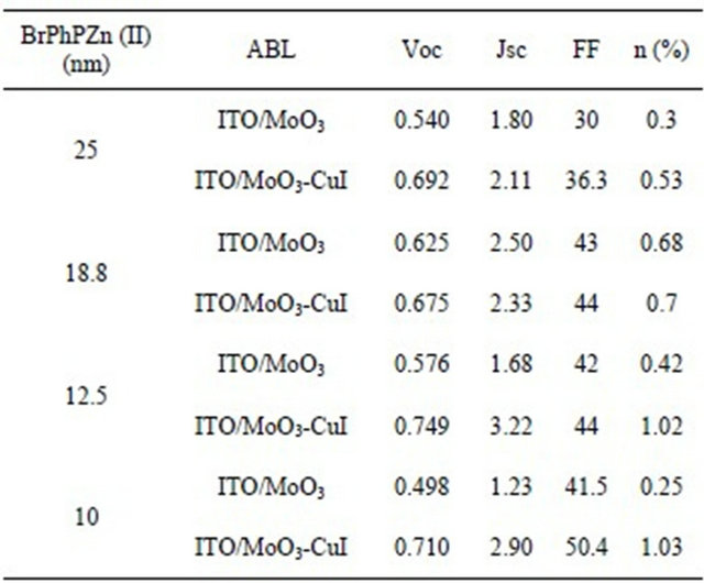
As it can be seen in the results showed in Table 1, the insertion of the double MoO3-CuI ABL increases the yield of organic photovoltaic cells (OPV) close to the double of magnitude if compared to the device prepared with a mono layer of MoO3.
It is important to point out that the improvement by the insertion of a thin CuI layer is strongly related with the improvement of Voc and Jsc while there is no significant evolution of FF.
We show in the Table 1 that, whatever the thickness of the BrPhPZn, the MoO3-CuI ABL allows improving the solar cells performances. We will discuss more precisely the influence of the BrPhPZn below.
3.3. Thickness of the BrPhPZn Film
The study of the effect of the thickness of the porphyrin film, BrPhPZn, on the efficiency of the organic photo-
Table 1. Characterization of a photovoltaic cell, ABLs.
voltaic cells (OPV cells) is summed up in Table 2. The device which showed the highest efficiency was the one with a BrPhPZn film thickness of 12.5 nm. For thinner films (10 nm), there is no more improvement of the cells performances. For BrPhPZn layers thick of 50 nm it is observed that the Jsc and Voc values are low, and they increase gradually as the film thickness diminishes. This response could be related to the low conductivity and hole mobility of the compound [19].
3.4. Characterization of a Photovoltaic Cell, Thickness of the CuI Film
The thickness value of CuI, directly influences the efficiency of the prepared devices, as the results in Table 3 show. It tells that the best performances are obtained with a CuI thickness of 1.5 nm. This thickness allows achieving the best compromise between a small series resistance Rs and an acceptable shunt resistance Rsh. This compromise allows to increase significantly Jsc without much affect the value of Voc.
In order to try to understand the influence of CuI and MoO3 on the performances of the OPV cells, we have submitted the structures: ITO/CuI/BrPhZn, ITO/MoO3/ BrPhZn and ITO/MoO3-CuI/BrPhZn to some specific characterization techniques.
First of all, the BrPhZn layers obtained are amorphous, whatever the anode configurations, with or without ABL.
The absorption of the BrPhZn films (20 nm) deposited onto ITO and the different ABL is reported in Figure 2. Figure 2 shows the expected Soret and Q bands for the metaled complex. The Soret intense absorption band (β) in the 400 nm to 430 nm region, these bands are characteristic for porphyrins and are due to π – π* ligand transitions [30]. Over the 500 nm, 2 bands (Q) can be observed due to zinc insertion in the porphyrin ring, which generates an increase of the symmetry (from D2h to D4h).
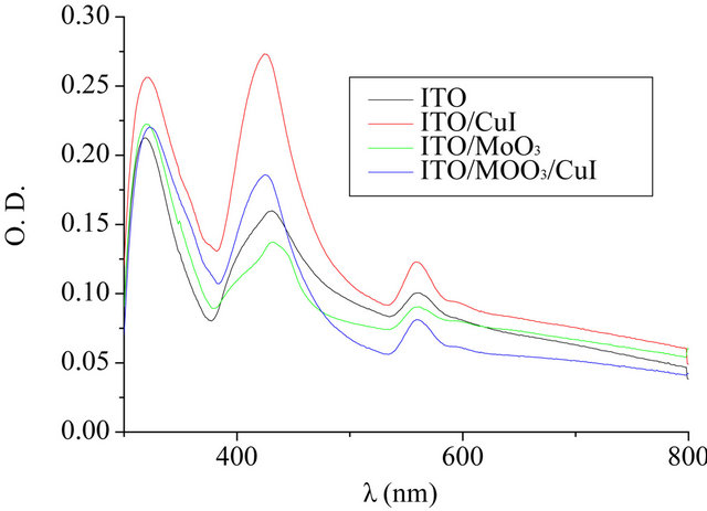
Figure 2. Optical density spectrum of BrPhZn thin films (20 nm) deposited onto different anodes.
We can see that the optical density of films deposited onto CuI is significantly higher than that of films deposited onto ITO. Moreover, the absorption of the film deposited on MoO3 is less than when it is deposited on ITO, but the introduction of a CuI layer onto MoO3 increases this absorption.
These results could justify, at least partly, the improvement of the OPV cells performances induced by the double MoO3/CuI ABL.
In order to determine the effect of the different ABLs on the BrPhZn film conductivity, we have investigated the J-V characteristics of hole-only devices with MoO3, CuI and MoO3/CuI ABL. These devices were grown using high work-function electrode buffer layers. The hole only devices were fabricated by replacing the C60 and the BCP EBL with high work function MoO3, which is well known to be a hole injector (collector) and a blocking electron layer. Hole only devices have been made using the same ITO covered glass substrate than those used to grow OPV cells. After deposition of the ABL, a BrPhZn film thick of 30 nm has been deposited. Then the organic film has been covered with a MoO3 film thick of 7 nm. Finally aluminium has been used as top electrode. The J-V characteristics of the hole only devices are shown in Figure 3. Charge transport in these devices is limited to holes. Electron injection from the aluminum electrode can be neglected, due to the large electron bar rier due to the MoO3 interlayer.
The devices using CuI ABL show largest current density at the same driving voltages as compared to the devices using MoO3 ABL. Clearly the conductivity is enhanced by an order of magnitude when a CuI/MoO3 ABL is used on the place of the MoO3 ABL. All the devices display near ohmic transport at low voltage. Actually, in the low voltage range, ohmic contacts can be seen by the linear relation between the current density J and the voltage V at higher current density the slope increases
Tabla 2. Characterization of a photovoltaic cell, thickness of the BrPhPZn film.
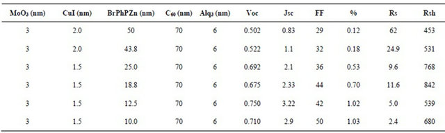
Table 3. Characterization of a photovoltaic cell, thickness of the CuI film.
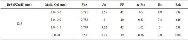
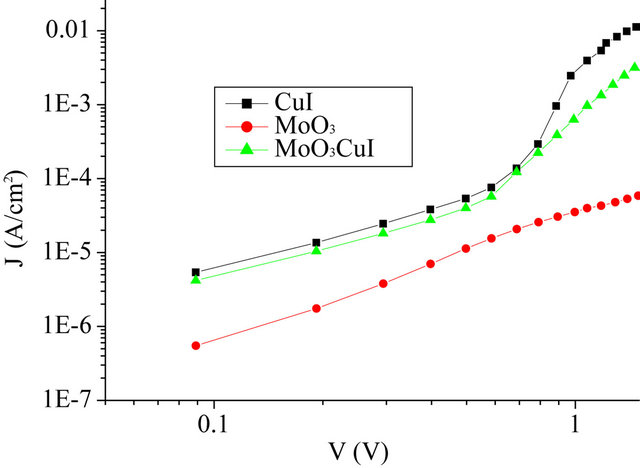
Figure 3. Log-log plot of the current density-voltage curves of the whole only devices.
which corresponds to a transition towards Space Charge Limited Current (SCLC) which is often obtained in such devices [30].
The studies of the layer morphology by scanning electron microscopy (SEM) and atomic force microscopy (AFM) allow to determine the rugosity and superficial characteristics of the donor organic layer, BrPhPZn, which will depend on the ABL layer in contact with the latter.
The visualization of the layers under the scanning microscope allows to see butterfly-shaped “features”, which are scattered over the surface See Figure 4.
In Figure 5, on the other hand, we can see that the
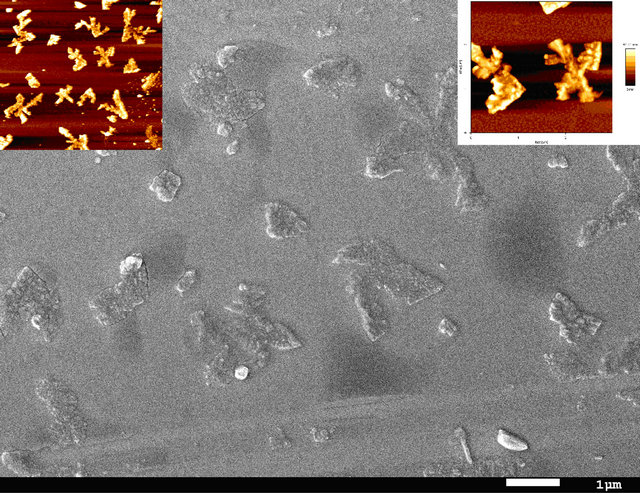
Figure 4. SEM and AFM for film of MoO3/BrPhZn.
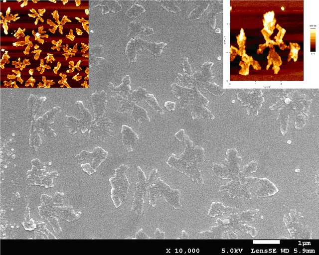
Figure 5. SEM and AFM for film of MoO3/CuI/BrPhZn.
concentration or population density of these “butterfly-like” morphologies is higher with CuI, which can be proved with the AFM. In Figures 6 and 7 we have measured the rugosity, which can be clearly seen in tridimensional images with the AFM, the Rms over MoO3/CuI = 15 nm, and over MoO3 el Rms = 16 nm, that is to say that is more or less the same rugosity, what changes is the density of these “butterfly” kind of formations. The cross sections make it possible to see the different densities of rugosity.
According to these results, it can be seen that the morphological determination by SEM and AFM allows for a clear sight of the influence of the blocking layer (MoO3 or CuI) over the growth of the organic layer. This differ-
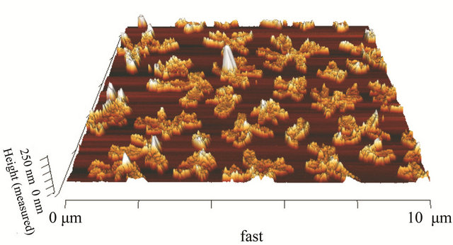

Figure 6. SEM and AFM for film of CuI/BrPhZn.

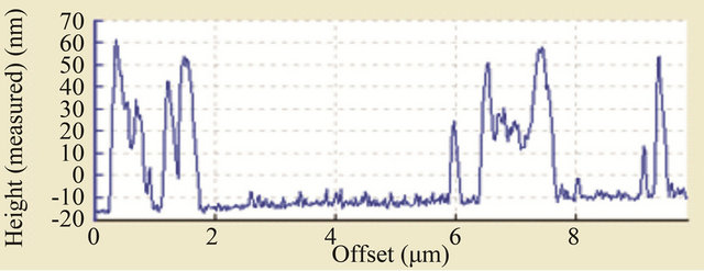
Figure 7. SEM and AFM for film of MoO3/BrPhZn.
ent growth allows the understanding of the differences in the conductivities of the layers deposited over CuI. The increase in the yield of the cells that used CuIO as ABL would be because of the increase in the conductivity of the donor layer for the introduction of CuI.
According to these results, it can be seen that the morphological determination by SEM and AFM allows for a clear sight of the influence of the blocking layer (MoO3 or CuI) over the growth of the organic layer. This different growth allows the understanding of the differences in the conductivities of the layers deposited over CuI. The increase in the yield of the cells that used CuIO as ABL would be because of the increase in the conductivity of the donor layer for the introduction of CuI.
Another limiting factor affecting power conversion efficiency is the small diffusion length of the exciton before recombination. Typical diffusion lengths of exciton are in the range of 10 nm. So, it is necessary to improve the interface area between the electron donor and the electron acceptor in order to improve the probability of charge separation. A possible approach to achieve a large interface area is the use of a quite rough active organic layer. In the present case, the higher density of rough feature in the case of CuI ABL can participate to the improvement of the photocurrent.
Ÿ 4. Conclusions
Ÿ The device that showed the highest quantum efficiency (IPCE) was the one with the thinnest thickness where the system still describes electric behavior (12.5 nm and 10 nm). For thick layers of the 50 nm compound it was observed that the Jsc and Voc values are low, and they gradually increase as the film gets thinner.
Ÿ The anodic contact, ITO, plays a key role in the OPV cells yield, therefore the introduction of an anodic buffer layer (ABL), MoO3-CuI, improves the efficiency of the latter, getting a yield that is close to duplicate the yield that is obtained when they are prepared with a MoO3 monolayer, showing an increase on the open-circuit voltage (Voc) and the short-circuit current (Jsc).
The thickness of the ABL layer, CuI plays an important role in photovoltaic devices yield, a layer that is too thin leads to less open-circuit power (Voc) and to an increase in the leakage current by incomplete surface coating, while a layer that is too thick increases the serial resistance (Rs) and reduces the short-circuit power (Jsc).
5. Acknowledgements
The authors thank proyect Fondecyt 3100066. Fondecyt 1120071, Dicyt-Usach and proyect ECOS-CONICYT. N˚C09E02.
REFERENCES
- J. H. Schoen, C. Kloc, E. Bucher and B. Batlogg, “Efficient Organic Photovoltaic Diodes Based on Doped Pentacene,” Nature (London, United Kingdom), Vol. 422, 2003, p. 93. doi:10.1038/nature01468
- C. M. Atienza, G. Fernandez, L. Sanchez, N. Martin, I. S. Dantas, M. M. Wienk, R. A. J. Janssen, G. M. A. Rahman and D. M. Guldi, “Light Harvesting Tetrafullerene Nanoarray For Organic Solar Cells,” Chemical Communications, Vol. 5, 2006, pp. 514-516. doi:10.1039/b510234k
- V. Lemaur, M. Steel, D. Beljonne, J.-L. Bredas and J. Cornil, “Photoinduced Charge Generation and Recombination Dynamics in Model Donor/Acceptor Pairs for Organic Solar Cell Applications: A Full Quantum-Chemical Treatment,” Journal of the American Chemical Society, Vol. 127, No. 16, 2005, pp. 6077-6086. doi:10.1021/ja042390l
- K. M. Kadish, K. M. Smith and R. Guilard, “Radical Pthalocyanines and Intrinsic Semiconduction,” In: K. M. Kadish, K. M. Smith and R. Guilard, Ed., The Porphyrin Handbook, Volumes 19: Applications of Phthalocyanines, Elsevier, San Diego, 2003, p. 39.
- K. Yoshino, X. H. Yin, K. Muro, S. Kiyomatsu, S. Morita, A. A. Zakhidov, et al., “Marked Enhancement of Photoconductivity and Quenching of Luminescence in Poly(2,5- dialkoxy-p-phenylene vinylene) upon C60 Doping,” Japanese Journal of Applied Physics, Vol. 32, No. 3A, 1993, pp. L357-L360. doi:10.1143/JJAP.32.L357
- A. B. Dalton, S. Collins, E. Munoz, J. M. Razal, V. H. Ebron, J. P. Ferraris, et al., “Super-Tough Carbon-Nanotube Fibres,” Nature, Vol. 423, No. 6941, 2003, p. 703 doi:10.1038/423703a
- Z. V. Vardeny, Z. H. Kafafi and J. Shinar, “Electronic Properties of Fullerene/p-Conjugated Polymer Composites,” In: Z. V. Vardeny, Z. H. Kafafi and J. Shinar, Eds., Optical & Electronic Properties of Fullerenes and Fullerene-based Materials, Marcel Dekker Inc., New York, 2000, pp. 333-365.
- J. C. Bernède, L. Cattin, S. Ouro Djobo, M. Morsli, S. R. B. Kanth, S. Patil, P. Leriche, J. Roncali, A. Godoy, F. R. Diaz and M. A. Del Valle, “Influence of the Highest Occupied Molecular Orbital Energy Level of the Donor Material on the Effectiveness of the Anode Buffer Layer in Organic Solar Cells,” Physica Status Solidi (a), Vol. 208, No. 8, 2011, pp. 1989-1994. doi:10.1002/pssa.201127047
- A. D. Adler, F. R. Longo, J. D. Finarelli, J. Goldmacher, J. Assour and L. Korsakoff, “A Simplified Synthesis for Meso-Tetraphenylporphine,” The Journal of Organic Chemistry, Vol. 32, No. 15, 1967, p. 476. doi:10.1021/jo01288a053
- K. Feldrapp, W. Brutting, M. Schwoerer, M. Brettreich and A. Hirsch, “Photovoltaic Effect in Blend Systems and Heterostructures of Poly(p-phenylenevinylene) and c60,” Synthetic Metals, Vol. 101, No. 1, 1999, pp. 156-157. doi:10.1016/S0379-6779(98)00696-1
- C. J. Brabec, A. Cravino, G. Zerza, N. S. Sariciftci, R. Kiebooms, D. Vanderzande and J. C. Hummelen, “Photoactive Blends of Poly(para-phenylenevinylene) (PPV) with Methanofullerenes from a Novel Precursor: Photophysics and Device Performance,” Journal of Physical Chemistry B, Vol. 105, No. 8, 2001, pp. 1528-1536 doi:10.1021/jp003407z
- M. M. Wienk, J. M. Kroon, W. J. H. Verhees, J. Knol, J. C. Hummelen, P. A. van Hal and R. A. J. Janssen, “Efficient Methano[70]fullerene/MDMO-PPV Bulk Heterojunction Photovoltaic Cells,” Angewandte Chemie, International Edition, Vol. 42, No. 29, 2003, pp. 3371-3375. doi:10.1002/anie.200351647
- C. Melzer, V. V. Krasnikov and G. Hadziioannou, “Organic Donor/Acceptor Photovoltaics: The Role of C 60/Metal Interfaces,” Applied Physics Letters, Vol. 82, No. 18, 2003, pp. 3101-3103. doi:10.1063/1.1570936
- C.-W. Chu, Y. Shao, V. Shrotriya and Y. Yang, “Efficient Photovoltaic Energy Conversion in Tetracene-C60 Based Heterojunctions,” Applied Physics Letters, Vol. 86, No. 24, 2005, pp. 243506-1-243506-3. doi:10.1063/1.1946184
- N. S. Sariciftci, L. Smilowitz, A. J. Heeger and F. Wudl, “Photoinduced Electron Transfer from a Conducting Polymer to Buckminsterfullerene,” Science, Vol. 258, No. 5087, 1992, pp. 1474-1476. doi:10.1126/science.258.5087.1474
- C. J. Brabec, G. Zerza, G. Cerullo, S. De Silvestri, S. Luzzati, J. C. Hummelen and S. Sariciftci, “Tracing Photoinduced Electron Transfer Process in Conjugated Polymer/Fullerene Bulk Heterojunctions in Real Time,” Chemical Physics Letters, Vol. 340, No. 3, 2001, pp. 232-236. doi:10.1016/S0009-2614(01)00431-6
- B. Anspaugh, “Space Solar Cell Performance Measurements and Characterization,” Solar Cells, Vol. 29, No. 2-3, 1990, pp. 245-256. doi:10.1016/0379-6787(90)90030-9
- K. A. Emery, “Solar Simulators and I-V Measurement Methods,” Solar Cells, Vol. 18, No. 3-4, 1986, pp. 251- 260. doi:10.1016/0379-6787(86)90124-9
- J.-C. Bernède, D.-T. Nguyena, L. Cattina, M. Morslia, S. R. B. Kantha and S. Patil, “About the Transparent Electrode of the Organic Photovoltaic Cells,” The European Physical Journal Applied Physics, Vol. 56, No. 3, 2011, pp. 34102-34108.
- A. Godoy, L. Cattin, L. Toumi, F. R. Diaz, M. A. del Valle, G. M. Soto, B. Kouskoussa, M. Morsli, K. Benchouk, A. Khelil and J. C. Bernède, “Effects of the Buffer Layer Inserted between the Transparent Conductive Oxide Anode and the Organic Electron Donor,” Solar Energy Materials and Solar Cells, Vol. 94, No. 4, 2010, pp. 648-654. doi:10.1016/j.solmat.2009.11.003
- J. C. Bernède, Y. Berredjem, L. Cattin and M. Morsli, “Improvement of Organic Solar Cells Performances Using a Zinc Oxide Anode Coated by an Ultra Thin Metallic layer,” Applied Physics Letters, Vol. 92, No. 8, 2008, Article ID: 083304. doi:10.1063/1.2888176
- L. Cattin, F. Dahou, Y. Lare, M. Morsli, R. Tricot, S. Houari, A. Mokrani, K. Jondo, A. Khelil, K. Napo and J. C. Bernède, “MoO3 Surface Passivation of the Transparent Anode in Organic Solar Cells Using Ultra-Thin Films,” Journal of Applied Physics, Vol. 105, No. 3, 2009, Article ID: 034507. doi:10.1063/1.3077160
- H. Ishii, N. Hayashi, E. Ito, Y. Washizu, K. Sugi, Y. Kimura, M. Niwano, Y. Ouchi and K. Seki, “Kelvin Probe Study of Band Bending at Organic Semiconductor/Metal Interfaces: Examination of Fermi Level Alignment,” Physica Status Solidi (a), Vol. 201, No. 6, 2004, pp. 1075- 1094. doi:10.1002/pssa.200404346
- J. Hwang, A. Wan and A. Kahn, “Energetics of MetalOrganic Interfaces: New Experiments and Assessment of the Field,” Materials Science and Engineering, Vol. R64, No. 1, 2009, pp. 1-31. doi:10.1016/j.mser.2008.12.001
- C. H. Cheng, J. Wang, G. T. Du, S. H. Shi, Z. J. Du, Z. Q. Fan, J. M. Bian and M. S. Wang, “Organic Solar Cells with Remarkable Enhanced Efficiency by Using a CuI Buffer to Control the Molecular Orientation and Modify the Anode,” Applied Physics Letters, Vol. 97, No. 8, 2010, Article ID: 083305. doi:10.1063/1.3483159
- P. Sullivan, T. S. Jones, A. J. Ferguson and S. Heutz, “Structural Templating as a Route to Improved Photovoltaic Performance in Copper Phthalocyanine/Fullerene (C60) Heterojunctions,” Applied Physics Letters, Vol. 91, No. 23, 2007, Article ID: 233114. doi:10.1063/1.2821229
- R, Seung-Bum, F. Reinhold, J. C. Schoneboom, P. Erk and P. Peumans, “Effect of Molecular Packing on the Exciton Diffusion Length in Organic Solar Cells,” Applied Physics Letters, Vol. 91, No. 17, 2007, Article ID: 173504.
- B. P. Rand, D. Cheyns, K. Vasseur, N. C. Giebink, S. Mothy, Y. Yi, V. Coropceanu, D. Beljonne, J. Cornil, J.- L. Brédas and J. Genoe, “The Impact of Molecular Orientation on the Photovoltaic Properties of a Phthalocyanine/Fullerene Heterojunction,” Advanced Functional Materials, Vol. 22, No. 14, 2012, pp. 2987-2995.
- H. J. Kim, H.-S. Shim, J. W. Kim, H. H. Lee and J.-J. Kim, “CuI Interlayers in Lead Phthalocyanine Thin Films Enhance Near-Infrared Light Absorption,” Applied Physics Letters, Vol. 100, No. 26, 100, 2012, Article ID: 263303. doi:10.1063/1.4730604
- D. Chirvase, Z. Chiguvare, M. Knipper, J. Parisi, V. Diakonov and J. C. Hummelen, “Temperature Dependent Characteristics of Poly(3 hexylthiophene)-Fullerene Based Heterojunction Organic Solar Cells,” Journal of Applied Physics, Vol. 93, No. 6, 2003, pp. 3376-3383. doi:10.1063/1.1545162
NOTES
*Corresponding author.