Journal of Applied Mathematics and Physics
Vol.06 No.01(2018), Article ID:81900,15 pages
10.4236/jamp.2018.61018
Modelling and Calculation of Silicon Conduction Band Structure and Parameters with Arbitrary Uniaxial Stress
Guanyu Wang1, Mingdao Yu1, Chunyu Zhou2
1College of Electronic Engineering, Chongqing University of Posts and Telecommunications, Chongqing, China
2College of Science, Yanshan University, Qinghuangdao, China

Copyright © 2018 by authors and Scientific Research Publishing Inc.
This work is licensed under the Creative Commons Attribution International License (CC BY 4.0).
http://creativecommons.org/licenses/by/4.0/


Received: December 8, 2017; Accepted: January 20, 2018; Published: January 23, 2018
ABSTRACT
Using the k∙p theory, the coupling effect between the Δ1 and Δ2’ bands on the energy band structure of different energy valleys is studied. The analytical model of the energy-dispersion relationship applicable to uniaxial stress for arbitrary crystal plane and orientation as well as different energy valleys is established. For typical crystal orientations, the main parameters of energy band structure such as band edge level, splitting energy, density-of-state (DOS) effective mass and conductivity effective mass are calculated. The calculated results are in good agreement with the data reported in related literature. Finally, the relationship between the DOS effective mass, conductivity effective mass and the change of stress and orientation of different crystal planes is given. The proposed model and calculation results can provide a theoretical reference for the design of nano-electronic devices and TCAD simulation.
Keywords:
Strained Silicon, Conduction Band, k∙p Theory, Band Structure

1. Introduction
As an important method of extending Moore’s Law, strained silicon technology can significantly improve the mobility of carriers in devices [1] [2] . Current nanoelectronic devices already use strained silicon technology to improve device performance [3] [4] [5] [6] . The energy band structure of the silicon material depends on the direction and magnitude of the applied stress. Reasonable choices of the crystal orientation of the conducting channel of Metal-Oxide- Semiconductor (MOS) devices based on uniaxial strained silicon can greatly improve performance. Therefore, for the sake of applications in nanoelectronic devices, it is necessary to study the energy band structure of uniaxial strained silicon materials in depth.
The key to obtaining the structure of the conduction band in uniaxial strained silicon is establishing the E(k)-k relation near the minimum value of the conduction band. Using the traditional k∙p perturbation method and deformation potential theory, the calculation results in [7] [8] [9] show that the strain effect does not change the structure of the conduction band or the shape of the constant-energy surface, but only changes the position of the conduction band edge. However, these studies neglected the change of band structure by stress. In fact, under the action of shear stress, not only does the structure of the conduction band change, but also the minimum value of the valley and the effective mass along the stress direction. Sverdlov and Dhar et al. [10] [11] [12] , based on the two-band k∙p theory proposed by Hensel [13] , thoroughly analyzed the effect of shear stress on the effective mass in the [110] direction. However, the above-mentioned articles only studied a specific crystal orientation, while the main structure parameters of the energy band under arbitrary uniaxial stress, as well as the different valleys, were not explicitly given. The arbitrary stress in this paper can be exerted on any arbitrary crystal orientation on any crystal plane, unlike the specific orientations studied in earlier work. Therefore, in order to describe the effects of uniaxial stress on conduction band structure, it is necessary to further improve the two-band model and calculate the main parameters of the energy band, in order to use an arbitrary crystal plane and provide the theoretical basis for the informed selection of the orientation of a strained Metal-Oxide-Semiconductor Field Effect Transistor (MOSFET) channel.
2. The Model
The bottom of the conduction band of bulk silicon is located on the Δ axis of the Brillouin zone, and the energy band at the bottom of the conduction band and its neighbor band at the boundary of Brillouin zone are denoted as the Δ1 band and Δ2’ band. The Δ1 band and the Δ2’ band are non-degenerate at the Γ point of the centre of Brillouin zone, but they are degenerate at the position X. Under shear stress, the degeneracy of the Δ1 and Δ2’ bands at X is eliminated. The two bands couple with each other, changing the dispersion relationship of the conduction band and the valley minimum [10] . In order to apply this model to different valleys of conduction band, we introduce the conversion operator Tv . Here the subscripts v = 1, 2, 3 denote three equivalent energy valleys [00±1], [0±10] and [±100]. Consequently,
In the coordinate system of each valley, the z-axis coincides with the rotation axis of each ellipsoid. For any energy valley v, then the wave vector kv and the strain tensor εv can be respectively written as
and .
For each energy valley, the shear strain tensor can be expressed as
.
Not any uniaxial stress can lead to splitting at position X. If the shear strain tensor of a valley is εshear = 0, then Δ1 and Δ2’ at X are still degenerate. Therefore, under uniaxial stress without shear stress, the uniaxial stress only leads to movement of the energy level of conduction band, without changing its band structure.
If the z-axis of the lattice coordinate system (x, y, z) is rotated by φ and the x-axis is rotated by θ, the stress coordinate system (x’, y’, z’) is obtained. The wave vector
.
under stress coordinate system can be expressed as
,
where
is the wave vector in the lattice coordinate system. The transformation matrix is
For different valleys,
.
2.1. Energy Band Model
According to the two-band k∙p theory, the strain Hamiltonian of different valleys of the conduction band in bulk silicon at position X of the boundary of the Brillouin zone is a 2 × 2 matrix [11] [14] . The diagonal elements of the Hamiltonian are the energies of the Δ1 and Δ2’ bands. For any energy valley, they can be written as
. (1)
with
,
.
where EC,0 = 1.119 eV is the energy of the conduction band in its unstressed state, ΔEC,v is the energy change of the conduction band edge, and i = 1, 2 denote the energy bands of Δ1 and Δ2’. In addition, p denotes the electron momentum at point X when Δ1 and Δ2’ are not strained. m0 stands for the mass of free electrons, mt and ml represent the transverse and longitudinal effective mass of the electrons, respectively. If the point X is assumed to be the origin of k-space, the minimum value of the conduction band [00±1] can be −k0 = −0.15(2π/a0), where a0 is the lattice constant. When no uniaxial stress is applied, then Δ1 is the lowest band, and for any energy valley, the following relationship holds:
,
that yields
. (2)
The subscripts denote the [00±1], [0±10] and [±100] energy valleys and their rotation axes. Substituting Equation (2) into Equation (1), and diagonalizing the strain Hamiltonian, the dispersion relation of the conduction band energy at X point can be obtained:
(3)
where
,
here , the parameter M can be obtained by the empirical pseudo-potential method [10] . The band division of Δ1 and Δ2’ at the X point under the action of shear stress leads to a change in the valley minimum. Using the dispersion relation of Equation (3), the minimum of each valley can be obtained from
. (4)
By expanding Equation (3) at the valley minimum and neglecting the higher order terms, one obtains the conduction band dispersion relation near the minimum:
. (5)
2.2. Effective Mass
2.2.1. Density-of-State (DOS) Effective Mass
The calculation of the effective mass uses the stress coordinate system in the [00±1] valley. Starting from the dispersion relation of the conduction band from Equation (3) or Equation (5), the following inverse transform
is carried out in Equation (3) to obtain Ev(kε,v). The effective mass of valley [00±1] can then be obtained by the following expression:
, (6)
where, . The 6-degree degenerate conduction band can be split by the uniaxial stress into valleys in different degenerate states, leading to the change of the distribution of electron concentration in the valley. Under the action of stress, the quantum state density of each energy valley is
, (7)
where Mv is the degeneracy of each valley, and EC,v is its minimum energy. The effective mass of each valley can be expressed as
. (8)
Assume that electrons are subject to the Boltzmann distribution
,
and ΔEsplit1 and ΔEsplit2 represent the split energy of the valley of the conduction band. For the general application, the electron concentration of the conduction band at equilibrium state can be represented as
. (9)
EC,v also represents the minimum energy of each valley. Taking EC,1 = 0 as the reference point of energy, then EC,2 = ΔEsplit1, EC,3 = ΔEsplit2 . The expression of the effective mass of the electron density at the bottom of the silicon conduction band under arbitrary uniaxial stress is obtained by the following formula:
. (10)
In Equation (10), the subscripts 1, 2, and 3 of the effective mass m and the degeneracy M in the above equation represent the lowest valleys, the intermediate valleys and the highest valleys, respectively. If the conduction band is split into a lower 2-degree degenerate valley and a higher 4-degree degenerate valley, then , and , and the DOS effective mass becomes
. (11)
If the valley is divided into a lower 4-degree degenerate valley and a higher 2-degree degenerate valley, the density calculation method is the same as the former. In particular, if there is no split of valley under a single uniaxial stress, then the shear strain component of any energy valley becomes due to symmetry, and . Then the effective mass of the density is
. (12)
The electron effective mass of the valley mn,v can be obtained by Equation (6) and Equation (8).
2.2.2. Conductivity Effective Mass
For conduction bands of strained silicon, the conductivity effective mass depends on the electron occupancy in each valley and the effective mass along the stress direction. In general, Rv is used to represent the electronic possession of each valley, where v = 1, 2, 3 is the conduction band with the lowest, intermediate and the highest valley, respectively. According to Equation (7) we can see:
. (13)
Following the same method as the conductivity effective mass of the unstrained silicon, the expression of the conductivity effective mass mc of the electrons in conduction band under uniaxial stress on arbitrary crystalline plane can be written as
. (14)
It should be noticed that if there is no stress applied, then , and , hence Equation (14) can be simplified to the unstrained conductivity effective mass
.
2.2.3. Strain Tensor
In order to make this model suitable for arbitrary crystal plane and orientation, let the angle θ between x’ axis and x axis reflect the crystal plane in any direction of uniaxial stress. Using Hooke’s law, we can derive the strain tensor ε of the three typical high-symmetry planes (001), (101), and (111). Here cij is the elastic stiffness coefficient, and σ is the corresponding tensile stress. A negative value corresponds to compressive stress. From the following strain tensor model, the conduction band structure can be calculated and analyzed.
,
,
.
3. Results and Discussion
3.1. Energy Band Structure
From the dispersion relation model, the dispersion relation curve of any valleys along an arbitrary crystal plane can be obtained. Crystal plane and orientation have an infinite variety of options. These cannot be calculated one by one, so the [100] and [110] orientation of the (001) crystal plane, the [111] orientation of the (101) crystal plane, and the (112) orientation of the (111) plane, were chosen for study. The uniaxial stress was applied on these typical orientations, and the band structures of different valleys were studied. Shear stress leads to the movement of valley minimum positions, which can also lead to energy changes of the band edge. The change is ΔEshear,v. Let
in Equation (3), then
.
Figure 1(a) and Figure 1(b) are the band curves of [00±1] and [±100] valleys under the stress in [100] orientation, respectively. The results of Equation (5) show that the band curves of the [±100] can increase with the uniaxial compressive stress, while the band curve of the [00±1] can decrease; here, the movement of the two valley curves in the case of uniaxial tensile stress is opposite to that of
 (a)
(a)  (b)
(b) (c)
(c)  (d)
(d)
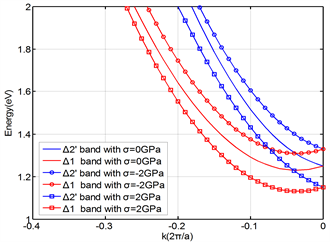
Figure 1. Energy band structure of energy valleys in conduction band under stress in different orientations (a) [±100] energy valley under stress in the [100] orientation (b) [00±1] energy valley under stress in the [100] orientation (c) [±100] energy valley under stress in the [111] orientation (d) [±100] energy valley under stress in the orientation.
compressive stress. The position of the wave vector k corresponding to the minimum energy level of the conduction band does not change, since the shear strain tensor of the [100] crystal orientation is 0 (θ = 0). The minimum value of the Δ1 band in the [00±1] valley is −k0, and the minimum value of band Δ2’ is k0. There is no coupling between the two at point X, the non-diagonal element in Equation (3)
,
and the Δ1 and Δ2’ bands are coincident and the minimum of the energy band is still at point X. Similarly, the change of energy band in [0±10] valley has the same trend as the [00±1] valley. Figure 1(c), Figure 1(d) are the energy spectra under stress in the [111] orientation and the energy band of the [00±1] energy valley under stress in the [111] orientation and the orientation, respectively. It can be seen that the band curvature changes.
In order to reflect the effect of shear stress on the band structure, the [00±1] energy valley is used to calculate under the application of stress in the [110] orientation. As shown in Figure 2(a), the curvature of the energy band changes greatly under the action of uniaxial stress along the [110] crystal orientation, as does the effective mass of electrons. Figure 2(b) shows the band curves of the [±100] and [0±10] valleys along the [110] direction. The figure shows that under the action of uniaxial stress, the energy bands of [±100] and [0±10] are identical, and the Δ1 and Δ2’ bands in [±100] and [0±10] are still degenerate at the point X. The band curvature does not show apparent change.
3.2. Band Edge Level of Conduction Band
The band edge level of the silicon conduction band is a necessary parameter for calculating the density-of-state (DOS) effective mass and conductivity effective mass of electrons. Under the action of uniaxial stress, the degenerate energy level in the conduction band is split, and the movement ΔEC,v of each energy level can be described by deformation potential theory. For each valley, the wave vector kmin corresponding to the valley minimum is substituted into Equation (1), obtaining the band edge level corresponding to each energy valley. For bands with an energy minimum at point X, the band edge level under uniaxial stress can be reduced to
.
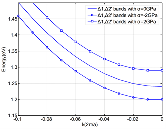
Figure 3 shows the change of band edge energy corresponding to the minimum energy of the conduction band, with respect to the change of uniaxial stress in the [100] orientation. The figure shows that the bottom energy of the band changes with stress, and the degeneracy of the valley is eliminated. Regardless of tensile or compressive stress, the bottom energy valley of the conduction band can be split into a group of valleys in 4-degree degeneracy and a group of valleys in 2-degree degeneracy. Under the action of tensile stress, the minimum of the conduction bands [0±10] and [00±1] can be the band edge. Under compressive stress, however, the minimum of the conduction band [±100] can be the band edge. Compared with the case of no stress, the minimum energy of the conduction band is reduced under the action of both uniaxial compressive and tensile stress. With uniaxial stress in the [110] orientation, the change of band edge level with respect to stress is shown in Figure 3. Unlike the case of stress induced in the [100] orientation, the minimum value of the [00±1] energy valley at the 2-degree degenerate state under tensile stress is the conduction band edge, while under compressive stress, the band edge is the minimum of the [±100] and [0±10] energy valleys which are 4-degree degenerate. Compared with the case of no stress, the minimum energy of the conduction band under uniaxial stress in the [110] orientation increases under compressive stress and decreases under tensile stress.
 (a)
(a)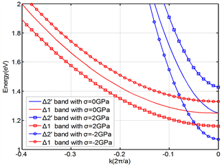 (b)
(b)
Figure 2. Energy band structure of energy valley in conduction band under stress in the [110] orientation. (a) [00±1] energy valley (b) [±100]/[0±10] energy valley.

Figure 3. Band edge of conduction band under stress in the [100] and [110] orientations.
In order to illustrate the relationship between stress and the splitting energy of the conduction band, Figure 4 shows the curve of the conduction band with respect to stress under uniaxial stress in the [100] and [110] orientations. The figure shows that, under the same amount of stress, the uniaxial stress along the [100] orientation has a greater splitting effect than that in the [110] orientation. Therefore, the inhibition effect of uniaxial stress on the inter-band scatter in the [100] orientation is greater than that in the [110] orientation. In addition, Figure 4 also shows the use of the first principle method to calculate the splitting energy of the conduction band with respect to strain changes. The figure shows that the calculated results from this paper are in good agreement with the numerical results from first principle method.
3.3. Effective Mass
Figure 5 compares the two-band k∙p theoretical model and the empirical pseudo-potential method (EPM) [15] in calculating the effective mass of the [00±1]
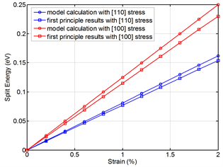
Figure 4. Splitting energy of conduction band under stress in the [100] and [110] orientations.
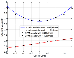
Figure 5. Effective mass of [00±1] energy valley under stress in the [110] orientation.
valley in the silicon conduction band along with the [110] and [001] orientations under stress in the [110] orientation. It shows that the values of electron effective mass in the [001] and [110] orientations calculated by these two methods are generally the same. In the case of compressive stress, the electron effective mass of the [110] orientation calculated from the EPM method is slightly smaller than from the k∙p method.
In the design of scaled CMOS devices, stresses in the [100] and [110] orientations on the (001) plane are mainly used. In this case, the conduction band can be divided into valleys with 2-degree degeneracy and valleys with 4-degree degeneracy. The density-of-state effective mass can be calculated according to Equation (11). Figure 6(a) shows the change of the DOS effective mass under stress in the [100] and [110] orientations, respectively. The figure shows that, under the uniaxial stress in the [100] and [110] orientations, the DOS effective mass of electrons decreases significantly with the increase of stress when stress is small, and then gradually increases to a constant with increasing stress.
 (a)
(a)  (b)
(b)
Figure 6. (a) Density-of-state effective mass and (b) conductivity effective mass under stress in the [100] and [110] orientations.
The change of conductivity effective mass of electrons under stress in the [100] and [110] orientations is shown in Figure 6(b). Under the action of stress in the [100] orientation, the conductivity effective mass increases with the increase of compressive stress, and decreases with the increase of tensile stress. When σ > 1 GPa, the conductivity effective mass change is small. The reason why the effective mass of the conductivity varies with the stress is mainly due to the division of the degenerate energy valleys in the conduction band under stress, which changes the distribution of electrons in the valley. Under the action of uniaxial tensile stress in the [110] orientation, the conductivity effective mass decreases slightly with the increase of stress, while under compressive stress the conductivity effective mass increases slightly with the increase of stress.
For general application, Figure 7(a) and Figure 7(b) show the relationship between density-of-state effective mass and stress, and orientation in the two special crystal planes, for the purpose of providing guidance in choosing the appropriate orientation in device design. The figure shows that the density-of-state effective mass of the conduction band has obvious anisotropy. On the (101) plane, the density-of-state effective mass decreases with the increase of the uniaxial stress, with its minimum value in the [111] orientation. However, for the (111) crystal plane, the change of effective mass is significantly different from that of the (101) crystal plane. In the [0, p/4] and [p/4, p/2] intervals, the DOS effective mass decreases with the increase of the uniaxial tension/compressive stress. When θ = p/4, there is no obvious change. Under certain tensile/compressive stress, the DOS effective mass continuously increases in the range of [0, p/4], but continuously decreases in the range of [p/4, p/2]. DOS effective mass reaches the maximum value at θ = p/4. In addition, the effect of tensile stress and compressive stress on the DOS effective mass shows similar symmetry to what was shown on the energy band of the conduction band. Figure 7(c), Figure 7(d) also give the relationship between conductivity effective mass, stress and orientation for the (101) and (111) crystal planes.
 (a)
(a)  (b)
(b)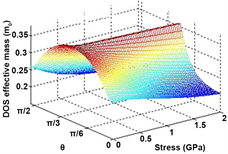 (c)
(c)  (d)
(d)
Figure 7. Density-of-state (DOS) effective mass and conductivity effective mass. (a) (101) plane, (b) (111) plane, (c) (101) plane, (d) (111) plane.
4. Summary
Based on the two-band k∙p theory, the analytical model of energy-dispersion relationship of different energy valleys under arbitrary uniaxial stress on arbitrary crystal plane was established. In this process, the coupling effect between the Δ1 band and the Δ2’ band on the dispersion of different valleys and the variation of valley minimum by shear stress under different uniaxial stresses were considered through the transformation of stress and lattice coordinate systems. Based on the established dispersion relationship on the conduction band, three typical high-symmetry crystal planes (001), (101) and (111) were taken as examples, and major energy structure parameters such as the band edge level, splitting energy, density-of-state (DOS) effective mass, conductivity effective mass, and mobility in the [110] orientation were further calculated. The effective mass values calculated in this work were in good agreement with the values obtained by different methods, which confirmed the validity of this model. In addition, the relationship of DOS effective mass and conductivity effective mass with stress and orientation for the (101) and (111) planes was also given.
In addition to the above mentioned, in fact, strain technology can be involved not only in MOS devices, but also in bipolar and optoelectronic devices. Recent studies of TCAD simulation pointed out that the strain effect has an influence on the electrical parameters of bipolar transistors, it is possible to introduce uniaxial stress induced by the functional oxides into silicon photonics applications. The proposed band-parameter model and calculation results can provide a theoretical reference for the design and optimization for silicon-based nano-electronic devices, bipolar devices or optoeletronic devices, and TCAD simulation.
Acknowledgements
This work is financially supported by National Natural Science Foundation of China (Grant Nos.: 61404019, 61704147), the Science Fund from the Education Department of Hebei Province, China (Grant No.: QN2017150).
Cite this paper
Wang, G.Y., Yu, M.D. and Zhou, C.Y. (2018) Modelling and Calculation of Silicon Conduction Band Structure and Parameters with Arbitrary Uniaxial Stress. Journal of Applied Mathematics and Physics, 6, 183-197. https://doi.org/10.4236/jamp.2018.61018
References
- 1. Sun, W.K. and Shin, H.S. (2014) Optimization of Uniaxial Stress for High Electron Mobility on Biaxially-Straned n-MOSFETs. Solid-State Electronics, 94, 23-27. https://doi.org/10.1016/j.sse.2014.01.005
- 2. Zhou, X., Chandrasekaran, K., Chiah, S.B., et al. (2006) Implicit Analytical Surface/Interface Potential Solutions for Modeling Strained-Si MOSFETs. IEEE Transactions on Electron Devices, 12, 3110-3117.
- 3. Sun, G.D., Zhang M., Xue Z.Y., et al. (2014) Strain Redistribution in Free-Standing Bridge Structure Released from Strained Silicon-on-Insulator. Applied Physics Letters, 105, 193505. https://doi.org/10.1063/1.4901820
- 4. Gupta, S., Moroz, V., Smith, L., et al. (2014) 7-nm FinFET CMOS Design Enabled by Stress Engineering Using Si, Ge, and Sn. IEEE Transactions on Electron Devices, 61, 1222-1230. https://doi.org/10.1109/TED.2014.2311129
- 5. Vogel, D., Auerswald, E., Auersperg, J., et al. (2014) Stress Analyses of High Spatial Resolution on TSV and BEoL Structures. Microelectronics Reliability, 54, 1963-1968. https://doi.org/10.1016/j.microrel.2014.07.098
- 6. Biswas, A., Luong, G.V., et al. (2017) Benchmarking of Homojunction Strained-Si NW Tunnel FETs for Basic Analog Functions. IEEE Transactions on Electron Devices, 64, 1441-1448. https://doi.org/10.1109/TED.2017.2665527
- 7. Sun, Y., Thompson, S.E. and Nishida, T. (2007) Physics of Strain Effects in Semiconductors and Metal-Oxide-Semiconductor Field-Effect Transistors. Joural of Applied Physics, 101, 104503. https://doi.org/10.1063/1.2730561
- 8. Fischetti, M.V. and Laux, S.E. (1996) Full-Band Monte Carlo Simulation of High-Energy Transport and Impact Ionization of Electrons and Holes in Ge, Si, and GaAs. Solid State Device Research Conference, Tokyo, 813-820.
- 9. Rieger, M.M. and Vogl, P. (1993) Electrionic-Band Parameters in Strained Si1-xGex Alloys on Si1-yGey Substrates. Physical Review B, 48, 14276. https://doi.org/10.1103/PhysRevB.48.14276
- 10. Sverdlov, V., Karlowatz, G., Dhar, S., et al. (2008) Two-Band kp Model for the Conduction Band in Silicon: Impact of Strain and Confinement on Band Structure and Mobility. Solid-State Electronics, 52, 1563-1568. https://doi.org/10.1016/j.sse.2008.06.019
- 11. Sverdlov, V. and Selberherr, S. (2008) Electron Subband Structrue and Controlled Valley Splitting in Silicon Thin-Body SOI FETs: Two-Band kp Theory and Beyond. Solid-State Electronics, 52, 1861-1866. https://doi.org/10.1016/j.sse.2008.06.054
- 12. Dhar, S., Ungersbock, E., Kosina, H., et al. (2007) Electron Mobility Model for <110> Stressed Silicon Including Strain-Dependent Mass. IEEE Transactions on Nanotechnology, 6, 97-100. https://doi.org/10.1109/TNANO.2006.888533
- 13. Hensel, J.C., Hasegawa, H. and Nakayama, A.M. (1965) Cyclotron Resonance in Uniaixally Stressed Silicon. II. Nature of the Covalent Bond. Physical Review, 138, A225. https://doi.org/10.1103/PhysRev.138.A225
- 14. Tan, Y.H., Li, X.J., Tian, L.L., et al. (2008) Analytical Electron-Mobility Model for Arbitrarily Stressed Silicon. IEEE Transactions on Electron Devices, 55, 1386-1390. https://doi.org/10.1109/TED.2008.921074
- 15. Ungersbock, E., Gos, W., Dhar, S., et al. (2008) The Effect of Uniaxial Stress on Band Structure and Electron Mobility of Silicon. Mathematics and Computers in Simulation, 4, 1071-1077. https://doi.org/10.1016/j.matcom.2007.10.004