Optics and Photonics Journal
Vol.3 No.1(2013), Article ID:29033,10 pages DOI:10.4236/opj.2013.31017
The Design and Manufacturing of Diffraction Optical Elements to Form a Dot-Composed Etalon Image within the Optical Systems
Bauman Moscow State Technical University (BMSTU), Moscow, Russia
Email: h_sagatelyan@mail.ru
Received December 27, 2012; revised January 28, 2013; accepted February 5, 2013
Keywords: Optical Glass; Plasma-Chemical Etching; Selectivity; Diffraction Gratings; Micro-Optics
ABSTRACT
The possibilities of manufacturing of diffraction optical elements (DOE), using the “Caroline 15 PE” plasma-etching machine were considered. It is established that at thickness of chromic mask of 100 nm the plasma-chemical etching (PCE) method reaches depth of surface micro-profile to 1.4 μm on optical glass. It allows increasing the diffraction efficiency of DOE to 0.3 - 0.35 on the second order of diffraction.
1. Introduction
The development of optical subsystems, having minimal weight and size characteristics, but ensuring the reference-class location of several points in the plane of the image on a CCD-matrix (Figure 1), is an actual problem for a number of optical devices [1]. The most effective way to solve this problem is to use the diffractive optical element (DOE), which works on the transmission of light mode and contains several diffraction gratings (Figure 2) —one for each of points, formed by it.
The principle of operation of to be designed DOE is shown on the Figure 3. The set of parallel laser beams is falling on the DOE with angle of light incidence α. To minimize the size characteristic of optical device, it is necessary to provide as big as possible value of angle of incidence α. As it can be seen out of Figure 3, the DOE has to work on not zero order of the spectrum. So, the diffraction gratings of DOE are transferring echeletts— phase diffraction gratins, which have an ability to concentrate the diffracted light in the spectrum of defined (not zero) order.
At the present time only the echeletts, working on reflection of light and fabricated by engraving the pattern with a triangle micro profile, which creates an additional difference of travel in the limits of each period of grating [2], on the surface of the metal by especial cutting tool, are known. As far as the DOE, which has to be created, must work in transition mode, being made of optical inorganic glass, the cutting out of desired profile on its working surface is impossible. This kind of micro-optics workpieces can be created on basis of implementing the method of plasma chemical etching (PCE) [3].
The plasma-chemical etching method has a number of destinations, which allow forming on the worked surface narrow (width lower than 1 micrometer) gaps with relatively large (1 - 2 micrometer) deepness. The shortcoming of plasma-chemical etching consists in the fact, that by this method, from a practical point of view, it is possible to build only the binary micro-relief.
However, in the case of tilted fall of light on the diffraction grating [4], the binary rectangular micro-relief of the phase grating turns into a saw-like one (Figure 4). This allows one to create an echelett, manufactured by the method of plasma-chemical etching.
The object of this work was to create a transmitting DOE working on the 2nd order of diffraction. To achieve this goal the following tasks were solved:
• Theoretical determination of the required depth of grooves of phase diffraction gratings of DOE;
• Fabrication of DOE of optical glass by the PCE method including: 1) choice of technological equipment; 2) carrying out of experimental research on PCE of optical glass; 3) selection of optimal mode of PCE operation; 4) optical verification of fabricated DOEs;
• Discussion of acquired results of experimental research to explain the main regularities and peculiarities of PCE of optical glass.
The novelty of our works consist in establishment of interconnection between the conditions of PCE on manufacturing the DOE with it’s operational behavior.
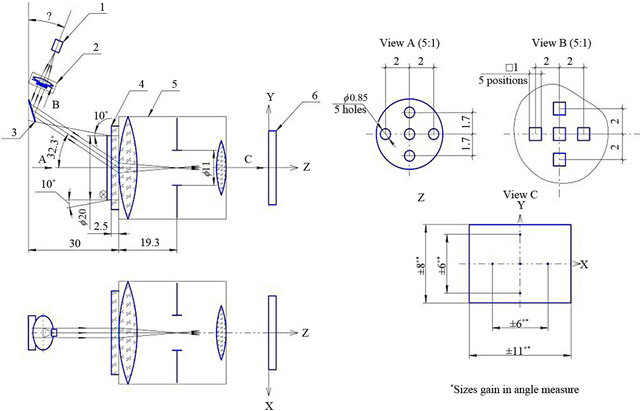
Figure 1. The optical scheme of device.
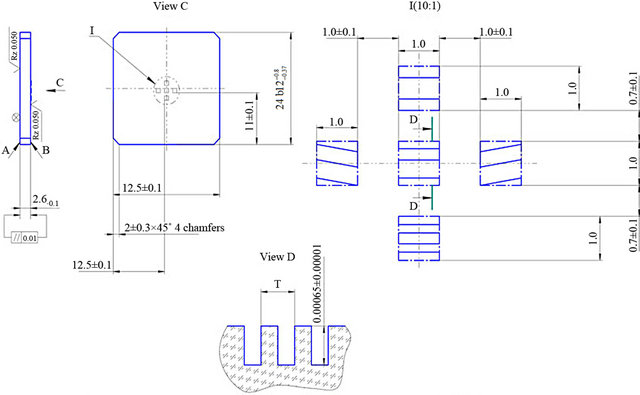
Figure 2. The design of DOE.

Figure 3. The scheme of DOE work: 1—Incident parallel beams; 2—Diffracted beams; 3—Diffraction gratings; 4—DOE.
 (a)
(a) (b)
(b)
Figure 4. The scheme of manufacture of DOE, working as an transmitting echelett (1 and 2—the incident and the diffracted beams): (a) Creating of mask; (b) Plasma-chemical etching; (c) The incidence of beam on the phase grating; (d) The equivalent echelett.
2. Theoretical Justification
It is known [5], that for the concentration of energy in a given direction two conditions must be met, which, with regard to the case under consideration, can be formulated in the following way:
1) The direction of the zero order from a separate refracting element should coincide with the direction on the maximum of the required direction from the grating as a whole;
2) The direction on the zero order spectrum from the grating as a whole should coincide with the direction of the minimum while diffracting on the separate refracting element.
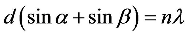
For the analysis of the first conditions we can write down the equation of the diffraction grating
 , (1)
, (1)
where d is the period of the diffraction grating; α—the incidence angle; β—the angle of required diffraction order; n—the number of order; λ—the wave length.
We shall consider the incidence of beam on the central diffraction grating of DOE (see Figure 1). Here we have β = 0 (the perpendicularity to the working plane of the DOE of the required direction on diffraction maximum). To work on the second order of diffraction (n = 2), expression (1) can be written in the form of
 . (2)
. (2)
The expression (2) specifies an unambiguous relationship between the required angle of incidence α and the period d of the diffraction grating. So, for α = 30˚ the period of the diffraction grating should be d = 2.6 μm.
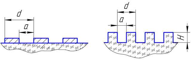
Continuing to analyze the first condition for the energy concentration by an echelett, we can set the regularities of the formation of emission of zero order from a separate refracting element. It is obvious that in this case we have the irradiation, diffracted on the phase grating with a rectangular profile (Figure 5(a)).
The relative spectral intensity of radiation I0 for the zero order in this case is described by expression [6]
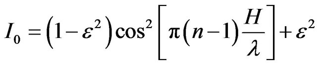 , (3)
, (3)
where:  is the asymmetry factor of rectangular phase grating; n is the refractive index of glass.
The plot of I0(H) dependence for n = 1.5; λ = 0.65 μm and ε = 0 is shown on Figure 5, d. It follows from this plot, that the maximum of relative spectral efficiency at the zero order of diffraction can be achieved at H = 1.3 μm. Thereby, the required H depth of grooves of the rectangular profile, which are formed by means of plasmachemical etching (see Figure 4(b)), must be determined by the following formula, driven out from the expression (3):
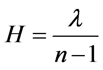 , (4)
, (4)
Let us consider the second condition for concentration of energy by the echelett, which in this case boils down to the fact, that toward the direction of ray 1 (see Figure 4(d)) there will be located the minimum of intensity of radiation, which is diffracted on the separate element. An appropriate model for the presented on the Figure 4(d) equivalent scheme is describing the echelett by a phase grating with a triangular profile (Figure 5(b)). Comparing Figures 4(d) and 5(c), we can assume that the deepness Δ of triangular relief of such a phase grating works out as
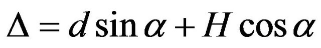 . (5)
. (5)
The minimum of intensity of radiation for the zero order of diffraction on a separate element of profile determines from the following expression [6]:
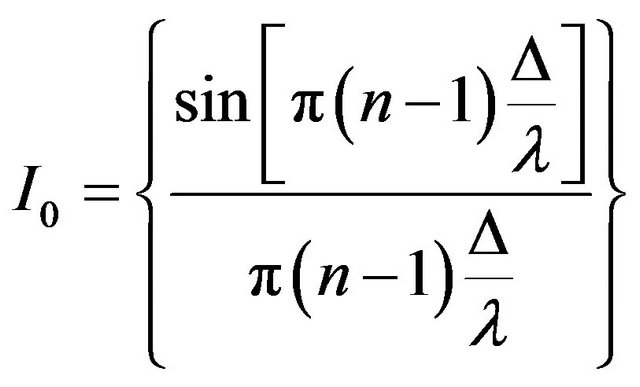 , (6)
, (6)
where Δ is the deepness of relief (Figure 5(c)), calculated by formula (5).
The plot of I0(H) dependence for n = 1.5; λ = 0.65 μm; α = 30˚ and d = 3 μm is shown on Figure 5(e). In this case, as well, as in previous one, we can see, that intensity of radiation of zero order of diffraction on the separate element of profile achieves its minimum at deepness of etching (see Figure 4(b)) H = 1.3 μm.
Coincidence of required deepness of etching H = 1.3 μm to maximize the intensity of radiation in the required direction of diffraction (see Figure 5(b)) as well as to minimize the intensity of radiation in the direction of zero order for the grating as a whole (see Figure 5(e)), indicates that the light transmitting echelett, designed to work on the second order of spectrum, can be produced by the method of plasma-chemical etching.
3. Experimental
The most appropriate way to create plasma, which is a source of positively charged ions and chemically active radicals, ensuring the removal of the processed material during the PCE of optical glass—an inorganic dielectric
 (a)
(a)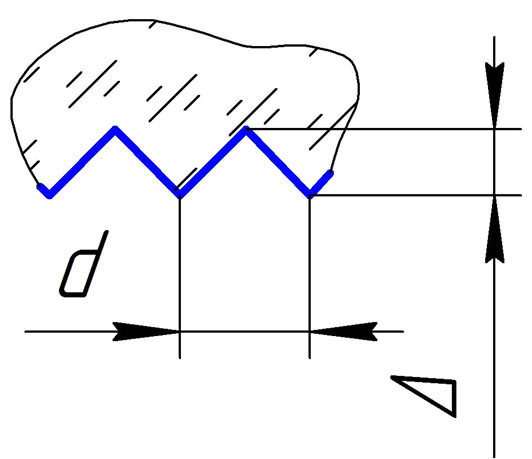 (b)
(b)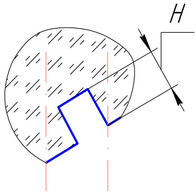 (c)
(c)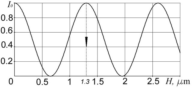 (d)
(d)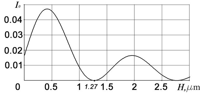 (e)
(e)
Figure 5. Phase diffraction gratings with a rectangular (a), a triangular (b) and an equivalent (c) profile as well as respective (d, e) relative spectral intensities of zero order.
material—is application of high-frequency inductive discharge. Such a discharge allows adjusting the power supply and, consequently, the temperature of plasma in a wide range, providing at the same time the sufficient number of free electrons to compensate the positive charge, which accumulates on the dielectric processed work-piece.
3.1. The Choice of Technological Equipment for Plasma-Chemical Etching (PCE) of Optical Glass
Experimental research of electro-physical characteristics of such facilities [7] allowed establishing a number of regularities of generation of currents (ion, electron) and voltages (in particular, the bias voltage) in the working chamber. However, these studies do not allow establishing any direct analytical relationships between the electro-physical parameters of the device and the output parameters of the PCE process, such, for example, as the deepness of micro-relief on the formed functional surface of DOE.
As the equipment to realize PCE process with regard to the manufacturing of DOE, the “Caroline 15 PE” device for plasma-chemical etching [8] was chosen, which is used in microelectronics to produce integrated circuits on the wafers having 200 mm diameter. The features of constructive arrangement of this device are presented on Figure 6.
While choosing of this device as an equipment to design the technology to produce DOE, made of optical glass (the main component of the composition of the furnace charge to melting such a glass is silicon dioxide), the information about a positive results of its using to produce parts, made of single-crystal quartz [9], was taken into consideration. Some results of experimental research of applying the “Caroline 15 PE” device to etching the single-crystal quartz at great depths—more than 200 μm —are presented in [9] without a detailed description of
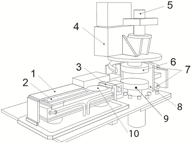
Figure 6. The “Caroline 15 PE” device for plasma-chemical etching: 1—sluice chamber; 2—transfer arm; 3—slit shutter; 4—impedance matcher; 5—laser control system; 6— antenna; 7—electromagnetic system; 8—housing of the working chamber; 9—wafer holding table; 10—carrier.
conditions and regimes of PCE operation. Particularly, the material of mask, the method of its gaining and the thickness, necessary to etch on depresses of order of tens of micrometers are not disclosed.
The results of our preliminary experimental studies on applying the “Caroline 15 PE” device to PCE of optical glass, using chrome and iron oxide as materials of the mask and blanks of reticles as crude product for DOE, are presented in [10].
3.2. Experimental Studies on Making Phase DOEs
Crude products (work-pieces) of DOE, having 35 mm in diameter, were gained by drilling out of blanks of reticles, used in integrated circuit technology. So, the material of phase DOE was the glass, used to make reticles. For the placement of DOE work-pieces having diameter 35 mm, on the wafer holding table of “Caroline 15 PE” device, which is intended to 200 mm silicon wafers, the special shielding carrier was designed.
The results of experimental studies of PHE operation for DOE manufacturing are shown below.
The influence of etching time t on the attained deepness of grooves of diffraction gratings while providing the PCE operation for phase DOE with chrome mask was investigated.
The following etching regime was fixed on “Caroline 15 PE” device: etching gas consumption (chlorofluorocarbon CF4—Freon)—CCF4 = 2.4 l/min; plasma gas (argon) flow CAr = 0.8 l/min; table cooling gas (helium) consumption—CHe = 1.2 l/min; superposed magnetization current in coils, which embrace the chamber with plasma—I = 2.0 A; the power feed to the antenna—Pа = 250 W; the power feed to the table—Pст = 250 W; rotating velocity n of the rotor of turbo—molecular pump— 100% of nominal.
During the work of “Caroline 15 PE” device plasmachemical etching conditions, which are associated with the functioning of two high-frequency generators with their impedance matchers, loading respectively at the antenna and the table, are formed in the process itself. These conditions include: the actual powers at the antenna and table, in both cases the values of powers of incent and reflected waves are registered at that; the bias voltage at the table U; the pressure in the working chamber p.
The resulting graphs of influence of PCE process duration on the deepness of grooving of diffraction gratings, obtained on the basis of research, carried out on the Surfcoder SE 1700 α by Kosaka Laboratory Ltd./Japan surface roughness measuring instrument, are presented on Figure 7. The deepness of profile was determined on two fabrication stages: 1) after the realization of PCE

Figure 7. The dependences of diffraction grating’s grooves deepness H on duration t of plasma-chemical etching (PCE) operation, gained after the PCE operation (curve 1) and after the operation of liquid acid etching, following the PCE operation (curve 2).
operation itself; 2) after the operation of acid etching, which was carried out to remove the remnants of chrome mask. On Figure 7 the plot of dependence of diffractive grating’s grooves, measured after the PCE operation itself corresponds to the broken curve 1, and the broken curve 2 corresponds to plot of dependence of diffraction grating’s grooves depresses, obtained after the executing of acid etching operation, following the PCE operation on the same samples. Considering the curves 1 and 2 on the Figure 7, one can see the following regularities and peculiarities of the character of influence of the duration of PCE operation on the formed depth of diffraction grating’s groove.
1) Both curves 1 and 2 on Figure 2 have a maximum of grooves’ depth on the PHE process duration topt = 30 min. In other words on t < topt PCE process durations the deepness of grooves of diffractive gratings increases with the increase of PCE process duration, and on the PCE process durations t > topt the deepness of grooves of diffractive gratings decreases with the increase of PCE process duration.
2) Curves 1 and 2 intersect on the PCE process duration tcr = 22 min. On the t < tcr durations of PCE process, the deepness of grooves of diffractive gratings, measured after the PCE operation, exceeds the deepness of the same grooves, measured after the operation of acid etching, and on the t > tcr durations of PHE process the deepness of grooves of diffraction gratings, measured after the PHE operation, occur to be less than deepness of same grooving, measured after the operation of acid etching. In other words, in the latter case the acid etching operation leads to an increase in diffraction grating grooving’s depth.
At t = tcr moment the deepness of grooves of diffraction gratings doesn’t change after the execution of acid etching operation.
3) For the t > tcr PCE process durations the difference between the deepness of grooves after the PCE and after the acid etching increases with the raise of the PCE process’s duration.
The analysis of the results of research of influence of duration of the PCE operation on the depth of relief of phase diffraction grating, presented on Figure 7, allows one to contend, that for the achievement of maximal glass etching deepness the single determining parameter is the selectivity of etching of glass related to material of mask. The operation of PCE of optical glass must be carried out on the most reasonable (optimal) mode. The optimum is the mode, which provides the maximum of the selectivity of etching. In this case, the ratio of etching speeds of the glass and the mask is understood as the selectivity of etching.
To find out the optimal mode of PCE, the series of experiments was carried out, using the iron oxide as the material of mask. The samples for these investigations were drilled out of ready to use reticles, used on integrated circuits’ production. The mask for the PCE operation corresponded to not transparent areas of reticle.
The influence of relation of consumptions of the plasma generating (argon) and reactive (Freon) gases on a number of output parameters of PCE process was investigated. The result of mentioned series of experiments is presented on the Figure 8 as a number of graphs. This dependences are acquired on fixing of other conditions of the process (the powers on antenna and the table, magnetization current, helium consumption, the speed of turbo-molecular pump) on the same levels, as at the previous experimental studies, results of which are presented on Figure 7.
Considering the graphs on Figure 8, one can see, that dependences of parameter of our interest—the selectivity r of etching—on consumptions of both argon and Freon, possess pronounced extremum nature, i.e. they’ve got maximums. We can assume that the optimal mode of PCE of glass on the “Caroline 15 PE” device is established—it corresponds to the consumption of argon CAr = 0.8 l/min at simultaneous consumption of Freon CCF4 = 2.4 l/min.
Practical application of plasma-chemical etching operation is conditioned on necessity to produce exactly phase diffraction gratings, which as opposed to ordinary

Figure 8. The dependences of productivity q and selectivity r of etching, as well as bias voltage Ud and vacuum pressure p in the chamber on consumptions f of argon (Ar) and Freon (CF4).
(amplitude) ones provide heightened diffraction efficiency. The experimental study of diffraction efficiency of diffraction gratings of DOE with different deepness of grooves, fabricated with use of PCE method, was carried out on the specially designed optical stand.
The intensities of beams of 0. 1st, 2nd, 3d and −1st (“minus first”) orders were measured with the help of special measuring instrument on tilted incidence of light. For amplitude diffraction gratings the diffraction efficiency decreases to the greatest extent on transition to the second and higher orders of diffraction. So, the most relevant is the question of determining the optimal deepness of diffraction gratings, providing the maximum of energy in the second order of diffraction.
Acquired dependencies of diffraction efficiency as the portion of the light’s intensity of beam of the 2nd order of diffraction in the summarized intensity of light, transferred the DOE, on the deepness d of grooves of diffraction gratings with different periods are presented on the Figure 9, considering which one can see, that the partial share of second order of diffraction can reach and even exceed 30%.
Empirically established dependencies, which are presented as graphs on Figure 9, also indicate, that to the heighten the diffraction efficiency of phase diffraction gratings the deepness of grooves must be increased as much as possible.
4. Discussion
The heightening of diffraction efficiency of phase diffraction gratings in the 2nd order of diffraction with increasing of deepness of grooving of diffraction grating (see Figure 9) can be explained by decreasing of relative spectral intensity of radiation for the zero order of diffraction [11]. Generally speaking, in accordance with the theory of light diffraction on phase diffraction gratings with ideal rectangular profile of micro-relief, the relative spectral intensity of zero order of diffraction should be changed in waves, achieving the maximum (for our conditions) at grooving depths 700 nm, 1400 nm and etc. In practice, however, the obtained form of micro-relief of diffraction grating differs of ideal rectangular, so far as rounding occurs on the edges of ledges and the walls of micro-relief aren’t upright, but are tilted on angle up to 30˚ to vertical line.
Thereby, the nominally rectangular shape of micro-relief of phase diffraction gratings in practice is close to the triangle, and for such a form of micro-relief, in accordance with the theory of diffraction [6], the relative spectral intensity of zero order of diffraction with increasing of depth of grooving of diffraction grating is changing wavy, but nevertheless tends to zero. Therefore, to raise the diffraction efficiency of phase diffraction gratings, the depth of grooving must be increased as possible.
As has already been noted above, maximally achieving by PCE deepness of diffraction grating’s grooving determines mainly by the selectivity of etching of optical glass related to material of mask.
In connection with this, the detected maximums in r = f(CAr) and r = f(CCF4) dependencies (see Figure 8) are
 (a)
(a)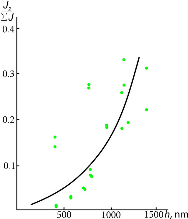 (b)
(b)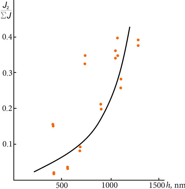 (c)
(c)
Figure 9. The dependences of ratio of light’s intensity in the beam of 2nd order of diffraction I2 to sum of intensities of light in the beams of 0, 1st, 2nd, 3rd and −1st orders of diffraction on the deepness h of grooves of diffraction gratings with the period d = 2 μm (a); d = 2.5 μm (b) and d = 3 μm (c).
gaining an exceptional importance. The graphs of other dependencies, presented at the same drawing, help to explain these maximums.
Among these graphs the most easily explainable are graphs of razing of vacuum pressure p with increasing of consumptions of argon and Freon. Explaining the characters of other dependencies is complicated and that is connected with the fundamental differences in the physical essence of the process, concomitant with the presence of atoms of argon and molecules of Freon in plasma. Whereas atoms of argon in high frequency plasma are dissociating on positively charged ions and electrons, the molecules of Freon in the same plasma are acquiring only the not-coupled electrons, becoming radicals (though formation of free electrons and complicated positively and negatively charged ions is possible as well).
Naturally, the rising of argon consumption leads to increasing of density of electrons in plasma, which causes decreasing of bias voltage Ud on the table, as well as to increasing of ion current through the work-piece of DOE under treatment, which results increasing of productivity q of glass etching. Existence of a minimum in the dependence of productivity of etching on argon consumption is explained by decreasing of the length of the free run of argon ions in the accelerating electric field with increasing of density of plasma: on heighted concentration of argon the physical destruction of glass with ions of argon is prevailed, and this is accompanied also by intensification of destruction of mask material and by decreasing of selectivity r of etching; on lowered concentration of argon it’s ions are being successful to gain in the accelerating electric field an energy, which is enough to intensify the physical destruction of worked surface of glass (increasing of etching productivity q) as well as destruction of mask, which also brings to decreasing of etching selectivity r.
The disclosed regularities and features of the relationship of achievable etching depth of optical glass with the duration of PCE process could be explained as follows.
1) At the t = topt moment (see Figure 7) an almost complete removal of chromium mask occurs—on areas, protected by the mask, only the separate, not connected with each other parts of mask can remain in form of isles. If the direction of the vector of speed of all the ions and radicals of plasma would be exceptionally on vertical line (perpendicular to treated surface), then, beginning of this moment, the changing of deepness of grooves should not occur. However, as far as for the realized conditions of PCE, other directions of vectors of speeds of ions and radicals (active particles) are as well typical, so the peaks of micro-profile of phase diffraction grating are worked out more intensively. The bottom of the micro-profile of diffraction grating is reach by not all of the particles, which could be there in case of the vertical flux, but the top points of micro-profile are reached by all of the particles, flying on them in the vertical flow, and by some of the particles, which are flying in tilted direction. Because of the more intense working out of peaks of micro-profile, the deepness of grooves decreases with increasing of etching time when t > topt.
Thereby, we can assume that the maximum of selectivity of etching of glass r is observing on the minimization of the etching rates q. On this, to reach the required depth of grooving it is necessary to increase the duration of PCE process, taking into account the fact that the dependence of achievable depth of etching on etching duration has a complicated character (see Figure 7).
2) The PCE process is characterized not only by removal of treating materials (glass and chromium), but as well—by the growth of some film on the processed surfaces (this effect in the practice of plasma-chemical processes is named as “the drop-off”). In accordance with the existing concepts, the growing film is a polymer—the fluoroplastic (because of it, the mentioned stray process carries as well a more exact name—“the polymerization”), which is created of Freon. The removal of worked materials happens from under the growing film of the polymer. The film grows both on chromium and glass and the rate of growth of the film on the chromium can be higher or lower than the rate of growth of the film on the glass. Simultaneously, the rate of etching of glass is much higher than the rate of chromium etching. At the moment of t = tcr it occurs, that the thickness of the film on the glass is equal exactly to the sum of two thicknesses—the thickness of remaining chromium layer and the thickness of the film, which had been grown on the chromium. Because of this, after the acid etching the deepness of grooves of diffraction grating doesn’t change. Until t < tcr the thickness of remaining layer of chromium in the sum with the thickness of the polymer film, grown on it, exceed the thickness of polymer film, grown on the glass. So, as a result of acid etching, the deepness of grooves of diffraction grating decreases. If t > tcr, then the thickness of polymer film, which is grown on the glass, exceeds the total thickness of remaining layer of chromium and the film, which is grown on chromium. This leads to increasing of depth of the diffraction grating’s grooving after the execution of acid etching operation.
3) With the increase of the duration of PCE operation the thickness of film, that is dropped-off on the treated surface of glass as a result of spurious reaction of Freon polymerization, increases monotonically, asymptotically approaching the some limit value, consistent to the equality of rates of growing end etching of this film. If PCE operation is excessively long, i.e. such, in which the protecting Chromium mask is already removed, and then during the operation of acid etching, which follows the PCE operation, the removal only of mentioned film occurs. Because of that, the difference between the deepness of diffraction grating’s grooving before and after the operation of acid etching monotonically increases with increasing of exceeding duration of PCE operation.
On the basis of analysis and explanation of physical essence of the regularities and peculiarities of PCE process, detected by experimental methods, the following conclusions and recommendations to design the PCE operation in the manufacture of DOE can be formulated.
1) To achieve the estimated depth of grooves of phase diffraction gratings by a method of automatically get the size as well as by the method of trial processes and measurements the correlation between the PCE operation duration t and it’s critical duration tcr must be taken into account. If t < tcr, then as a result of acid etching operation, which follows the PCE operation and has the purpose of removing of remains of mask, the deepness of grooves will decrease, and if t > tcr, then it will increase.
2) It is established, that with increasing of grooving’s depth from 0 until 1.5 μm the diffraction efficiency of phase diffraction grating, manufactured by PCE method, rises monotonically, so to increase the diffraction efficiency the maximum possible deepness of grooving in the specified range should be sought.
3) To achieve the maximal depth of grooving of phase diffraction grating it is necessary to observe the t = topt condition, where topt is the optimal duration of PCE process. With greater or lesser duration of PCE operation the deepness of grooves of phase diffraction grating will be less, than maximally achievable.
4) The complete use of the capabilities, which are assignable by thickness and material of mask, is possible by providing the maximal etching selectivity r of glass relating to mask material by selecting the optimal regime of PCE process.
5. Acknowledgements
This work is executed on carrying out the Research on the State contract N P950 from 27.05.2010 in the framework of Federal target program “Scientific and scientific-pedagogical personnel of innovative Russia” on years 2009-2013.
REFERENCES
- F. Ananasso and I. Bennion, “Optical Technologies for Signal Processing in Satellite Repeaters,” IEEE Communications Magazine, Vol. 28, No. 2, 1990, pp. 55-64. doi:10.1109/35.46686
- E. G. Loewen and E. Popov, “Diffraction Gratings Applications,” Marcel Dekker, Inc., New York, Basel, 1997.
- S. Jensen, “Inductively Coupled Plasma Etching for Microsystems,” MIC, Lyngby, Denmark, 2004.
- T. Zhang, M. Yonemura and Y. Kato, “Optical Design of an Array-Grating Compressor for High Power Laser Pulses,” Fusion Engineering and Design, Vol. 44, No. 1-4, 1999. pp. 127-131.
- Z. Peng, D. A. Fattl, A. Faraou, M. Fiorentino, J. Li and R.G. Beausoleil, “Reflective Silicon Binary Diffraction Grating for Visible Wavelengths” Optics Letters, Vol. 36, No. 8, 2011, pp. 1515-1517. doi:10.1364/OL.36.001515
- W. Friedl and B. Hartenstein, “Energy Distribution of Diffraction Gratings as a Function of Groove Form,” Journal of the Optical Society of America, Vol. 45, No. 5, 1955, pp. 398-399.
- M. Mao, Y. N. Wang and A. Bogaerts, “Numerical Study of the Plasma Chemistry in Inductively Coupled SF6 and SF6/Ar Plasma Used for Deep Silicon Etching Applications,” Journal of Physics D: Applied Physics, Vol. 44, No. 43, 2011, Article ID: 435202. doi:10.1088/0022-3727/44/43/435202
- www.esto-vacuum.ru/oborudovanie/caroline/caroline-rr
- D. A. Zeze, R. D. Forrest, J. P. Cary, D. C. Cox, I. D. Robertson, B. L. Weiss and S. R. P. Silva, “Reactive Ion Etching of Quartz and Pyrex for Microelectronic Applications,” Journal of Applied Physics, Vol. 92, No. 7, 2002, pp. 3824-3829. doi:10.1063/1.1503167
- S. B. Odinokov and G. R. Sagatelyan, “Technology of Manufacturing of Diffraction and Hologram Optical Parts with Functional Microrelief of Surface by Method of Plasma-Chemical Etching,” Vestnik MGTU, Priborostroenie, No. 2, 2010, pp. 92-104.
- K. Knop, “Rigorous Diffraction Theory for Transmission Phase Gratings with Deep Rectangular Grooves,” Journal of Optical Society America A, Vol. 67, No. 9, 1978, pp. 1206-1210. doi:10.1364/JOSAA.9.001206