Circuits and Systems
Vol. 4 No. 2 (2013) , Article ID: 29914 , 8 pages DOI:10.4236/cs.2013.42032
Design and Optimization of Printed Circuit Board Inductors for Wireless Power Transfer System
Department of Electrical Engineering and Computer Science, University of Tennessee, Knoxville, USA
Email: aislam@utk.edu
Copyright © 2013 Ashraf B. Islam et al. This is an open access article distributed under the Creative Commons Attribution License, which permits unrestricted use, distribution, and reproduction in any medium, provided the original work is properly cited.
Received November 20, 2012; revised December 20, 2012; accepted December 27, 2012
Keywords: Inductive Link; Solenoid; PCB; Wireless Power Transfer; Biomedical
ABSTRACT
Wireless power transfer via inductive link is becoming a popular choice as an alternate powering scheme for biomedical sensor electronics. Spiral printed circuit board (PCB) inductors are gaining attractions for wireless power transfer applications due to their various advantages over conventional inductors such as low-cost, batch fabrication, durability, manufacturability on flexible substrates, etc. In this work, design of a multi-spiral stacked solenoidal inductor for biomedical application in 13.56 MHz band is presented. Proposed stacking method enhances the inductance density of the inductor for a given area. This paper reports an optimization technique for design and implementation of the PCB inductors. The proposed scheme shows higher inductance and better figure-of-merit values compared to PCB inductors reported in literature, which are desirable for wireless power transfer system.
1. Introduction
With the advancement of biomedical instrumentation technologies, sensor based remote healthcare monitoring system is gaining increasing attention in the recent years. These sensors can be classified as wearable or implantable. While the wearable sensors are placed outside the body, the implantable types are placed underneath the skin or inside the body cavity typically via surgical means. Implantable sensors are designed to acquire the information on the vital physiological phenomena by monitoring blood glucose level [1-3], lactate in the bloodstream or tissues [4], pH, oxygen, and minimally invasive monitoring of pressure in blood vessels and intracranial compartments, etc. [5]. These sensors include associated electronic circuits for signal processing and data transmission. Powering these circuits is always a crucial design challenge since the batteries are typically not allowed in an implantable system which can come in contact with blood resulting in serious health risks and can be fatal in some cases. An alternate approach is to supply power wirelessly for tether-less and battery-less operation of the circuits. Inductive coupling is the most common method of wireless power transfer (WPT) to the implantable sensors [6-9]. For good inductive coupling, the inductors should have high inductance (L) as well as high quality factor (Q) [10]. But the physical dimensions of the implanted inductors cannot be large due to various biomedical constraints. Therefore, there is a need for small sized and high inductance, high quality factor inductors for implantable sensor applications. Inductors account for more than 90% of the size of the total implantable system and therefore the reduction of the size of the inductor will significantly reduce the area and the volume of the overall system.
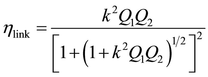
Efficiency of an inductive link in parallel resonance can be described as [11],
 (1)
(1)
where, Q1 and Q2 are the unloaded quality factors of the primary and secondary coils, respectively and “k” is the mutual coupling which has a value ranging from 0 to 1. This equation confirms that the efficiency increases as k2Q1Q2 increases, and therefore the first and the foremost design consideration in an inductive link design is the attainment of the highest possible unloaded Q and k. These two vital parameters are functions of shape, size and relative positions of the coils.
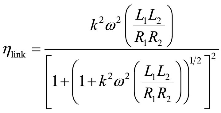
Substituting Q1 = wL1/R1, Q2 = wL2/R2 in the Equation (1) results in,
 (2)
(2)
where ω is the frequency, L1 and L2 are the inductances and R1 and R2 are the resistances of the primary and the secondary coils, respectively. It is evident from this equation that increasing the inductance value of the inductors will increase the efficiency of the overall system. Therefore small sized high inductance coil has two distinctive advantages—high link efficiency and smaller size that increases the feasibility of placing WPT based implantable system in various biomedical applications.
There are various types of inductors designed for various system applications. For example, spiral printed circuit board (PCB) planar inductors are widely used in RF applications. PCBs are inexpensive, low-cost and can be fabricated in large amounts in batches. Their geometries and aspect ratios can be optimized, which make them suitable for implantable systems placed underneath the skin or within the epidural space [12]. PCBs fabricated on thin flexible substrates can also comply with body curvatures. For example, Shah et al. proposed PCBs for neuroprosthetic transcranial telemetry applications [13]. Micromachining techniques have also been proposed for fabrication of rigid hermetically sealed PCBs on silicon wafers or low-temperature co-fired ceramics (LTCC) [14, 15].
In this work, design of PCB inductors for WPT in biomedical applications is presented. The organization of the paper is as follows: Section 2 discusses the design of three-dimensional multi-spiral inductor and mathematical models of the inductors. Section 3 discusses the figureof-merit based optimization process. Section 4 demonstrates the measurement results and compares the result with published works reported in literature. Section 5 draws the conclusion of the paper.
2. Design of 3-D Multi-Spiral Inductor
2.1. PCB Inductor
In this work, PCB inductors are designed for targeted biomedical applications. The targeted frequency of operation of the inductors is 13.56 MHz which fall within the license-free industrial, scientific, and medical (ISM) band. In this frequency band, the amount of allowable maximum electric field through human tissue is higher than other high frequency bands due to the requirements imposed by Federal Communications Commission (FCC) [16]. The distance between the transmitter and the receiver coils is assumed to be 10 mm, which is a reasonable distance for most biomedical applications [12]. The size of the PCB inductor is chosen to be 10 mm × 10 mm to comply with the size constraints of an implantable system. The structure of a commercial 4-layer PCB is utilized with FR-4 as the substrate material and copper as the metal layer.
The inductors are designed and simulated using SonnetTM software [17]. The software provides precise RF models (S-, Y-, Z-parameters or extracted SPICE model) for planar circuits and antennas by employing a rigorous method-of-moments (MoM) electromagnetic (EM) analysis based on Maxwell’s equations and including all parasitic, cross-coupling, enclosure and package resonance effects.
Total inductance of a spiral can be expressed as the algebraic sum of the self and mutual inductances present [18]. The positive mutual coupling is additive towards the total inductance and the negative mutual coupling decreases the value of the total inductance. As such, the inductance can be increased if the effective mutual coupling between the metal lines functions as the positive coupling. Self-inductance is also proportional to the length of the conductor [19]. This concept is utilized and expanded to design multi-stacked spiral solenoidal inductors. As shown in Figure 1(a), the length of the coil in a single layer is increased as the spiral approaches the center, but the negative mutual inductance becomes prominent and the magnetic loss also increases. This limits the maximum point up to which the length of the coil can be increased in a single layer. Parasitic series resistance also increases with the increase in the length of the coil which affects the value of Q and increases loss in the inductor. There is a trade-off among the number of turns, inductance, quality factor and resistive power loss in an inductor. In the proposed design, the inductance is further increased by stacking the inductors on top of each other in such a way that the flow of current always follows the same direction. The flow of current in the designed inductor is inward in layer 1, it becomes outward in layer 2, and it becomes inward again in layer 3, as shown in Figure 1(b). The inductance of a solenoid is proportional to the magnetic flux density associated with it. If the magnetic flux density of a solenoid is increased it will result in an increase in the overall inductance value. By having a solenoidal structure the current is allowed to flow in the same direction and the magnetic flux inside the loop becomes monodirectional thereby effectively increasing the overall inductance of the structure.
2.2. Mathematical Modeling of PCB Inductor
2.2.1. Single Layer Spiral
The π-model of single layer inductor is shown Figure 2. Here, L is the inductance, Rs is the series resistance, Cf is the capacitance between coils, and Cp1 and Cp2 are the
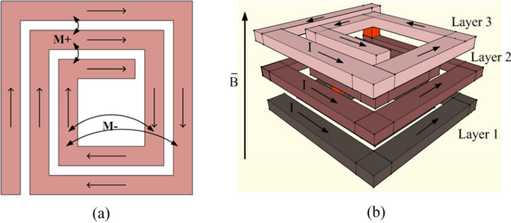
Figure 1. (a) Positive (M+) and negative (M−) mutual inductances in a planar single layer spiral inductor; (b) Concentric flow of current in a three-layer PCB inductor showing the direction of the associated magnetic field.
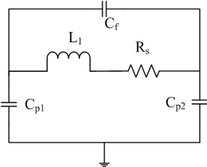
Figure 2. π-model of a single layer inductor.
parallel capacitances from the metal layer to the substrate. For a single layer spiral inductor, Mohan et al. [20] deemed the following equation after Greenhouse [21], which is known as the “Greenhouse formula”,
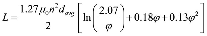 (3)
(3)
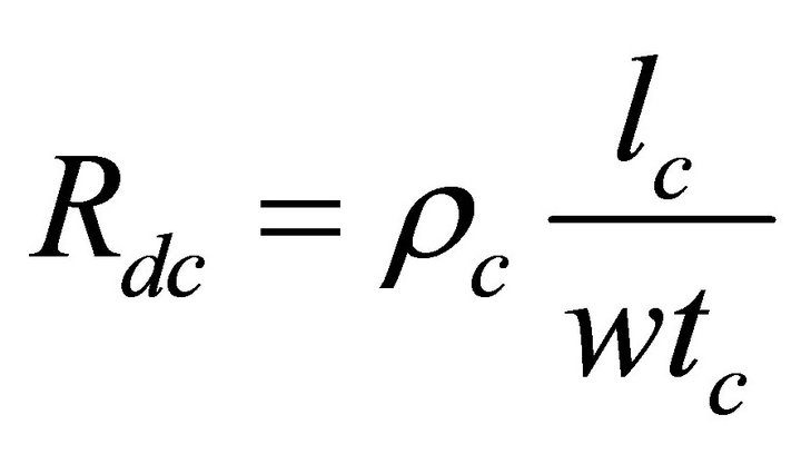
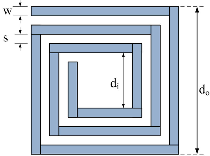
where, n is the number of turns, d0 and di are the outer and inner diameters of the coil, respectively, and φ is the fill factor which is equal to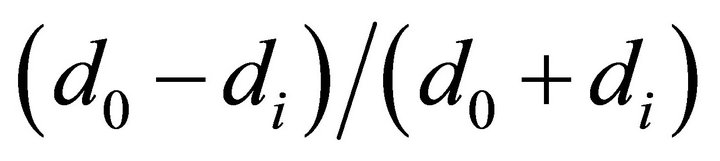 . These geometric parameters are shown in Figure 3. The length of the conductive trace, lc and the DC resistance, Rdc can be expressed as,
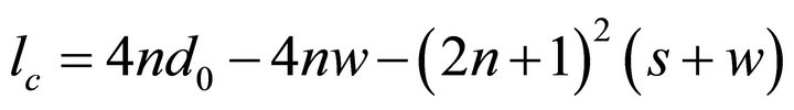 (4)
(4)
 (5)
(5)
where, ρc is the resistivity of the conductive material, tc is thickness, w and s are the line width and the spacing between the metal traces of the inductor, respectively. The skin effect will increase the AC resistance of the coil at higher frequencies and should be taken into account. Considering standard 1 oz. copper (weight of copper in a 1 square foot board), the thickness of the coil in a single layer PCB is 35.56 μm. The skin depth is calculated to be 20.89 μm at 13.56 MHz. Due to the skin effect most of the current will flow through this skin depth resulting in
 (a)
(a)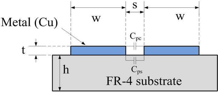 (b)
(b)
Figure 3. Geometrical parameters of a square-shaped PCB inductor. (a) Top view of the PCB inductor; (b) Side view of the PCB inductor.
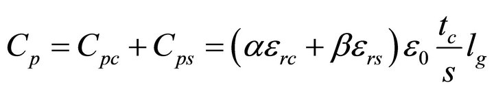
an eventual increase in the resistance. There are two types of insulating materials affecting this capacitance: one is air or the coating insulator that fills the gap between adjacent traces and the other is the PCB substrate, which could be ceramic, polyimide, or FR-4. Total parallel capacitance, Cp of a PCB inductor is given as,
 (6)
(6)
where, Cpc is the capacitance between metal traces through coating, Cps is the capacitance between metal traces through substrate,  dielectric constant of the vacuum, lg is the length of the gap,
  and
and  are the relative dielectric constants of the coating and substrate materials respectively, empirically in the case of air and FR4, α = 0.9 and β = 0.1. The self-resonance frequency (SRF) of the inductor is given by,
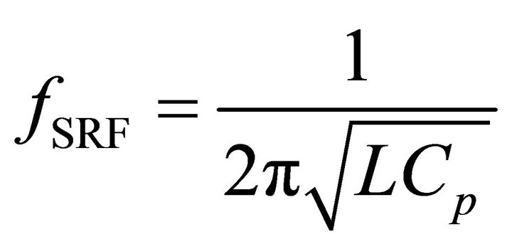 (7)
(7)
2.2.2. Multi-Layer Spiral Inductor
For multi-layer inductors, mutual coupling exists between every layer. Figure 4 illustrates the selfand mutual inductances of three-layer multi-spiral inductor. In this figure, L1, L2, and L3 are the self-inductances of the layers 1, 2, and 3, respectively. M12, M23, and M13 are the mutual inductances between layer 1-2, layer 2-3, and
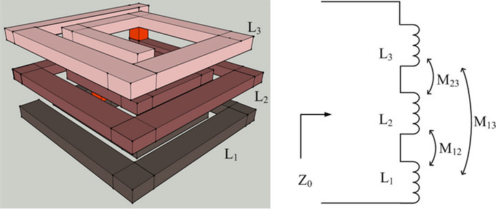
Figure 4. (a) Three layer stacked inductor; (b) Circuit showing the self-inductance and mutual inductance between three metal layers.
layer 1-3 respectively. Considering unidirectional magnetic field and solenoidal structure, the equivalent π-model of single-layer inductor has been expanded for multilayer (i-layer) inductor and the parameters of equivalent π-model are summarized in Table 1.
3. Simulation and Measurement Results
The following design parameters are typically associated with a board level inductor design: 1) the number of the metal layers (l); 2) the spacing between the metal traces (s); 3) the width of the metal trace (w); and 4) the number of turns (n). Simulations have been performed by varying these design parameters using SonnetTM software. Different sets of inductors are fabricated using a commercial 4-layer PCB fabrication process with FR-4 as the substrate material. The fabricated inductor is shown in Figure 5 (marked with red box) and the size of this inductor is compared with a penny.
Fabricated inductors are measured using a 2-port Agilent E8363B PNA network analyzer. The network analyzer is calibrated by the short-open-load-through (SOLT) calibration method by means of standard calibration kits. The measurement setup is shown in Figure 6.
Measurements are taken for frequencies in the range of 10 MHz to 100 MHz. Using the network analyzer, Sparameters (s11, s12, s21, and s22) are measured for each inductor. A MATLAB program is written to convert the S-parameters to Y-parameters. The values of the inductances are calculated from the Y-parameter data. The measurement results with the variation of design parameters are presented in the following sections.
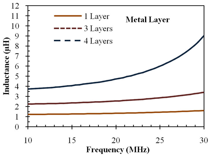
3.1. Variation of Number of Metal Layers (l)
Inductors have been designed with the number of metal layers varying from 1 to 4 and the results are shown in Figures 7(a) and (b). Increasing the number of metal layers increases the inductance value. When the number of metal layer is increased it increases the length of the inductor which in turn increases the value of the inductance (see Table 1). This proves that proper stacking is an effective way to increase the inductance of a structure.
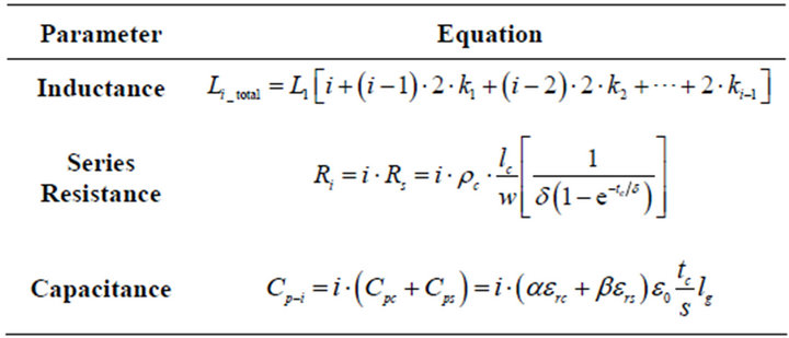
Table 1. Final set of equations for the equivalent Π—model of the i-layer stacked PCB inductor.
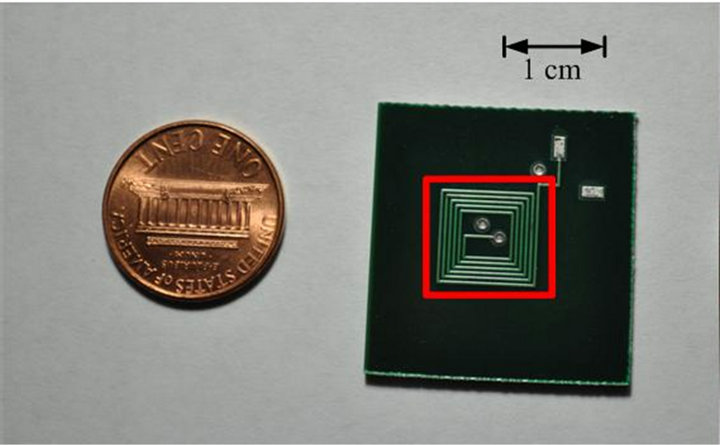
Figure 5. Size of the fabricated inductor (in red box) is compared with the size of a penny.
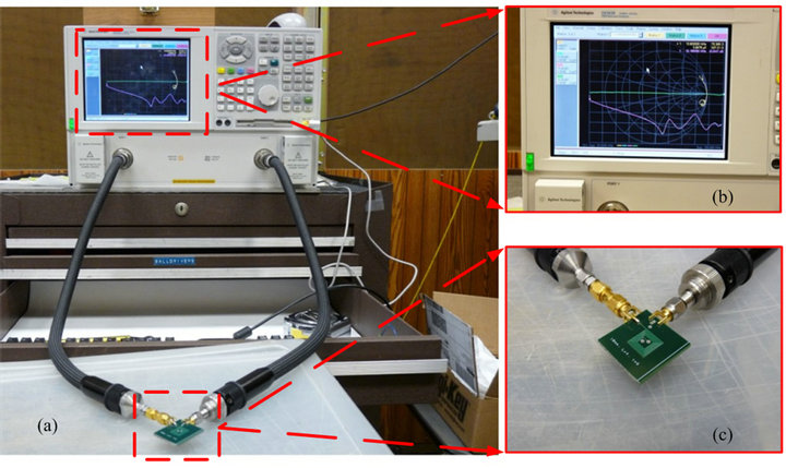
Figure 6. Setup for measuring PCB inductor. (a) PCB inductor with network analyzer; (b) Close view of the network analyzer; (c) Close view of the PCB inductor.
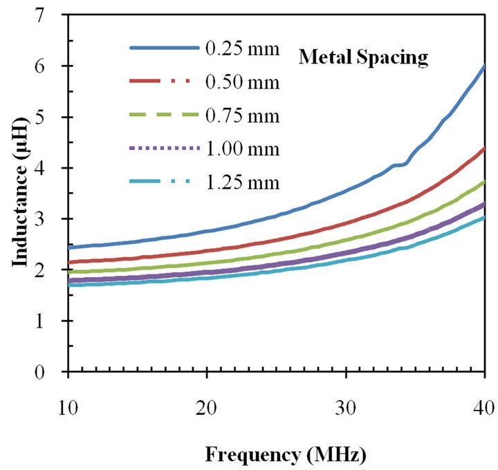
3.2. Variation of Metal Spacing (s)
The spacing (s) between metal traces also changes the effective inductance value. Metal spacing is varied from 0.25 mm to 1.25 mm for the designed inductors and results are shown in Figures 8(a) and (b). For the frequency of 13.56 MHz, the measured values of the inductance are compared with the simulated values in Figure 8(b). It can be seen from the figures that the increase in metal spacing decreases the value of the inductance. When the metal spacing is increased, the mutual coupling between the coils is decreased and as a result the overall inductance is decreased.
 (a)
(a)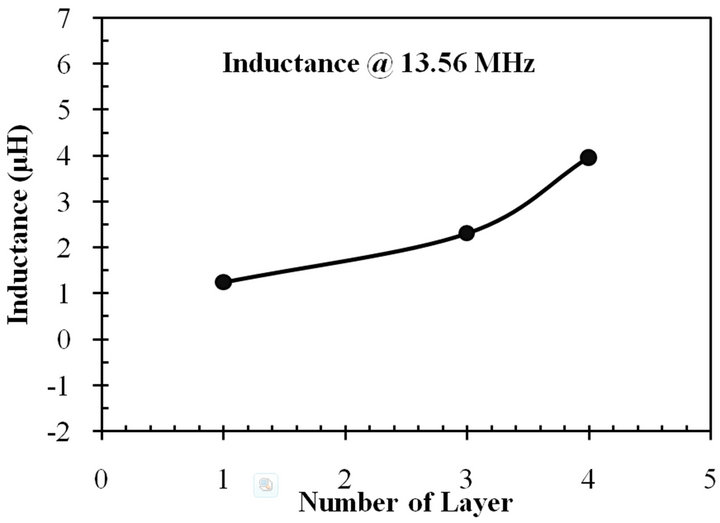 (b)
(b)
Figure 7. (a) Variation of inductance with number of metal layers for PCB inductor; (b) Variation of measured inductance value for varying number of metal layers from 1 to 4 at 13.56 MHz frequency. In this figure, the number of turns is 6, the metal spacing is 0.25 mm, and the metal width is 0.25 mm.
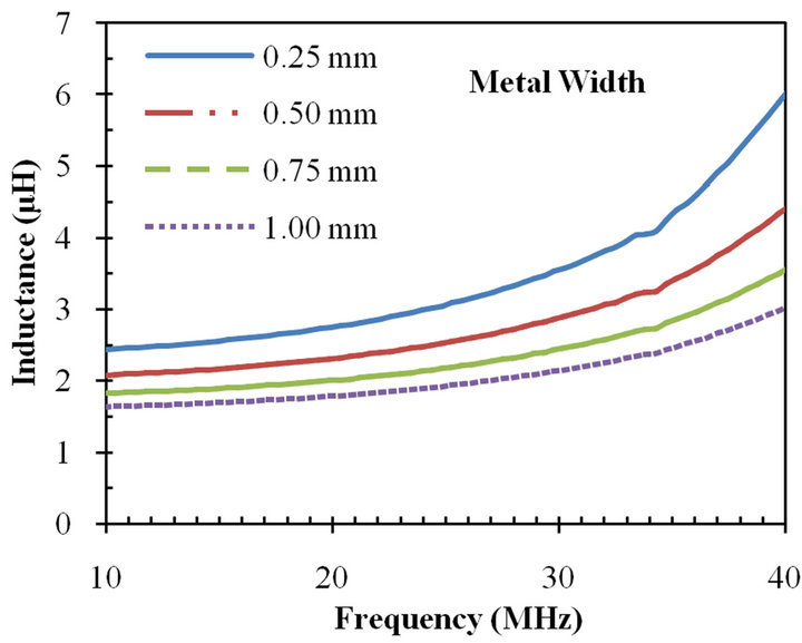
3.3. Variation of Metal Width (w)
Inductance of the designed inductor is also affected by the variation of the metal width (w). The metal width is varied from 0.25 mm to 1 mm for 4-layer PCB inductors. The variation of the inductance with the increase in the metal width is depicted in Figures 9(a) and (b). The inductance is decreased with increase in metal width, which is shown in Figures 9(b) and the measured values are compared with simulated values for 13.56 MHz frequency. It can be seen that as the width is increased the inductance is decreased. The effective length of the total conductor is decreased as a result of the increase in metal width leading to the decrease in the inductance values.
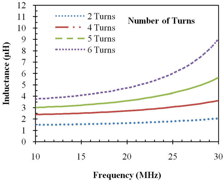
3.4. Variation of Number of Turns (n)
The change of the number of turns (n) affects the inductance of the proposed inductor. The number of turns varied from 2 to 6 for 4-layer PCB inductors. The variation of the inductance with the increase in the number of
 (a)
(a)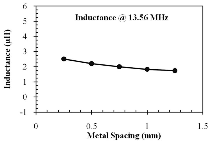 (b)
(b)
Figure 8. (a) Variation of inductance with metal spacing for PCB inductor; (b) Variation of measured inductance value with the increase in metal width for PCB inductor for 13.56 MHz frequency. In this figure, the number of layer is 4, the metal width is 0.25 mm, and number of turns is 6.
turns is illustrated in Figure 10. The inductance is increased as a function of the number of turns following the Greenhouse formula, as shown in Figure 10(b).
4. Design Optimization
The objective of the proposed design is to optimize PCB inductor for biomedical applications. As such, it is desirable to achieve the highest possible inductance and the quality factor for the targeted 13.56 MHz application considering the level of specific absorption rate (SAR) in the human body. Figure-of-merit (FOM) of an inductor is defined by Tai et al. [1] as,
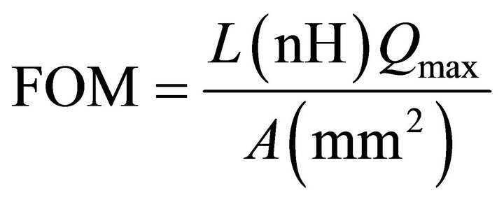 (8)
(8)
Instead of using arbitrary values, the L and Q values at 13.56 MHz are used in Equation (8) to obtain the FOM at
 (a)
(a) (b)
(b)
Figure 9. (a) Variation of inductance with metal width for PCB inductor; (b) Variation of measured inductance value with the increase in metal width for PCB inductor for 13.56 MHz frequency. In this figure, the number of layer is 4, the metal spacing is 0.25 mm, and number of turns is 6.
13.56 MHz (FOM13.56 MHz) for design optimization.
The target of the optimization is to obtain the maximum possible FOM13.56 MHz from the given design constraints. The effects of the variation of the number of layers, metal spacing, metal width and number of turns with respect to FOM13.56 MHz are plotted in Figures 11(a)-(c). It is evident from the figures that lower metal spacing, lower metal width, higher number of metal layers, and higher number of turns can lead to higher FOM13.56 MHz, which is also in accordance with the test results achieved in Section 3. The results are summarized in Figure 11(d). The upper limits of the optimization process are set by the specific PCB process, the number of available metal layers, tooling procedures, the lowest possible metal width, parasitic resistance, the lowest possible spacing between metals, parasitic capacitances, and the SRF. There is a tradeoff between the FOM and the SRF for specific frequency optimization.
The PCB inductor is optimized based on FOM13.56 MHz
 (a)
(a)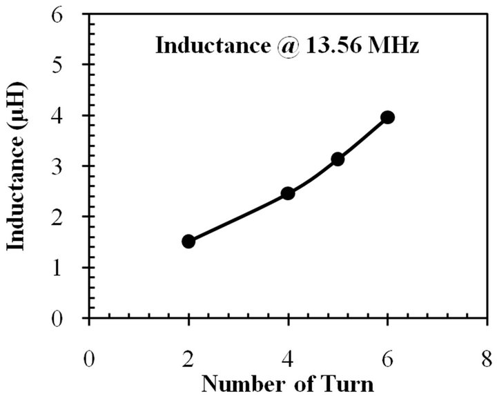 (b)
(b)
Figure 10. (a) Variation of inductance with number of turns for PCB inductor; (b) Variation of measured inductance value with the increase in number of turn for PCB inductor for 13.56 MHz frequency. In this figure, the number of layer is 4, the metal spacing is 0.25 mm, and the metal width is 0.25 mm.
and the design parameters are summarized in Table 2. A good inductance value of 3958.83 nH and the Q value is 23.1 at 13.56 MHz have been achieved with the proposed design scheme which provides a good FOM13.56 MHz of 914.5.
Comparison with State of the Art Work
This work is compared with other PCB inductor designs reported in literature as illustrated in Table 3. The inductance value (L) in each of these cases remains almost constant at low frequencies. The low frequency inductance value and the maximum Q (regardless of the frequency at which the maximum Q occurs) along with the area occupied by the inductors are used following [22] to evaluate the figure-of-merit which reflects the overall performance of the inductor. It needs to be emphasized that different inductors are optimized at different frequencies. Thus for comparison purposes the Q at the op-
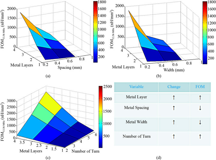
Figure 11. Figure of merit based optimization of PCB inductor with respect to number of layer, metal spacing, width and number of turns. Higher FOM13.56 MHz is obtained for (a) Lower metal spacing and higher metal layer; (b) Lower metal width and higher number of metal layers; (c) Lower metal layer and higher number of turn; (d) Effect of all four design parameters on FOM is summarized. Simulation results are shown here.
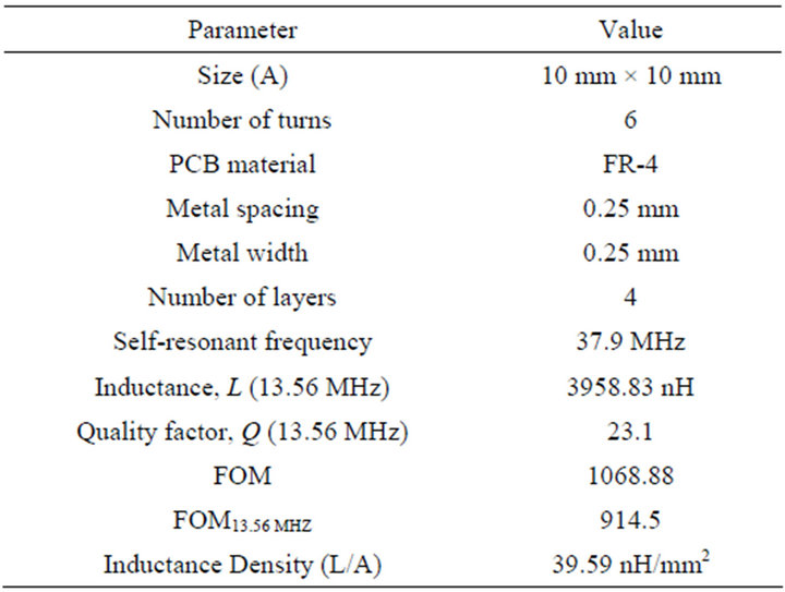
Table 2. Design summary of the proposed PCB inductor.
timized frequency is used to calculate FOM. From the table, it is evident that the proposed scheme demonstrates the highest FOM and the highest inductance density (L/A) compared to other reported works. Ref [12] reported inductors optimized at 13.56 MHz with FOM13.56 MHz calculated to be 306 as compared to 1068 achieved with the
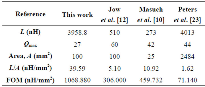
Table 3. Comparison of the designed PCB inductor with works in reported in literature.
proposed multi-spiral inductor. This supports the notion that the multi-spiral solenoidal structure is a successful method of designing high performance inductors.
5. Conclusion
In this paper, design of a multi-spiral solenoidal stacked PCB inductor for biomedical applications has been presented. This stacking method reduces the footprint of the inductor and increases the inductance density. Method of moment based electromagnetic simulation has been performed to design the inductors. A figure-of-merit based optimization technique has been introduced and utilized to optimize the design. A π-model for the multi-spiral inductor is also proposed based on the empirical formulas. PCB inductors occupying an area of 100 mm2 are fabricated using a commercial 4-layer fabrication process. Measurements have been carried out and the test results are presented. Test results demonstrate that the proposed inductor provides higher inductance, good inductance density, and a better figure of merit value compared to similar works reported in literature. This leads to higher link efficiency of the overall system.
6. Acknowledgements
The authors would like to thank Dr. Aly Fathy and Mr. Yun Seo Koo for their outstanding support regarding simulation and measurement respectively.
REFERENCES
- S. A. Jaffari and A. P. F. Turner, “Recent Advances in Amperometric Glucose Biosensors for in Vivo Monitoring,” Physiological Measurement, Vol. 16, No. 1, 1995, pp. 1-15. doi:10.1088/0967-3334/16/1/001
- E. Renard, “Implantable Glucose Sensors for Diabetes Monitoring,” Minimally Invasive Therapy & Allied Technologies, Vol. 13, No. 2, 2004, pp. 78-86. doi:10.1080/13645700410026993
- M. Zhang, M. R. Haider, M. A. Huque, M. A. Adeeb, S. R. Rahman and S. K. Islam, “A Low Power Sensor Signal Processing Circuit for Implantable Biosensor Applications,” Smart Materials & Structures, Vol. 16, No. 2, 2007, pp. 525-530. doi:10.1088/0964-1726/16/2/034
- D. A. Baker and D. A. Gough, “A Continuous, Implantable Lactate Sensor,” Analytical Chemistry, Vol. 67, No. 9, 1995, pp. 1536-1540. doi:10.1021/ac00105a010
- C. Hierold, B. Clasbrummel, D. Behrend, T. Scheiter, M. Steger, K. Oppermann, H. Kapels, E. Landgraf, D. Wenzel and D. Etzrodt, “Low Power Integrated Pressure Sensor System for Medical Applications,” Sensors and Actuators A-Physical, Vol. 73, No. 1-2, 1999, pp. 58-67. doi:10.1016/S0924-4247(98)00255-6
- R. Bashirullah, “Wireless Implants,” IEEE Microwave Magazine, Vol. 11, No. 7, 2010, pp. S14-S23. doi:10.1109/MMM.2010.938579
- C. Sauer, M. Stanacevic, G. Cauwenberghs and N. Thakor, “Power Harvesting and Telemetry in CMOS for Implanted Devices,” IEEE Transactions on Circuits and Systems I: Regular Papers, Vol. 52, No. 12, 2005, pp. 2605-2613.
- M. M. Ahmadi and G. A. Jullien, “A Wireless-Implantable Microsystem for Continuous Blood Glucose Monitoring,” IEEE Transactions on Biomedical Circuits and Systems, Vol. 3, No. 3, 2009, pp. 169-180. doi:10.1109/TBCAS.2009.2016844
- A. M. Sodagar, K. D. Wise and K. Najafi, “A Wireless Implantable Microsystem for Multichannel Neural Recording,” IEEE Transactions on Microwave Theory and Techniques, Vol. 57, No. 10, 2009, pp. 2565-2573. doi:10.1109/TMTT.2009.2029957
- J. Masuch and M. Delgado-Restituto, “Design Constraints for the Inductive Power and Data Link of an Implanted Body Sensor,” Proceedings of the European Conference on Circuit Theory and Design, Antalya, 23-27 August 2009, pp. 425-428.
- M. AhsanulAdeeb, “A Class E Inductive Powering Link with Backward Data Communication for Implantable Sensor Systems,” Ph.D. Thesis, The University of Tennessee, Knoxville, 2006.
- J. Uei-Ming and M. Ghovanloo, “Design and Optimization of Printed Spiral Coils for Efficient Inductive Power Transmission,” Proceedings of the 14th IEEE International Conference on Electronics, Circuits and Systems, Marrakech, 11-14 December 2007, pp. 70-73.
- M. R. Shah, R. P. Phillips and R. A. Normann, “A Study of Printed Spiral Coils for Neuroprosthetic Transcranial Telemetry Applications,” IEEE Transactions on Biomedical Engineering, Vol. 45, No. 7, 1998, pp. 867-876. doi:10.1109/10.686794
- J. A. Von Arx and K. Najafi, “A Wireless Single-Chip Telemetry-Powered Neural Stimulation System,” IEEE Proceedings of the International Solid-State Circuits Conference, 1999, pp. 214-215.
- S. Kim, M. Wilke, M. Klein, M. Toepper and F. Solzbacher, “Electromagnetic Compatibility of Two Novel Packaging Concepts of an Inductively Powered Neural Interface,” Proceedings of the 3rd International IEEE/ EMBS Conference on Neural Engineering, Kohala Coast, 2-5 May 2007, pp. 434-437.
- F. C. Commission, “Guidelines for Evaluating the Environmental Effects of Radio Frequency Radiation,” 1996.
- Sonnet, “Sonnet Software,” 12.56 Edition, 2010.
- F. W. Grover, “Inductance Calculations,” Van Nostrand, Princeton, 1946.
- E. B. Rosa, “The Self and Mutual Inductances of Linear Conductors,” Bulletin of the Bureau of Standards, Vol. 4, No. 2, 1908, pp. 301-344. doi:10.6028/bulletin.088
- S. S. Mohan, M. M. Hershenson, S. P. Boyd and T. H. Lee, “Simple Accurate Expressions for Planar Spiral Inductances,” IEEE Journal of Solid-State Circuits, Vol. 34, No. 10, 1999, pp. 1419-1424. doi:10.1109/4.792620
- H. Greenhouse, “Design of Planar Rectangular Microelectronic Inductors,” IEEE Transactions on Parts, Hybrids, and Packaging, Vol. 10, No. 2, 1974, pp. 101-109. doi:10.1109/TPHP.1974.1134841
- C.-M. Tai and C.-N. Liao, “Multilevel Suspended Thin Film Inductors on Silicon Wafers,” IEEE Transactions on Electron Devices, Vol. 54, No. 6, 2007, pp. 1510-1514. doi:10.1109/TED.2007.896347
- C. Peters and Y. Manoli, “Inductance Calculation of Planar Multi-Layer and Multi-Wire Coils: An Analytical Approach,” Sensors and Actuators A-Physical, Vol. 145-146, 2008, pp. 394-404. doi:10.1016/j.sna.2007.11.003