Circuits and Systems
Vol. 3 No. 1 (2012) , Article ID: 16658 , 8 pages DOI:10.4236/cs.2012.31013
Design and Analysis of a Power Efficient Linearly Tunable Cross-Coupled Transconductor Having Separate Bias Control
1Electronics and Communication Engineering Department, Motilal Nehru National Institute of Technology, Allahabad, India
2Department of Computer Engineering and Application, GLA University, Mathura, India
3Electronics and Electrical Communication Engineering Department, Indian Institute of Technology, Kharagpur, India
Email: *vijaya@mnnit.ac.in, Krishna.kant@gla.ac.in, swapna@ece.iitkgp.ernet.in
Received November 12, 2011; revised December 15, 2011; accepted December 24, 2011
Keywords: Analog Electronics; Low Power Analog CMOS Circuit; Operational Transconductance Amplifier (OTA); Multiple-Output OTA (MOTA); MOS Transconductors; Linearly Tunable Gm; Current Efficiency; Linearization Techniques; Harmonic Distortion Analysis
ABSTRACT
A common current source, generally used to bias cross-coupled differential amplifiers in a transconductor, controls third harmonic distortion (HD3) poorly. Separate current sources are shown to provide better control on HD3. In this paper, a detailed design and analysis is presented for a transconductor made using this biasing technique. The transconductor, in addition, is made to offer high Gm, low power dissipation and is designed for linearly tunable Gm with current mode load as one of the applications. The circuit exhibits HD3 of less than –43.7 dB, high current efficiency of 1.18 V−1 and Gm of 390 mS at 1 Vp-p @ 50 MHz. UMC 0.18 µm CMOS process technology is used for simulation at supply voltage of 1.8 V.
1. Introduction
Transconductors interface a current mode circuit to a voltage signal, making it a fundamental element of analog circuits [1-4]. Performance of a transconductor deteriorates due to higher total harmonic distortion (THD), more so at high signal level. Several techniques are devoted to improve THD of transconductors [5-20]. Sánchez-Sinencio and J. Silva-Martínez [4] have classified these as input signal attenuation [5-7], cancellation of nonlinear terms [7-12], and source degeneration [7, 11-19]. Besides these, adaptive biasing [16,19] and mobility compensation [20] techniques are also reported to improve THD.
One of the important building blocks in many analog circuits is a tunable linear transconductor [9,13,15,17, 21-25], which may be used for tuning center frequency and Q-factor of filters. Moreover it helps to compensate fabrication tolerances and environment parameters, especially temperature.
A method of tuning transconductance, Gm is to control the bias current (IBias) applied to the differential amplifier. But Gm is proportional to the square root of IBias due to which the allowable input signal swing is limited to small value [1]. In [17], the allowable input swing for a constant value of IBias is made independent of variation in Gm by using current mirrors with source degeneration.
Another tuning method uses source degeneration resistance (R). In this method due to degeneration, THD improves but at the cost of transconductance. Further, the condition of improvement, (1/Gm < R) [1] occupies large area and add noise if passive resistance is used. In [13], tunability has been achieved using active resistance. But Gm adjustment in this tuning method affects the bandwidth, which has been compensated in [15] by employing a separate source follower biased with constant current source.
Linearly adjustable Gm is realized using control voltage at inputs of one of the cross-coupled differential amplifier [8,9]. In both the papers authors have used identical transistors in the cross-coupled amplifiers to obtain linear tuning of Gm at supply voltage 5 V or higher. Different bias strategies are given in [25] to achieve tunability for ultra low range transconductance.
A low voltage transconductor on 0.18 µm technology is given by us in [23] in which bias currents of crosscoupled differential amplifiers and aspect ratio of their transistors are adjusted to cancel third harmonic distortion. Shift level biasing is used in the cross-coupled differential amplifier to obtain tunability. The circuit is designed for resistive load, not suitable for current mode signal processing.
The topology cited in [23] is analyzed in detail in this paper. In addition diode mode MOSFETs are used as load for current mode signal processing in place of active resistance. A triode mode tail transistor is used in MA for better linear tuning instead of constant current source. Design steps in detail with algorithm are given for low HD3, high linearly tunable Gm and high frequency of operation at low voltage. Efforts have also been made to maintain low power operation and high current efficiency. The circuit is developed for 1 Vp–p input signal for frequency range upto 50 MHz.
The paper is organized as follows. In Section 2, block diagram, circuit design alongwith its algorithm and analysis of the proposed circuit are given. In Section 3, simulation results are discussed and finally conclusions are drawn in Section 4.
2. Design and Analysis of Tunable Transconductor
2.1. Block Diagram of Tunable Transconductor
The proposed transconductor is designed using main differential amplifier (MA) biased using tail transistors in triode mode, compensatory differential amplifier (CA) biased using separate constant current source for minimizing HD3 and level shifters (LS) are used for tunability. Separate controls of the two bias currents of MA and CA provide flexibility, improvement in HD3 and better tuning in comparison to others [8,9]. Block diagram of the proposed transconductor is shown in Figure 1 and the complete circuit diagram is furnished in Figure 2.
The square law model of MOSFETs is used in this work for design and analysis. Design steps are given below:
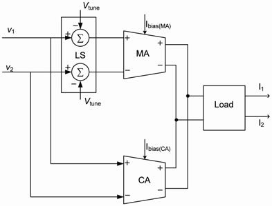
Figure 1. Functional block diagram of the trnsconductor.
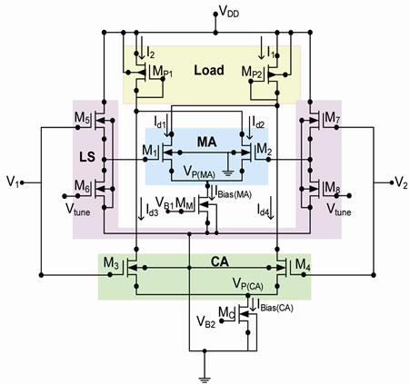
Figure 2. Circuit diagram of the transconductor.
2.1.1. Design of MA
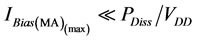
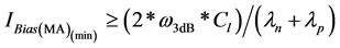
Upper limit and lower limit of biasing current ( ) for MA are given as follows [3]:
 (1)
(1)
 (2)
(2)
where PDiss is the specified total power consumption, Cl is the load capacitor, ω3dB is the 3 dB frequency, λn and λp are the channel length coefficients of NMOS and PMOS transistors respectively. MA is designed using NMOS transistors and load using PMOS transistors.
Transconductance,  of MA and input swing,
  are given in [1,3] and are reproduced in Equation (3) and Equation (4).
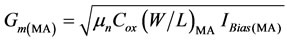 (3)
(3)
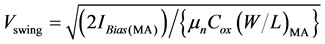 (4)
(4)
From Equation (3)  is the function of
  and
and . To keep high
 , higher values of
  are not used as it would lead to loss of power. The second option is to increase the aspect ratio but that may deteriorate HD3 for specified input swing {Equation (4)}.
The second option is preferred wherein, for better HD3, the method of non-linear terms cancellation with the help of compensatory amplifier is used but at the cost of area occupied by it. However, the use of CA (Figure 2) reduces overall transconductance. To maintain transconductance  of the OTA at the desired level,
  is adjusted {Equation (7)}. For high current efficiency (
 ),
), is selected slightly greater than
  and aspect ratio
  is determined from Equation (3) for the modified value of
 . In addition,
  is allowed to vary independently of CA as a function of tuning voltage by operating tail transistor of MA in triode mode.
2.1.2. Design of CA
The ratio “p” of bias currents of MA and CA are adjusted [11,12] in accordance with Equation (5):
 (5)
(5)
where  and
and
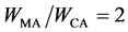
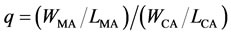 . A lower value of “q” not only increases power dissipation (due to high bias current of CA), but also lowers the overall transconductance, thereby, decreasing the current efficiency. On the other hand, due to higher values of “q” the harmonics will not be suppressed effectively. Moreover, it is difficult to bias the CA transistor in saturation region in the specified low voltage operation due to skewed overdrive voltages of the MA and CA. In the proposed circuit choosing a moderate “q” as 2 and equal channel length of MA and CA gives:
 (6)
(6)
and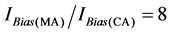 . This ratio of bias currents is adjusted for the centre value of the tuning voltage range at which specified Gm is expected to occur.
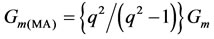
Overall transconductance  due to cross-coupling of MA and CA is the difference of
  and
and , hence
  is selected to get the specified Gm in accordance of Equation (7).
 (7)
(7)
2.1.3. Design of Load
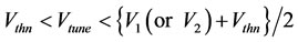
The PMOS transistors, Mp1 and Mp2 are selected in diode mode as load. It is possible to easily convert the proposed transconductor to Multiple-output OTA suitable for current mode signal processing by incorporating three current mirrors. The aspect ratio of load transistors is computed using the Equation (8), where in Equation (8)  is the maximum common mode input voltage at MA, Vthn and Vthp are the threshold voltages of NMOS and PMOS transistors respectively.
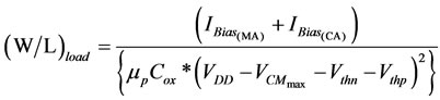 (8)
(8)
2.1.4. Design of LS
Linearly tunable Gm is obtained by modulating common mode voltage with Vtune in two level shifters. The transistors (M5 and M6) of a level shifter of LS are selected to have same aspect ratio to maintain same Vtune across gate to source in both the transistors. They are biased in saturation region by following the conditions given in Equation (9) and Equation (10).
 (9)
(9)
 (10)
(10)
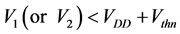
where  and
and  are the signal inputs applied at the gates of M5 and M7 of level shifters, respectively. Same input V1 and V2 are applied to the gate of M3 and M4 of CA. As per the Equation (10) higher values of V1 (or V2) give better tuning range, accordingly, VDC is selected slightly less than to VDD. Further, MA remains in saturation if and only if condition given in Equation (11) is satisfied.
 (11)
(11)
where  is the drain to source voltage of tail transistor of MA Thus, the limits on Vtune are obtained as in Equation (12). Transistors of other level shifter of LS are also made identical on the same ground.
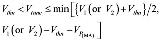 (12)
(12)
2.1.5. Design of Tail Transistor of MA
As the bias current supplied to MA by its tail transistor is a function of tuning voltage, it is operated in triode mode. It needs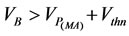 , where
  is gate voltage of tail transistor of MA. The aspect ratio of tail transistor of MA is derived for the mentioned operating mode and is given in Equation (13):
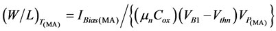 (13)
(13)
2.1.6. Design of Tail Transistor of CA
Tail transistor of CA is chosen as constant current source independent of  by biasing the transistor in saturation. The aspect ratio of it is given in Equation (14):
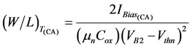 (14)
(14)
where  is gate voltage of tail transistor of CA.
2.2. Algorithm for Designing the Proposed Transconductor
The algorithm to design proposed transconductor is summarized as below:

2.3. Analysis of the Circuit
The analysis of the circuit is given below:
In Figure 2, applying the square law to the transistors of MA and CA, which are biased in saturation region, the currents, I1 and I2 through load transistors of the cross-coupled amplifiers (MA-CA) are given by:
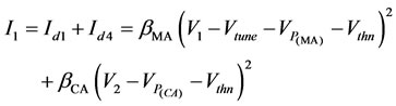 (15)
(15)
 (16)
(16)
where  is the transconductance parameter.
  and
and  are the drain to source voltage across tail transistor of MA and CA respectively.
The differential output current, io is given by
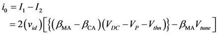 (17)
(17)
where 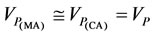 is assumed.
Since “q” is taken as 2 to minimize HD3:
 (18)
(18)
Combining Equation (17) and Equation (18), one gets:
 (19)
(19)
From Equation (19) the transconductance Gm is calculated as,
 (20)
(20)
Equation (20) shows linear behaviour of Gm with Vtune, as first part,  on the right hand side of the equation is almost constant. Thus from Equation (20) the tuning range is obtained and is given in Equation (21).
 (21)
(21)
3. Simulation Results and Discussions
The proposed transconductor is simulated in Cadence VIRTUOSO environment using UMC 0.18 µm CMOS process technology. The transconductor is operated at 1.8 V and 27˚ Celsius. Bias currents  and
and  are kept at 200 µA and 25 µA, respectively to maintain
 . Channel length is taken as 0.9 µm which is five times the minimum as specified by the technology for all the MOSFETs of the transconductor to minimize channel length modulation effect [26]. The differential signal input voltage of 0.25 V is generated using voltage controlled voltage source (VCVS) as test bench setup.
The objective of the simulation is to demonstrate feasibility of power efficiency, linear tuning of Gm offering low harmonics with the help of separate bias control of cross-coupled amplifiers at 50 MHz and above. Different plots have been obtained to verify the designed aspects.
Plot in Figure 3 shows the tunability of the proposed transconductor. The tuning voltage, Vtune is varied from 0.5 V to 1.0 V in steps of 0.1 V. The lower value (0.5 V) is kept slightly higher than the threshold voltage of input transistors M5 and M7 of LS and upper value is selected as per Equation (12) to keep them in saturation region. Gm is tuned between 390 µS to 195 µS. Gm is falling with increase in  between ±0.25 V of vid i.e. 1 Vp-p, However for higher values of vid, (around ±0.5 V i.e. 2 Vp–p) the change in Gm w.r.t. Vtune is nonlinear and plots for different values of Vtune are almost merged at a point, indicates transconductance is independent of Vtune. The reason being that as per Equation (12),
  , but at higher values, this condition is violated. At
 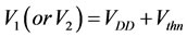 transistor M5 and M7 of Figure 2 are at the verge of saturation, and variation in drain to source voltage across it is small enough, making output of level shifter is almost constant, i.e. independent of tuning voltage.
As shown in Figure 4 the variation of transconductance with respect to tuning voltage is linear validating Equation (20). The small deviation may be attributed to body effect in LS transistors (M5 and M7) and voltage drop in tail transistors.
Figure 5 shows HD3 variation with respect to differential input signal amplitude for different values of tuning voltage. Distortion increases rapidly for the small values i.e. upto approximately 150 mV (0.6 Vp–p) of the differential input signal amplitude but after that it in creases
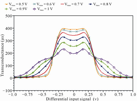
Figure 3. Transconductance (Gm) vs differential signal input (vid) at different values of tuning voltage (Vtune).
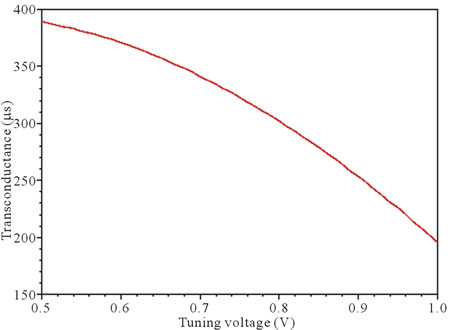
Figure 4. Transconductance (Gm) vs tuning voltage (Vtune) at differential signal input (vid) = 0 V.
slowly due to cross-coupling effect. Harmonic distortion has also increased with the increase in tuning voltage due to decrease in DC current through MA. Figure 6 shows variation of HD3 with respect to Vtune.
Frequency response of the proposed transconductor for different values of tuning voltage is given in Figure 7. The 3 dB frequency of the transconductor is above 53 MHz for the complete range of variation of transconductance.
Gm, HD3, PDiss and Gm/IDD for the three different values of Gm obtained from the simulation are given in Table 1. It may be noted that at lower values of transconductance current efficiency reduces. The reasons are twofold: firstly, transconductance is low and secondly lower transconductance obtained at higher value of tuning voltage, gives high overdrive voltage to LS transistors which in turn draws higher current through LS.
The performance is compared on eight metric points with other reported circuits as given in Table 2. The proposed transconductor offers better current efficiency
Figure 5. HD3 vs differential signal input (vid) at different tuning voltage (Vtune).
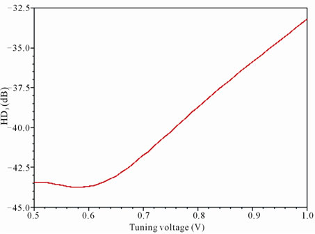
Figure 6. HD3 vs Tuning voltage at differential signal input (vid) = 0.25 V.
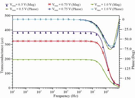
Figure 7. Transconductance vs frequency at different tuning voltage (Vtune).
(1.18 V–1) and transconductance (390 µS) with lower harmonics (–43.7 dB), at input swing of 1 Vp–p @50 MHz in comparison to the others. However, the transconductance reported in [9] is higher than the proposed at the cost of high supply voltage (5 V) and very low current efficiency (0.1 V–1 to 0.07 V–1).
4. Conclusions
A power efficient linearly tunable high Gm, cross-coupled transconductor with separate bias currents (for low third harmonic distortion) is designed and analyzed in this paper. Results have been obtained with diode mode transistors as load extendable for MOTA, which is necessary for current mode signal processing. Transconductance is varied in linear manner. Gm is tuned between 195 to 390 mS when the tuning voltage is varied from 1.0 V to 0.5 V. Maximum current efficiency of 1.18 V–1 and minimum HD3 less than –43.7 dB is obtained at 1 Vp–p @ 50 MHz at the tuning voltage of 0.5 V. Comparative study reveals that the proposed circuit consumes low power and gives high current efficiency, with low HD3 and high tunable transconductance for high frequency of operation compared to others.
5. Acknowledgements
This work has been performed using the resources of VLSI Laboratory developed under Special Manpower Development Programme for VLSI Design and related software (SMDP-II) project funded by Department of
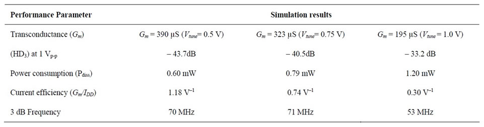
Table 1. Performance of proposed transconductor.
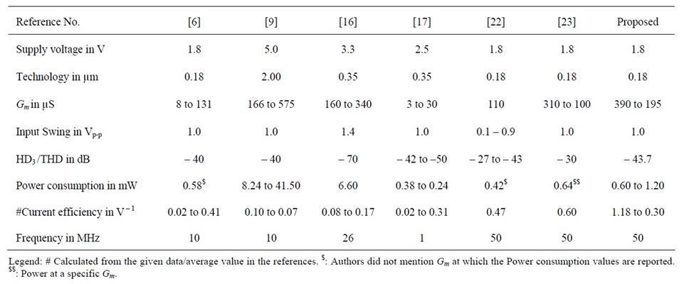
Table 2. Performance comparison of proposed transconductors with others.
Information Technology, Ministry of Communication and Information Technology Government of India.
REFERENCES
- B. Razavi, “Design of Analog CMOS Integrated Circuits,” Tata McGraw-Hill Publishing Company Limited, 2002.
- D. A. Johns and K. Martin, “Analog Integrated Circuit Design,” John Wiley and Sons, New York, 1997.
- P. E. Allen and D. R. Holberg, “CMOS Analog Circuit Design,” Oxford University Press, New York, 2004.
- E. Sánchez-Sinencio and J. Silva-Martínez, “CMOS Transconductance Amplifiers, Architectures and Active Filters: A Tutorial,” IEE Proceedings Circuits, Devices & Systems, Vol. 147, No. 1, 2000, pp. 3-12. doi:10.1049/ip-cds:20000055
- J. Y. Kim and R. L. Geiger, “Characterisation of Linear MOS Active Attenuator and Amplifier,” Electronic Letters, Vol. 31, 1995, pp. 511-513. doi:10.1049/el:19950353
- X. Zhang and E. I. El-Masry, “A Novel CMOS OTA Based on Body-Driven MOSFETs and Its Applications in OTA-C Filters,” IEEE Transactions on Circuits and System-I Regular Papers, Vol. 54, No. 6, 2007, pp. 1204- 1211. doi:10.1109/TCSI.2007.897765
- J. Chen, E. Sanchez-Sinencio and J. Silva-Martinez, “Frequency Dependent Harmonic Distortion Analysis of a Linearized cross Coupled CMOS OTA and Its Application to OTA C-Filter,” IEEE Transactions on Circuits and System-I Regular Papers, Vol. 53, No. 3, 2006, pp. 499-510. doi:10.1109/TCSI.2005.859575
- Z. Wang and W. Guggenbuhl, “A Voltage-Controlled Linear MOS Transconductor Using Bias Offset Technique,” IEEE Journal of Solid-State Circuits, Vol. 25, 1990, pp. 315-317. doi:10.1109/4.50321
- Y. Sun, C. Hill and S. Szczepanski, “Large Dynamic Range High Frequency Fully Differential CMOS Transconductance Amplifier,” Analog Integrated Circuits and Signal Processing, Vol. 34, 2003, pp. 247-255.
- D. V. Morozov and A. S. Kuroki, “Transconductance Amplifier with Low-Power Consumption,” IEEE Transactions on Circuits and System-II Express Briefs, Vol. 52, No. 11, 2005, pp. 776-779. doi:10.1109/TCSII.2005.852190
- A. Lewinski and J. Silva-Martinez, “OTA Linearity Enhancement Technique for High Frequency Application With IM3 Below-65 dB,” IEEE Transactions on Circuits and System-II Express Briefs, Vol. 51, No 10, 2004, pp. 542-548. doi:10.1109/TCSII.2004.834531
- S. Ouzounov, E. Roza, H. Hegt, G. V. D. Weide and A. V. Roermund, “Design of MOS Transconductors with Low Noise and Low Harmonic Distortion for Minimum Current Consumption,” Integration, the VLSI Journal, Vol. 40, 2007, pp. 365-379.
- F. Krummenacher and N. Joehl, “A 4-MHz CMOS Continuous-Time Filter with On-Chip Automatic Tuning,” IEEE Journal of Solid-State Circuits, Vol. 23, No. 3, 1988, pp. 750-758. doi:10.1109/4.315
- J. Silva-Martinez, M. S. J. Steyaert and W. M. C. Sansen, “A Large-Signal Very Low-Distortion Transconductor for High-Frequency Continuous-Time Filters,” IEEE Journal of Solid-State Circuits, Vol. 26, No. 7, 1991, pp. 946-954. doi:10.1109/4.92014
- M. Kachare, A. J. Lopez-Martin, J. Ramirez-Angulo, and R. G. Carvajal, “A Compact Tunable CMOS Transconductor with Linearity,” IEEE Transactions on Circuits and System-II Express Briefs, Vol. 52, No. 2, 2005, pp. 82-84. doi:10.1109/TCSII.2004.842065
- W. Huang and E. Sanchez-Sinencio, “Robust HighlyLinear High-Frequency CMOS OTA with IM3 Below-70 dB at 26 MHz,” IEEE Transactions on Circuits and System-I Regular Papers, Vol. 53, No. 7, 2006, pp. 1433- 1447. doi:10.1109/TCSI.2006.875187
- F. A. P. Baruqui and A. Petraglia, “Linearly Tunable CMOS OTA With Constant Dynamic Range Using Source-Degenerated Current Mirrors,” IEEE Transactions on Circuits and System-II Express Briefs, Vol. 53, No. 9, 2006, pp. 797-801. doi:10.1109/TCSII.2006.881162
- P. Monsurrò, S. Pennisi, G. Scotti and A. Trifiletti, “Linearization Technique for Source-Degenerated CMOS Differential Transconductors,” IEEE Transactions on Circuits and System-II, Vol. 54, No. 10, 2007, pp. 848- 852. doi:10.1109/TCSII.2007.906203
- K. Kuo and A. Leuciuc, “A Linear MOS Transconductor Using Source Degeneration and Adaptive Biasing,” IEEE Transactions on Circuits and System-II Express Briefs, Vol. 48, No. 10, 2001, pp. 937-943. doi:10.1109/82.974782
- S. H. Yang, K. H. Kim, Y. You and K. R. Cho, “A Novel CMOS Operational Transconductance Amplifier Based on Mobility Compensation Technique,” IEEE Transactions on Circuits and System-II Express Briefs, Vol. 52, No. 1, 2005, pp. 37- 42. doi:10.1109/TCSII.2004.839539
- S. Koziel and S. Szczepanski, “Design of Highly Linear Tunable CMOS OTA for Continuous-Time Filters,” IEEE Transactions on Circuits and System-II Analog and Digital Signal Processing, Vol. 49, No. 2, 2002, pp. 110-122. doi:10.1109/TCSII.2002.1002513
- A. A. Fayed and M. Ismail, “A Low Voltage, Highly Linear Voltage-Controlled Transconductor,” IEEE Transactions on Circuits and System-II Express Briefs, Vol. 52 No. 12, 2005, pp. 831-835. doi:10.1109/TCSII.2005.853511
- V. Bhadauria and K. Kant, “A Novel Technique for Tuning Low Voltage Linear Transconductor,” 2010 International Conference on Electronic Devices, System and Application (ICEDSA2010), 12-13 April 2010, Kuala Lumpur, Malaysia, pp. 22-25. doi:10.1109/ICEDSA.2010.5503108
- V. Bhadauria K. Kant and S. Banerjee, “A Tunable Transconductor with High Linearity,” Proceedings of Asia Pacific Conference on Circuits and Systems (APCCAS 2010), Kuala Lumpur, 6-9 December 2010, pp. 5-8. doi:10.1109/APCCAS.2010.5774749
- P. Bruschi, F. Sebastiano and N. Nizza, “CMOS Transconductors with Nearly Constant Input Ranges over wide Tuning Intervals,” IEEE Transactions on Circuits and System-II Express Briefs, Vol. 53, No. 10, 2006, pp. 1002- 1006. doi:10.1109/TCSII.2006.882126
- R. J. Baker, “CMOS Circuit Design, Layout, and Simulation,” IEEE Press, Wiley-Interscience, A John Wiley & sons, Inc., Publication, New York, 2005, Chapter 9, p. 291.
NOTES
*Corresponding author.