Int'l J. of Communications, Network and System Sciences
Vol.3 No.2(2010), Article ID:1274,6 pages DOI:10.4236/ijcns.2010.32027
CPW Fed Double T-Shaped Array Antenna with Suppressed Mutual Coupling
1Department of Electrical Engineering, Islamic Azad University (IAU),Science and Research Branch, Tehran, Iran
2Department of Electrical Engineering, Islamic Azad University,Shahr_e_Rey Branch, Tehran, Iran
E-mail: alexdanideh@gmail.com, alotfi@iust.ac.ir
Received November 19, 2009; revised December 22, 2009; accepted December 29, 2009
Keywords: CPW, T-Shaped Antenna, WLAN, MIMO, Mutual Coupling
Abstract
A compact CPW-fed double T-Shaped antenna is proposed for dual-band wireless local area network (WLAN) operations. For the proposed antenna, the -10 dB return loss bandwidth could reach about 25.5% for the 2.4 GHz band and 5.7 % for the 5 GHz band, which meet the required bandwidth specification of WLAN standard. To reduce the mutual coupling and get high isolation between two dual-band antennas, we proposed the novel electromagnetic band gap (EBG) structures. When the EBG structure is employed, a -13dB and -30dB mutual coupling reduction is achieved at 2.4 and 5.2 GHz. It shows that the features of small size, uniplanar structure, good radiation characteristics and small mutual coupling are promising for multi-input multi-output (MIMO) applications.
1. Introduction
Wireless communications, especially the wireless local area network (WLAN) communication, have evolved at astonishing rate during the last decade. Therefore, design of broad dual and multi-band antennas with low-profile, lightweight, flush mounted and single-feed to fit the limited equipment space of the WLAN device has gained increasing demands. Coplanar waveguide (CPW) transmission lines have been widely used as feeding networks with slot antennas. CPW lines have many useful design characteristics such as low radiation leakage, less dispersion, little dependence of the characteristic impedance on substrate height, and uniplanar configuration. They also allow easy mounting and integration with other microwave integrated circuits and RF frequency devices. Dualband operations have become very important in wireless local area network (WLAN) applications. CPW-fed antennas for wireless communications have been discussed by many authors for dual-band operations.
The demand for high speed and high quality data transmission in communications has been rapidly increasing .This requires the effective utilization of the limited channel bandwidth. At the same time, multi-input multi-output (MIMO) systems have also received significant attention for their ability to increase the channel capacity.
A novel and simple printed dual-band with two different sizes T-shaped antenna which generates two separate resonant is proposed in [1].
Since WLAN antennas are usually required on broad bandwidth and small antenna size, researchers have studied monopole structures with dual resonant modes [2–4].
A new CPW-fed T-shaped monopole antenna with a trapeze form ground plane and two parasitic elements for WLAN/WiMAX dual mode operation is investigated in [5].
The CPW-fed G-shaped planar monopole antenna with dual band operation is a good choice for WLAN application [6]. For WLAN operations we can use the dual-band slot antenna with compact size [7]; this antenna can be easily integrated with other RF front-end circuits.
[8] explains a novel dual-band patch antenna on magnetic substrate for WLAN application. The dual-band operation is obtained by inserting a pair of L-shaped slots.
Using two-tapered patch with different slopes, a slot between them, modified feed and a slot in the ground plane, the impedance band width can be increased [9].
The mutual coupling or isolation between closely packed antenna elements is important in a number of applications. These include systems relying on array antennas and more recently multiple input multiple output (MIMO) wireless communication systems which rely on multiple antennas to offer increases in capacity without the need for additional power or spectrum, compared to conventional systems [10]. Achieving low mutual coupling between closely-packed antenna elements is difficult to achieve and has been well studied.
Printed antenna arrays suffer from relatively high level of mutual coupling between individual elements due to surface waves [11]. This becomes progressively worse with increasing frequency, dielectric constant, and substrate thickness.
While mutual coupling can be reduced by increasing the inter element spacing, this results in undesirable grating lobes. Mutual coupling can also be reduced by incorporating electromagnetic band gap (EBG) structures in between array elements. The electromagnetic-band gap (EBG) structures are periodical cells composed of metallic or dielectric elements. The major characteristic
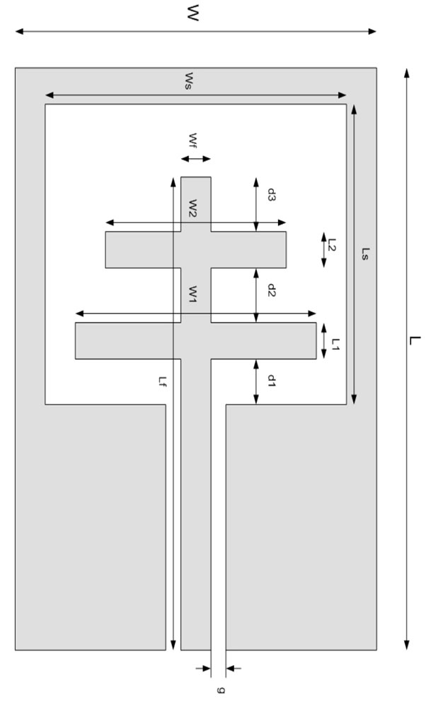
Figure 1. Geometry of proposed antenna.
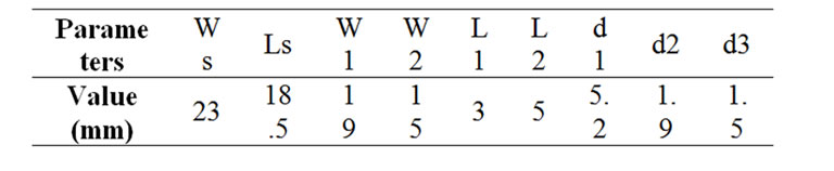
Table 1. Double T-shaped antenna dimensions.
of EBG structures is to exhibit band gap feature in the suppression of surface-wave propagation. Electromagnetic band gap (EBG) structures show the characteristics of forbidding the propagation of electromagnetic waves in certain frequency range and this has been applied in antenna designs [11]. One of the applications is to reduce the mutual coupling between antennas [12], in which the EBG structure is put between two antenna elements and a much higher isolation is obtained.
In this paper, we propose a novel CPW-fed double T-Shaped antenna with simple structure and compact size. These antennas can be tuned to cover the 2.4/5.2 GHz WLAN bands. A multi feed 2-element planar antenna array with the same size is placed on a 78mm × 28.5mm substrate whose thickness is 0.5 mm and dielectric constant is 3.38.We also explore the effect of the proposed planar EBG structure in the mutual coupling reduction and suppression surface-wave between antenna arrays. The mutual coupling between adjacent elements with and without the EBG structure is simulated and compared.
2. Antenna Geometry
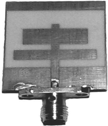
The geometry and parameters of the antenna with double T-shaped stub are shown in Figure 1. The antenna is etched on Rogers RO4003 substrate with a thickness of 20 mil (0.5 mm) and dielectric constant of 3.38. The size of the ground plane is W= 23.5mm × L=28.5 mm. The slot has a length Ls = 18.5 mm and width Ws = 23 mm.
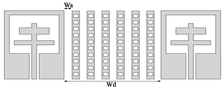
Figure 2. Geometry of EBG structure for coupling reduction.
 (a)
(a)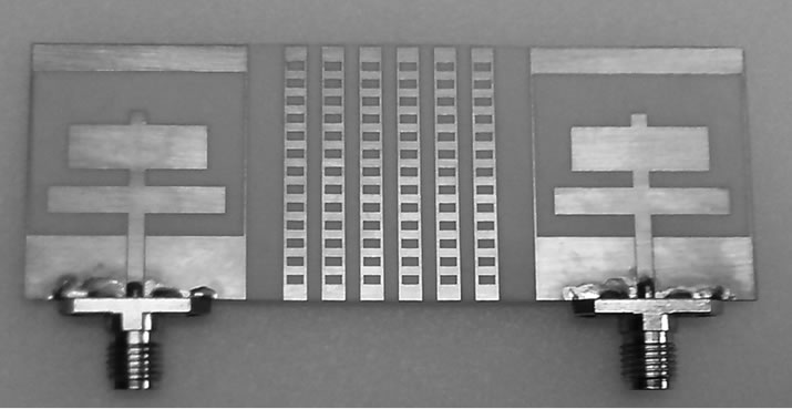 (b)
(b)
Figure 3. Photograph of the antennas a) Single antenna b) Array antenna using EBG.
Table 2. EBG structure dimensions for Double T-shaped antenna.
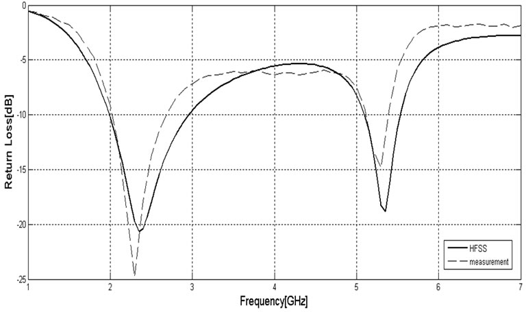
Figure 4. Simulated and measured return loss of the proposed antenna.
The antenna is excited by a 50Ω microstrip line with double T-shaped tuning stub. The width of the 50 Ω microstrip line is Wf =1.75 mm and the gap of the CPW line is g=0.1 mm. The double T-shaped tuning stub is located at the center of the slot, where the antenna is symmetrical along the center, x-axis. Detail dimensions and location of the T-shaped tuning stubs are d1= 2.5mm, d2=1.9mm, d3=1.5mm, L1=3mm, L2=5mm, W1=19mm and W2=15mm. A series of typical dimensions are presented in Table 1.
The proposed planar EBG structure with its geometrical parameters and the geometry of multi-feed 2-element planar antenna array is shown in Figure 2, the size of array is 78mm × 28.5mm, is placed on a substrate whose thickness is 20 mil (0.5 mm) and dielectric constant is 3.38, the distances between the adjacent elements are 31mm, is smaller than quarter wavelength.
The dimension of the EBG structure was 23 mm × 28.5 mm. The EBG structure is fabricated on a 0.5mm thick substrate with relative permittivity 3.38. In this case, 6 columns of metal are used, with an equivalent space 1.6mm, and each element of this metal consists of 13 rectangular slots (slits) etched on it. This structure will be low profile, light weighted and cheaper. The planar EBG structure was used in between a two-element planar antenna array to study its effect on antenna mutual coupling and surface wave. In fabrication, the distance between the antenna and the EBG surface is 4 mm. These dimensions are obtained after performing and optimization. The dimensions of EBG structure are presented in Table 2.
The photograph of the fabricated single and array antenna with EBG structure is shown in Figure 3.
3. Results
The antenna performance was investigated by simulation via HFSS software. Figure 4 shows the measured and simulated return losses of the proposed antenna.
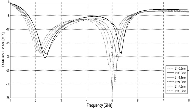
Figure 5. The effect on return loss due to the change of L2.
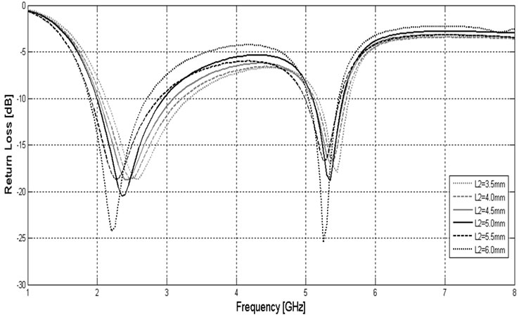
Figure 6. The effect on return loss due to the change of L2.
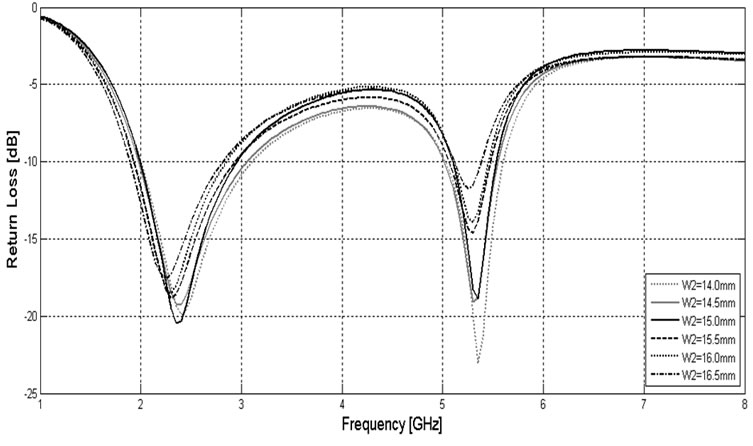
Figure 7. The effect on return loss due to the change of W2.
 (a)
(a)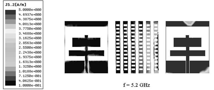 (b)
(b)
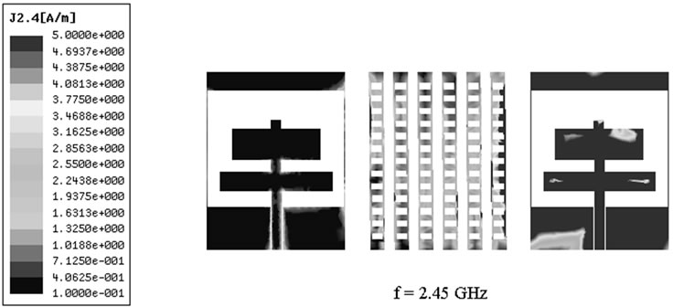
Figure 8. Electric current distribution over the substrate surface a) 2.45 GHz b) 5.2 GHz.
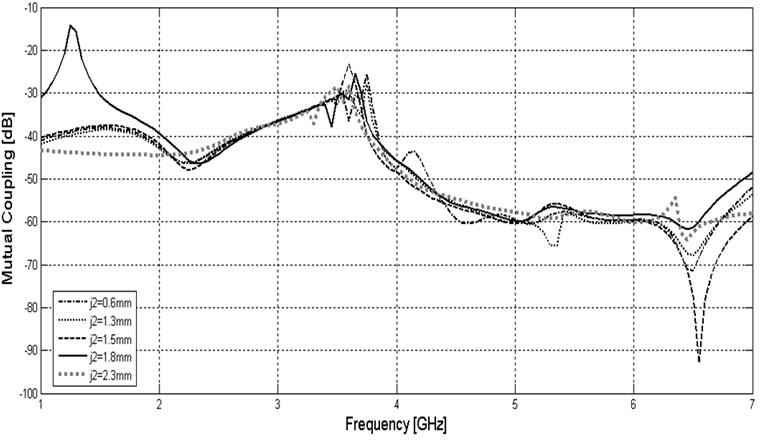
Figure 9. The effect on coupling due to the change of j2.
The obtained -10 dB return loss are 600 MHz (2.05– 2.65GHz) and 500 MHz (5.1–5.4GHz), corresponding to an impedance bandwidth of 25.5% and 5.7 % with respect to the appropriate resonant frequencies. Obviously, the achieved bandwidths can cover the WLAN standards in the 2.4 GHz (2.4–2.484 GHz), 5.2 GHz (5.15–5.35 GHz)
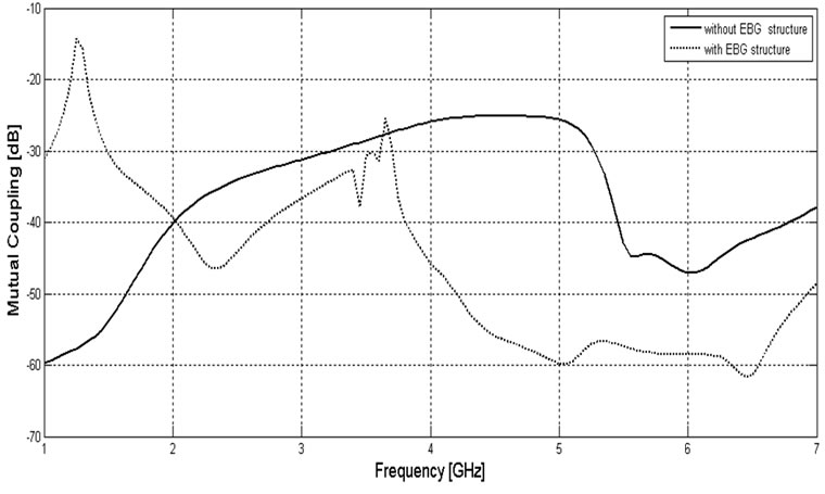
Figure 10. Mutual coupling with and without EBG structure.
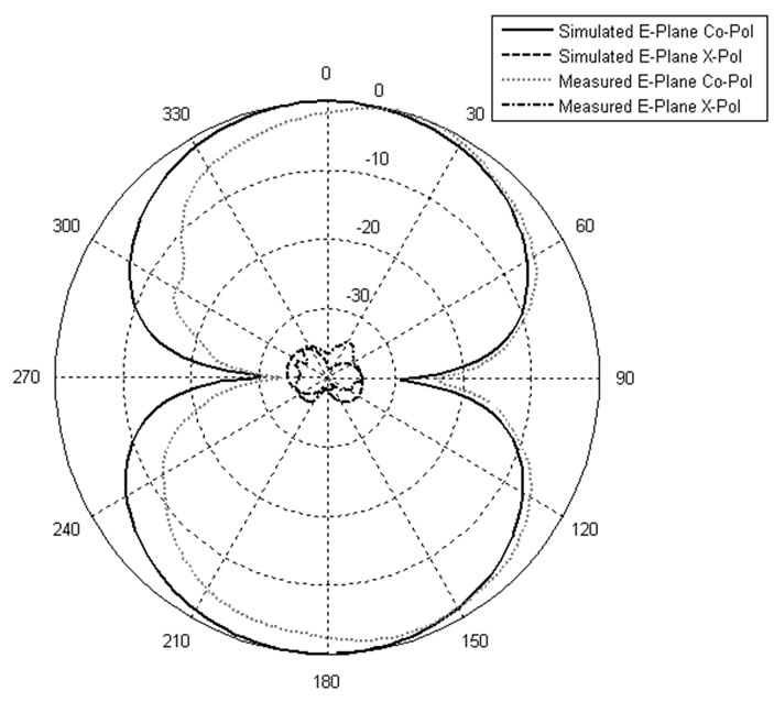
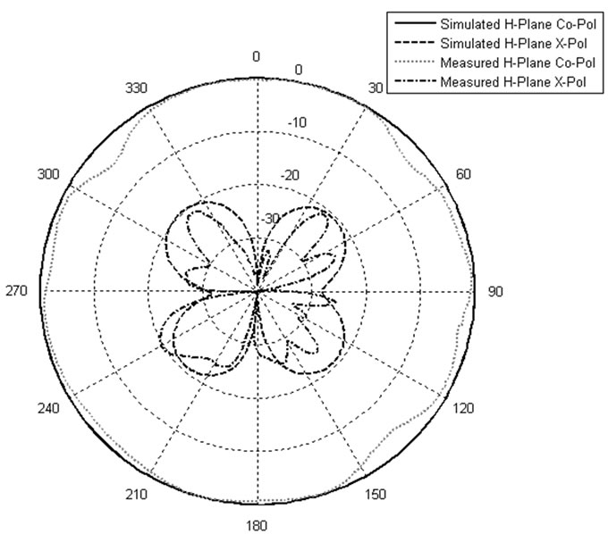
Figure 11. Radiation patterns of proposed antenna at 2.45 GHz.
and 5.8 (5.725–5.825) GHz bands.
In order to provide design criteria for this antenna, the effects of each geometrical parameter are analyzed. The antenna dimensions (L1, L2 and W2) and one parameter are changed at a time while the others are kept constant. Figure 5 to Figure 7 shows the effect of changing L1, L2 and W2, respectively.
In order to reduce coupling, an EBG structure is incorporated between two antennas. It is observed that the EBG structure demonstrates a band stop characteristic, which is enough to thoroughly eliminate the high order mode. The EBG structure not only successfully suppresses higher order modes, but also increases the impedance bandwidth. The planar EBG dimensions (j1 and j2) are chosen to be (1 and 1.5 mm), respectively, and one parameter is changed at a time while the others are kept constant.
Figure 8 shows the HFSS simulated current distributions of the 2*1 array antenna at 2.45, 5.2, GHz with EBG structures. EBG structures acts like a LC filter which rejects any undesired frequency range. This behavior is more studied in Figure 8. The electric current distribution over the substrate is plotted in presence of the EBG structures. Perusing currents distribution, it can be understood that with EBG structure, we decrease current distribution and reduce antenna’s coupling.
Figure 9 shows the effect of changing j2. The rectangular slits etched in the metal are basically used to
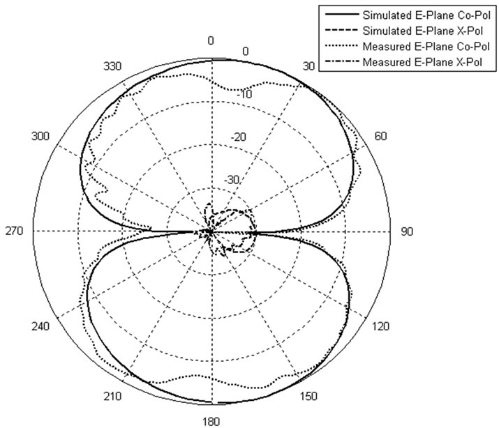
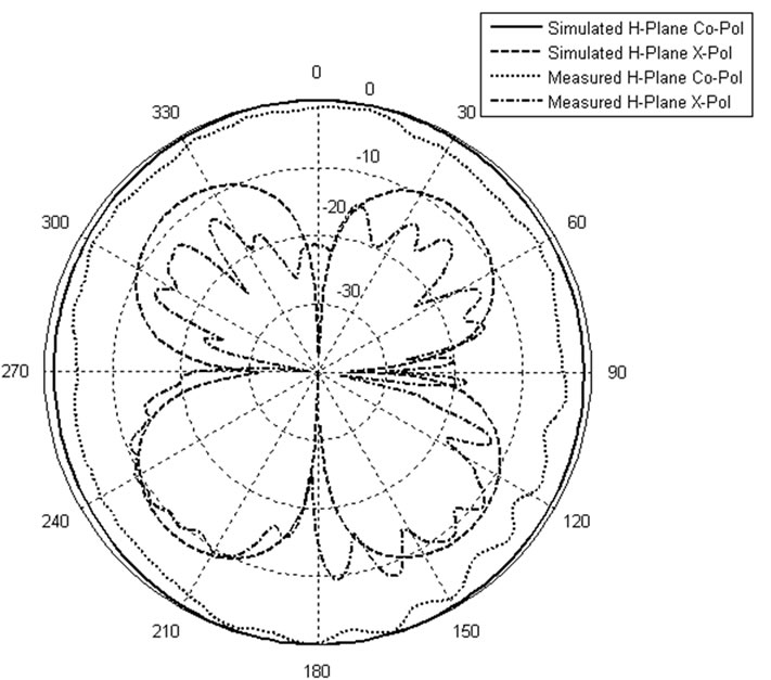
Figure 12: Radiation patterns of proposed antenna at 5.2 GHz.
reduce mutual coupling between radiating elements, therefore the length of 1mm and width of 1.8 mm for slits in the metal is given best result of S12 with -46 dB and -58dB at 2.4 and 5.2 GHz.
The mutual coupling for the antenna arrays with and without the EBG structure is shown in Figure 10. It is evident that the proposed EBG structure can help achieve a significantly low level of mutual coupling. Measured mutual coupling (S21) with EBG structure are -46 dB and -58dB at 2.4 and 5.2 GHz. In addition, measured mutual coupling (S21) without EBG structure are -34 dB and -27dB at 2.4 and 5.2 GHz, (respectively.) This proves that the surface wave is suppressed.
The generation of surface waves decreases the antenna efficiency and degrades the antenna pattern. Since the EBG structure has already demonstrated its ability to suppress surface waves, the planar EBG structures are inserted between antenna arrays to reduce the mutual coupling.
The radiation characteristics of the proposed antenna have also been studied. Figure 11 to Figure 12 show the measured radiation patterns for the E and H-plane pattern including both Coand Cross-polarization at 2.45 and 5.2 GHz for the proposed antenna.
4. Conclusions
A CPW-fed antenna with double T-shaped stub has been proposed for the 2.4/5.2 GHz dual-band WLAN operations. The antenna has characteristics of compact size, a simple structure, good omni directionality and the multi-feed 2-element planar antenna array formed with the compact CPW-fed antennas has satisfied input return loss bandwidth and good radiation patterns. In addition, a prototype of the EBG structure along with an array of two element antenna were fabricated and tested. The EBG structure is inserted between the antenna elements to reduce the mutual coupling and surface wave suppression. Therefore, it is an ideal option for MIMO applications in compact portable devices.
The measured impedance bandwidths are 25.5% at the lower frequency band of 2.4 GHz and 5.7% at the upper frequency band of 5 GHz for the desired bands.
5. References
[1] Y. L. Kuo and K. L. Wong, “Printed double-T monopole antenna for 2.4/5.2 GHz dual-band WLAN operations,” IEEE Transactions on Antennas and Propagation, Vol. 51, No. 9, September 2003.
[2] L. Zhang, Y. C. Jiao, G. Zhao, Y. Song, and F. S. Zhang, “Broadband dual-band CPW-Fed closed rectangular ring monopole antenna with a vertical strip for WLAN operation,” Microwave and Optical Technology Letters, Vol. 50, No. 7, pp. 1929–1931, 2008.
[3] C. M. Wu, “Dual-band CPW-fed cross-slot monopole antenna for WLAN operation,” IET Microwave and Antennas Propagation. Vol. 1, No. 2, pp. 542–546, 2007.
[4] W. C. Liu, “Broadband dual-frequency CPW-fed antenna with a cross shaped feeding line for WLAN application,” Microwave and Optical Technology Letters, Vol. 49, No. 7, pp. 1739–1744, 2007.
[5] Y. Y. Cui, Y. Q. Sun, H. C. Yang, and C. L. Ruan, “A new triple-band CPW-fed monopole antenna for WLAN and WiMAX applications,” Progress in Electromagnetics Research M, Vol. 2, pp. 141–151, 2008.
[6] C. W. Liu, “Optimal design of dual band CPW-fed G-shaped monopole antenna for WLAN application,” Progress in Electromagnetics Research, PIER 74, pp. 21–38, 2007.
[7] W. Ren, “Compact dual-band slot antenna for 2.4/5 GHz WLAN applications,” Progress in Electromagnetics Research B, Vol. 8, pp. 319–327, 2008.
[8] E. Wang, J. Zheng, and Y. Liu, “A novel dual-band patch antenna for WLAN communication,”Progress in Electromagnetics Research C, Vol. 6, pp. 93–102, 2009.
[9] R. Zaker, C. Ghobadi, and J. Nourinia, “A modified microstrip-fed two-step tapered monopole antenna for UWB and WLAN applications,” Progress in Electro-magnetics Research, PIER 77, pp. 137–148, 2007.
[10] R. D. Murch and K. B. Letaief, “Antenna systems for broadband wireless access,” IEEE Communication Magzine, Vol. 40, No. 4, pp. 76–83, April, 2002.
[11] F. Yang and Y. Rahmat-Samii, “Microstrip antennas integrated with electromagnetic band-gap (EBG) struc-tures: A low mutual coupling design for array appli-cations,” IEEE Transactions Microwave Theory Tech-niques, Vol. 51, pp. 2936–2946, October, 2003.
[12] H. K. Xin, M. K. Matsugatani, J. Hacker, J. A. Higgins, M. Rosker, and M. Tanaka, “Mutual coupling reduction of low profile monopole antennas on high-impedance ground plane,” Electronics Letters, Vol. 38, No. 16, pp. 849–850, August, 2002.
NOTES
*Corresponding author