Materials Sciences and Applications
Vol.4 No.9(2013), Article ID:36871,6 pages DOI:10.4236/msa.2013.49070
Palladium Ultra Thin Layer Profiles Evaluation by Evanescent Light
![]()
Holon Institute of Technology, Electrical Engineering Department, Photonics Laboratory, Holon, Israel.
Email: nina.mirchin@gmail.com
Copyright © 2013 Nina Mirchin et al. This is an open access article distributed under the Creative Commons Attribution License, which permits unrestricted use, distribution, and reproduction in any medium, provided the original work is properly cited.
Received June 2619th, 2013; revised July 28th, 2013; accepted August 19th, 2013
Keywords: Pd Nanometer Layers; Evanescent Field
ABSTRACT
Nanometric profiles of sputtered ultra-thin Pd layers with thicknesses in the range 1 - 10 nm were investigated by capturing the leaking evanescent light from optical waveguides. The Pd films were deposited by sputtering on glass substrates also serving as light waveguides. Calibrating the thickness values for the ultra-thin Pd films obtained from the sputtering rate combined with the DELI estimation technique, gave detailed 1D and 3D morphological nanometric profiles of the deposited layers.
1. Introduction
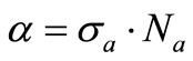
In this work we used the optical microscopy technique named Differential Evanescent Light Intensity (DELI) to investigate nanostructures profiles of Pd sputtered thin films in the ultra-thin thickness range of 1 - 10 nm [1]. DELI is an optical evanescent waves microscopy technique based on capturing the light extracted by nano layers deposited on a substrate which also serves as a waveguide [2,3].
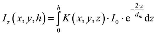
The DELI technique used in this investigation is a far field optical microscopy measurement technique developed to achieve a high resolution for nanometer profiles investigations albeit only into the depth, i.e., z-direction of the samples surface [1-4]. The technique is based on the phenomenon of Total Internal Reflection (TIR) [5,6] at interfaces where evanescent waves occur. This technique has the advantage that the far field image does not include external transmitted or reflected light beams. In fact we rely on the “evanescent light extraction power” of the nanoparticles and nanolayers deposited on a substrate which also serves as an optical waveguide. The TIR phenomenon occurs when light passes from an optically denser medium with refractive index n1 which is the waveguide, into a less denser medium with n2 such as air. The depth, z-axis light beam evanescent intensity variation in the vicinity of the boundary interface between the two media is given by [5,6]:
 (1)
(1)
where the evanescent characteristic “penetration depth” d into the air above the waveguide is defined by [5,6]:
 (2)
(2)
λvac is the vacuum wavelength of the light beam used in the waveguide,  is the critical TIR angle and
  is the angle of light beam incidence upon the waveguide surface. Thus for example, the characteristic penetration depth of the evanescent field for
  from a glass waveguide with n1 = 1.5 into the air is d = 79 nm.
The DELI technique provides an excellent contrast for the layer optical emissivity vs. dark background, enabling nanometer thickness z-profiling by a simple optical densitometry technique, as compared to SEM or TEM microscopy which requires vacuum chambers. The DELI morphology observation technique is also much easier, non destructive, usable in air and more economical for nanometer films profiling as compared to Electron Microscopy or even Atomic Force Microscopy (AFM) since it is better suited also for morphology mapping of large areas as required in industrial applications.
The morphology of the nano-structures observed by DELI in this work with high z-axis resolution sensitivity (thickness) gives 3D and 1D profiles of Pd nanofilms in the extremely low thickness range of 1 - 10 nm.
2. Deposition Experimental Procedure
For PD nanolayers deposition, a sputtering system run at a vacuum of 1 mTorr was employed, and the mean deposited thickness , was calculated according to a calibrated procedure by Equation (3):
 (3)
(3)
where Km is the Pd calibration material constant, Ip is the plasma current, V is the voltage applied and t is the deposition time.
A 10-mm stripe width aperture mask was positioned on top of the glass deposition substrates to obtain 6 stripe areas with various thicknesses in the range of 1 - 10 nm. The glass substrates used were borosilicate microscope slides with dimensions of 75 × 25 × 1 mm. Km was 0.17 × 10⁻¹⁰ when I was measured in mA, V in kV, t in seconds and  in nanometers. The source material was Pd of 99% purity and the sputtering rate used was typically 0.255 nm/s.
3. Nanometer Pd Films Profile Evaluation by DELI
The Pd stripe thin films profiles on the glass surface were observed directly by an optical microscope [1-4], obtaining characteristic parameters of the evanescent field via the DELI phemenological model [1-4]. The visible imaging light beam in the spectral region of (400 - 800) nm coupled into the waveguide was supplied by a GE-Thorn, Quartz Halogen lamp, model DDL, in a fiber illuminator, type Volpi AG, with an integrated output light intensity of I0 = 3.75 W/cm2 at the fiber slit type tip. The evanescent emanating light from the material deposited on the waveguide upper side was captured by a microscope, type Leica Wild M3Z equipped with a CCD camera, with a peak spectral responsivity at 555 nm enabling magnifications of ×(65 - 400).
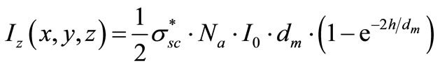
The 2D optical density images were captured by the microscope camera and processed by Computer Image Processing techniques to be displayed finally by 3D perspective images as shown in Figure 1 for 2 typical Pd samples with different average thicknesses. In Figure 2, 6 typical 2D square area sampled images of Pd nanolayers and their mean typical 1D thickness profiles are shown. For each sample, the 2D image of the deposited film has a gray value spatial variance D(x,y) which can be related to the evanescent light intensity I(x,y) captured by the camera, which approximately follows the nanometer thickness profile variation, (z-axis direction) over the deposited area. In Figure 2 below the 2D square zone images with areas of (520 × 520) µm2 the 1D x-direction thickness profiles of the 2D areas obtained by averaging over the y-coordinate are shown for the 6 nanolayer samples with mean thicknesses in the range of 1 - 10 nm. One may observe that the thickness increases from left to right corresponding to the direct thickness calculation using Equation (3) during the deposition, i.e., the lighter areas have higher thicknesses. The utmost right dark square is the non-deposited zone image.
To evaluate the relative and absolute surface nanoprofiles thicknesses of the various samples in the z-direction, the mean Normalized Integrated Optical Density (NIOD) was measured experimentally from the images of the deposited zones shown in Figure 2, being defined as:
 (4)
(4)
where  is the gray level value of each pixel (0-255), S is the sampled image area and H(D) is the image histogram i.e., the number of pixels per gray level.
To calibrate the NIOD to absolute thicknesses values we used the Pd6 sample with the greatest thickness which was obtained by a sputtering rate of 2.55 nm/s, giving a nominal thickness value of 10 nm. The graph in Figure 3 shows the nanolayer thickness calculated points (asterisks) from DELI evaluation and the solid line from the sputtering deposition Equation (3) vs. time of deposition.
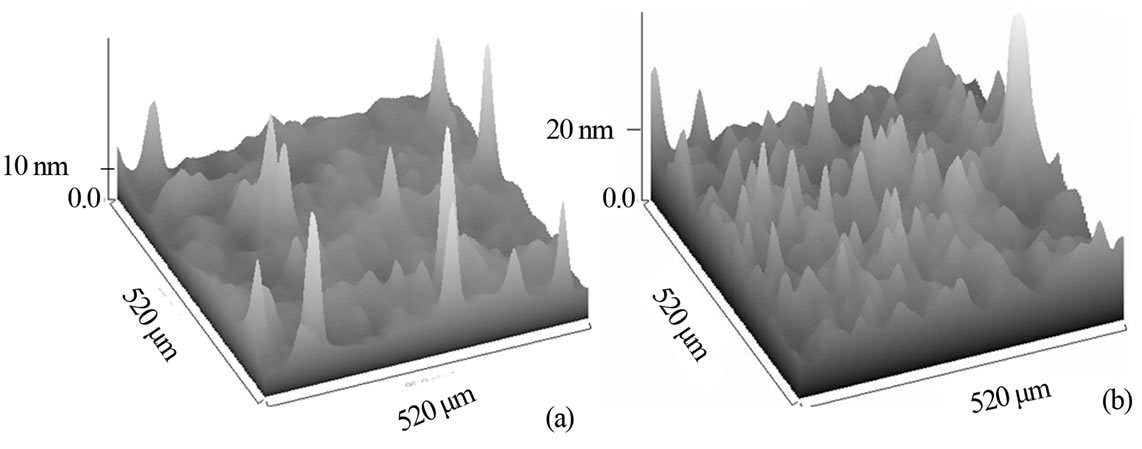
Figure 1. DELI 3D perspective images of a Pd sampled areas of (520 × 520) µm2: with mean thickness of about (a) 4 nm, (b) 10 (nm).
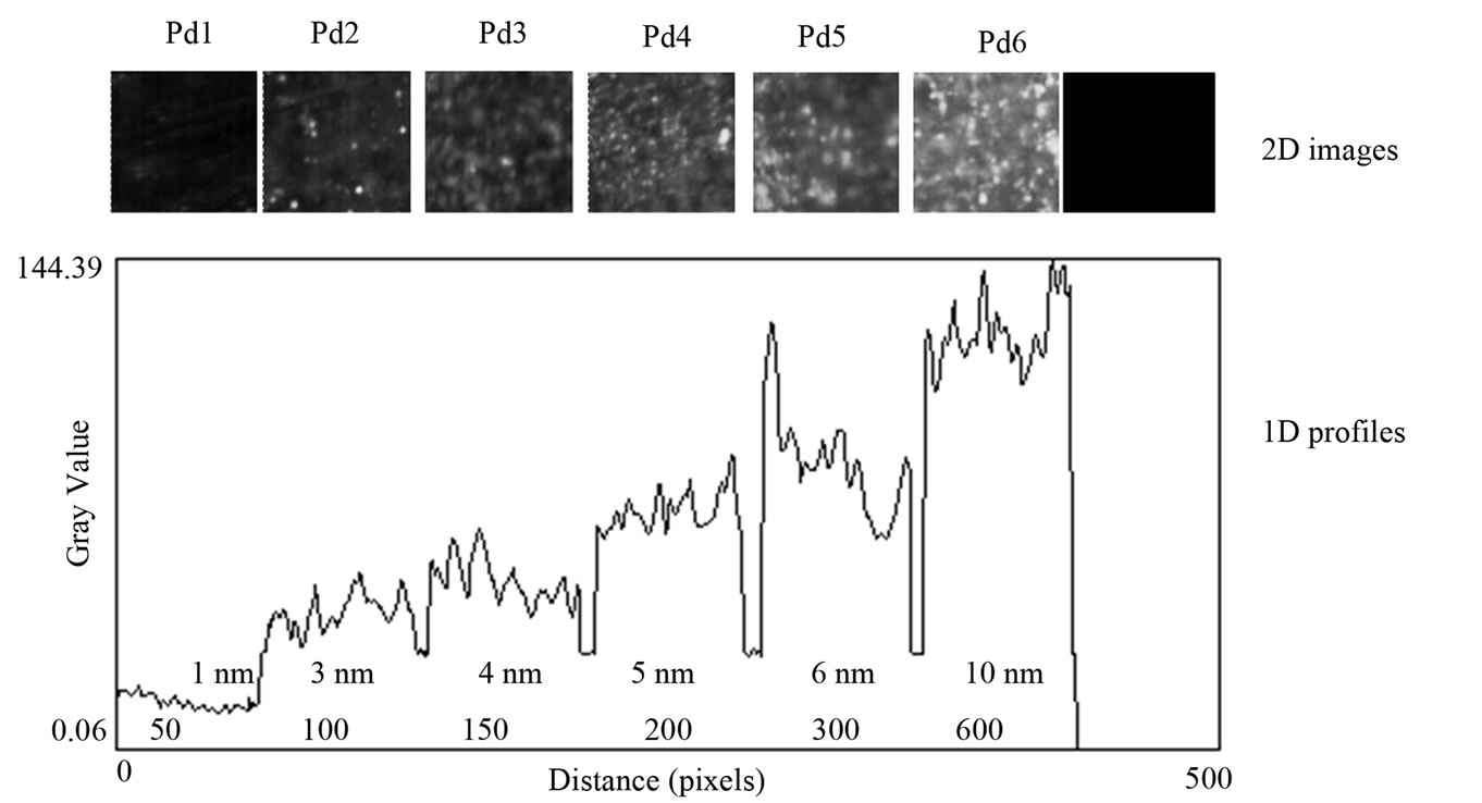
Figure 2. 2D images of 6 Pd sampled areas profiles with thicknesses in the range 1 - 10 nm. Below the 2D images, as captured by the camera at x65 magnification of the microscope, 1D profile plots of the sampled areas are shown. The sampled 2D zones have an area of (520 × 520) µm2. The utmost right black square is the non-deposited zone image.

Figure 3. Plots of the nanolayer thickness vs. time of deposition from DELI evaluation (asterisks) (*) for the measured samples and from the sputtering rate of deposition equation Equation (3) (solid line).
4. DELI Photon Extraction Model
In the DELI technique it is assumed that the evanescent light optical power extracted from the waveguide depends on the volume number density of the deposited nanoparticles on the waveguide surface. In the non-deposited areas, complete TIR occurs for the light propagating inside the waveguide and no light emerges, see utmost right darkest square in Figure 2. However, the nanometer particles deposited on the surface scatter the light of the evanescent waves in proportion to their number density, up to an effective distance from the interface when the photon-material interaction due to regular optical absorption becomes too strong. The evanescent waves measurements enable thus the observation of the spatial depth z-profile of the nanolayer on the waveguide when the optical absorption of the nanolayer is very small.
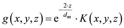
In our experiments we used the evanescent wave extraction power of the Pd nanomaterial deposited on the glass substrate to obtain its 3D profiles and also particular or mean 1D depth profiles. Assuming that the material consists of an aggregate of spherical particles on the waveguide surface and that the evanescent light intensity in the air close to the waveguide is perturbed by the deposited particles and extracted by tunneling or scattering, the evanescent light intensity  arriving at the CCD detector is given formally by [1,2]:
 (5)
(5)
where I0 denotes the optical field intensity at the waveguide/material interface and  is the photon extraction efficiency of the deposited material from the light field propagating within the waveguide at any interface point
 .
.  contains the physical mechanism of the material-photon extraction power depending on the interaction between the evanescent photons and the deposited particles on the waveguide. Assuming a generating model function
  we write for
  :
:
 (6)
(6)
where  is the nanolayer thickness at point
  and the value of
  can be determined experimentally from the
  plane spatial light intensity distribution measured by the microscope camera.
The model generating function , may be derived in principle from an appropriate physical mechanism relating to the photons extraction mechanism from the waveguide. Assuming the evanescent intensity scattering mechanism by the nanoparticles is such that the fractional light scattered intensity from the layer in the z-direction, i.e.,
  is proportional to the evanescent field intensity, we obtain the following differential equation describing the scattered evanescent field intensity at the camera:
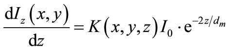 (7)
(7)
Here,  denotes the evanescent field intensity which is an exponentially decreasing function in the z-direction [5,6]. I0 denotes the optical field intensity at the waveguide/material interface and
  is a parameter containing the physical mechanism by which the nano-structured material deposited on the substrate extracts the evanescent photons from the waveguide, e.g., tunnelling, scattering and fluorescence. The parameter
  defined in Equation (7), differs from d given in Equation (2), and represents a characteristic penetration depth of the evanescent field into the nanomaterial deposited above the waveguide [5,6].
By integrating Equation (7) in the z direction, through the nanolayer thickness from 0 to  at point
  one obtains:
 (8)
(8)
Comparing the integrand in Equation (8) with the definition of the phemenological model function  we obtain the following relations:

and
For a simple linear light scattering mechanism from the deposited particles we can write for :
:
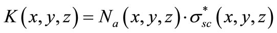 (9)
(9)
where 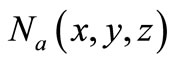 is the nanoparticles concentration in
(cm–3) and  is the evanescent scattering cross
section of the particles in (cm2).
For the simple case of constant particles volume concentration Na and evanescent cross section  the integration of Equation (8) using (9) gives:
 (10)
(10)
Consequently, the normalized light intensity spatial distribution which is the optical response of the CCD camera measuring the evanescent scattered light intensity has the form:
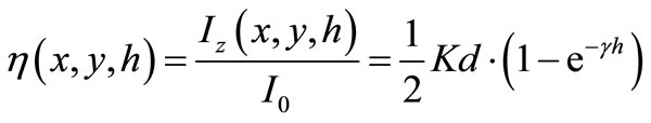
With
 (11)
(11)
We note that in Equation (11) the parameter  is an “effective” depth value related to the interaction range of the evanescent field with the nanoparticles deposited on the waveguide.
From Equation (11) we obtain at two points  with
with  with two different thicknesses h1,h2 the
 :
:
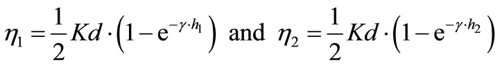 (12)
(12)
We showed in [2] that the NIOD of Equation (4) is approximately proportional to the average thickness of the imaged zone and also to , hence using Equation (12) one obtains the following ratio for the NIODi’s and
  :
:
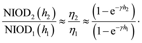 (13)
(13)
For absolute thicknesses calculation, rather than using relative thicknesses values, h1 or h2 can be calibrated by independent techniques such as spectrometry, SEM, AFM or mechanical nanoprofilometry. In this way, absolute values for thickness  spatial profiles can be derived from the experimental NIOD values and if
  is known [1-4]. Also, given the absolute thickness value of h2 one can calculate other thicknesses hi of the nanoprofile from Equation (13).
5. Results
The “effective” penetration depth parameter  was determined experimentally as follows: A parameter k is defined as:
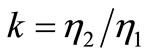 (14)
(14)
For any two points with thicknesses  and for k > 1, using Equation (12) with a tolerance set at
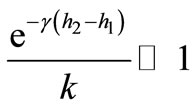 we obtain:
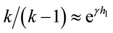 (15)
(15)
Then, the following estimation for the  value can be obtained from Equation (15) using the experimental ratio k in Equation (15) by:
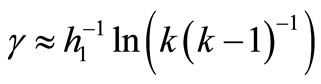 (16)
(16)
For the Pd nanolayers investigated in this work, the ![]() mean experimental value obtained using Equation (16) from Figure 2 is given in the first row and column in Table 1, together with additional parameters related to Pd and other materials i.e., In and a-Au investigated previously [4]. In the second row, the effective penetration depth dm approximated by
mean experimental value obtained using Equation (16) from Figure 2 is given in the first row and column in Table 1, together with additional parameters related to Pd and other materials i.e., In and a-Au investigated previously [4]. In the second row, the effective penetration depth dm approximated by  is given.
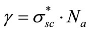
Regarding the mechanism of the evanescent wave extraction, many authors [5,6,10-13] assume that the molecules dipoles deposited on the planar interface are responsible for the evanescent photons scattered from the deposited layers. The maximum number of dipole molecules per unit volume Na can be estimated by the following equation [14]:
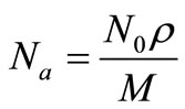 (17)
(17)
where N0 = 6.022 × 10²³ [atoms/mol] is the Avogadro number,  is the material density in [g/cm3] , and M is the molecular mass in [g/mol]. The material density
  and molecular mass M of Pd as well as the results obtained from Equation (17) for the number of molecules per unit volume Na are given in Table 1.
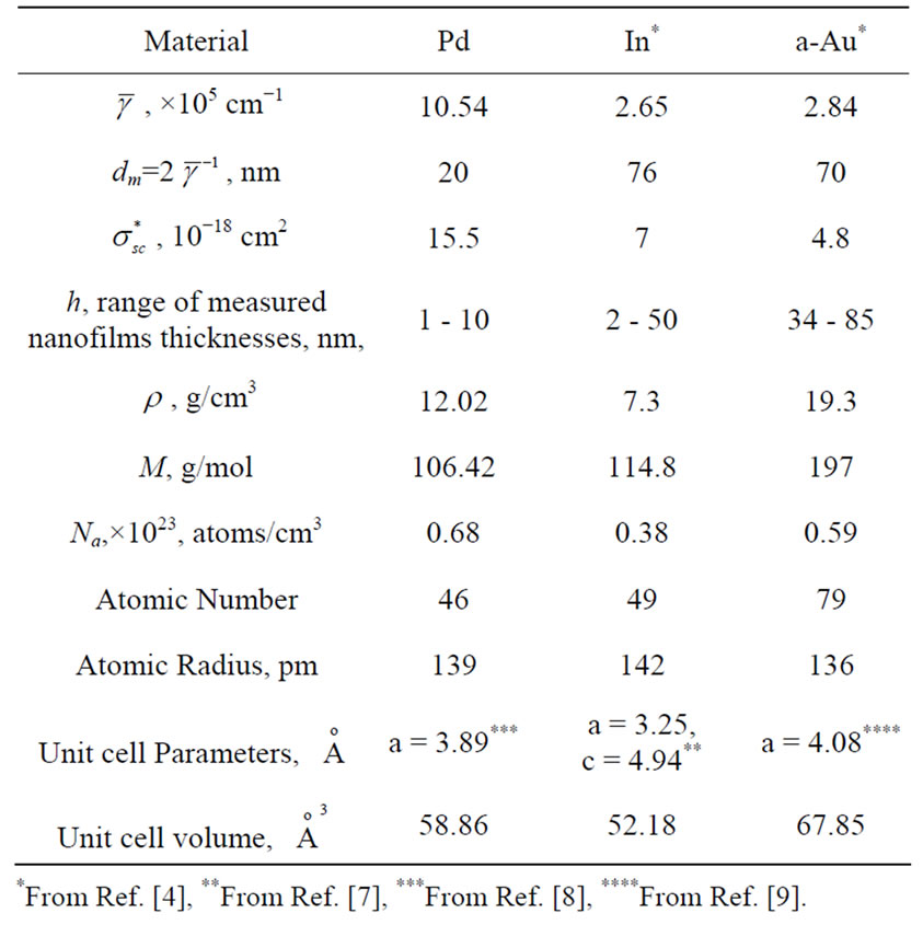
Table 1. Evanescent photon extraction parameter , the material density
 ![]() in [g/cm3] , the molecular mass M in [g/mol], maximum number of molecules per unit volume Na , effective scattering cross-section
in [g/cm3] , the molecular mass M in [g/mol], maximum number of molecules per unit volume Na , effective scattering cross-section  for Pd in this work, and for a-Au and In from Ref. [4].
*From Ref. [4], **From Ref. [7], ***From Ref. [8], ****From Ref. [9].
The material optical absorption coefficient ![]() is usually related to the absorption cross-section
is usually related to the absorption cross-section  and the concentration of the light absorbing particles Na by the following equation:
 (18)
(18)
Similarly  can be described also as a product of an effective scattering cross-section
  of a volume concentration
  of light scattering dipoles by:
 (19)
(19)
Thus, using Equation (19) and the number density of molecule dipoles per unit volume from Equation (17), can provide an estimation for the “effective” evanescent scattering cross-section  of the nanometer particles for the Pd nanaolayers as given in Table 1. Comparing (19) with (9), we observe that
 is a function of K and the experimentally obtained
 ![]() given in Table 1 is the mean value averaged over the area S and thickness h :
given in Table 1 is the mean value averaged over the area S and thickness h :

6. Discussion
It is of interest to compare the results obtained for Pd with the previous results for other metals such as a-Au and Indium [4]. The specific gravity and atomic masses for a-Au, Indium, and Pd as well as the results obtained from Equation (17) for the number of atoms per unit volume are given in Table 1. As seen in Table 1, the number of molecules per unit volume Na increases from In to a-Au and Pd as does , thus the number of excited dipoles assumed in the dipole scattering model is approximately proportional to the molecules volume density of the material deposited [11-13]. However, we observe that the “effective” scattering cross-section,
  , does not follow the
  monotonic increase with Na but rather decreases monotonically with the materials molecular weight M. Thus while a higher
  value suggests a greater graininess of the material aggregation structure on the surface,
  relates to the higher intrinsic evanescent cross section for materials with lower molecular mass.
7. Conclusions
We used the nanometer optical profile diagnostic method DELI [1-4] to obtain the “mean effective” evanescent light extraction parameter ![]() of the Pd nanolayers deposited by sputtering. The results were compared with previous data on a-Au and Indium, showing the particular dependences of the “effective” extraction depth evanescent parameter
of the Pd nanolayers deposited by sputtering. The results were compared with previous data on a-Au and Indium, showing the particular dependences of the “effective” extraction depth evanescent parameter 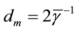 on the number of dipole molecules per unit volume Na and the scattering cross section
  with the molecular weight M.
The DELI z-profiling optical microscopy method proved highly sensitive enabling the observation of Pd nanofilms thickness profiles variations in the range of 1 - 10 nm, providing at the same time information about the evanescent cross section dependence of the evanescent scattering by the nanoparticles.
REFERENCES
- G. Socol, E. Axente, M. Oane, L. Voicu, A. Petris, V. Vlad, I. N. Mihailescu, N. Mirchin, R. Margolin, D. Naot and A. Peled, “Nanoscopic Photodeposited Structures Analyzed by an Evanescent Optical Method,” Applied Surface Science, Vol. 253, No. 15, 2007, pp. 6535-6538. doi:10.1016/j.apsusc.2007.01.076
- N. Mirchin, M. Gankin, U. Gorodetsky, S.A. Popescu, I. Lapsker, A. Peled, L. Duta, G. Dorcioman, A. Popescu and I. N. Mihailescu, “Estimation of Polyethylene Nanothin Layer Morphology by Differential Evanescent Light Intensity Imaging,” Journal of Nanophotonics, Vol. 4, No. 1, 2010, Article ID: 014760.
- N. Mirchin, B. Apter, I. Lapsker, V. Fogel, U. Gorodetsky, S. A. Popescu, A. Peled, G. Popescu-Pelin, G. Dorcioman, L. Duta, A. Popescu and I. N. Mihailescu, “Measuring Nanolayer Profiles of Various Materials by Evanescent Light Technique,” Journal of Nanoscience and Nantechnology, Vol. 12, No. 3, 2012, pp. 2668-2671. doi:10.1166/jnn.2012.5788
- N. Mirchin and A. Peled, “Evaluating Nanoprofiles of Materials Deposited on Waveguides by an Evanescent Light Method,” Journal of Advanced Microscopy Research, Vol. 7, No. 1, 2012, pp. 1-6.
- L. Novotny and B. Hecht, “Principles of Nanooptics,” Cambridge University Press, Cambridge, 2006.
- F. de Fornel, “Evanescent Waves from: From Newtonian Optics to Atomic Optics,” Springer Series in Optical Sciences, Vol. 73, Springer Verlag, Berlin, 2000.
- http://www.mindat.org/min-2030.html
- http://www.periodni.com/pd.html
- http://webmineral.com/data/Gold.shtml
- C. Girard, “Near Fields in Nanostructures,” Reports on Progress in Physics, Vol. 68, No. 8, 2005, pp. 1883-1933. doi:10.1088/0034-4885/68/8/R05
- E. Eremina, N. Grishina, Y. Eremin, L. Helden and T. Wriedt, “Total Internal Reflection Microscopy with a Multilayered Interface: A Light Scattering Model Based on a Discrete Sources Method,” Journal of Optics A: Pure and Applied Optics, Vol. 8, No. 11, 2006, pp. 999-1006. doi:10.1088/1464-4258/8/11/011
- M. Quinten, A. Pack and R. Wannemacher, “Scattering and Extinction of Evanescent Waves by Small Particles,” Applied Physics B, Vol. 68, No. 1, 1999, pp. 87-92. doi:10.1007/s003400050591
- G. P. Wiederrecht, “Near Field Optical Imaging of Noble Metal Nanoparticles,” The European Physical Journal— Applied Physics, Vol. 28, No. 1, 2004, pp. 3-18. doi:10.1051/epjap:2004170
- R. E. Hummel, “Electronic Properties of Materials,” 3rd Editon, Springer-Verlag, New York, 2001, p. 204. doi:10.1007/978-3-642-86538-1