Wireless Engineering and Technology
Vol.2 No.3(2011), Article ID:5831,8 pages DOI:10.4236/wet.2011.23027
A Versatile Industrial Timer and Real Time Keeper
![]()
Electronics and Communication Engineering Department, Amrita School of Engineering, Coimbatore, India.
Email: sagar.g.y@gmail.com, ka_narayanankutty@cb.amrita.edu
Received February 10th, 2011; revised March 20th, 2011; accepted April 27th, 2011.
Keywords: Industrial Timer, Real Time Clock, Programmable, Standalone, DS1307, I2C, USART, ZigBee, Bluetooth
ABSTRACT
Industrial timer requirements are multifaceted. On-delay, off-delay, cyclic or sequential timing requirements, with usual time range varying from seconds to days, depending on the process. Custom build timers cannot provide all of these requirements simultaneously and hence an advanced timer rectifying this shortcoming has been designed and fabricated in this work. This timer is based on the real time clock chip used in mother boards. Our design can be programmed for a specific time requirement and can later be put to work in standalone mode. A demonstration board is fabricated and tested.
1. Introduction
In this paper we are presenting a unique gadget that ensures the timely operation of a device under control. The gadget offers accurate timekeeping functionality spanning from seconds to days and different modes of operations. This meets the varying needs of the industries and research laboratories. Easy to configure via the RS232 interface, the gadget doesn’t require any drivers or specialised application softwares for interfacing it with the PC. The gadget could be powered from the USB port of the PC while configuring, thereby eliminating the need for an external power supply. This USB port also interfaces the driver circuit to it. The driver circuit is used to drive the device under control.
Many Industrial Timers are available in the market from leading manufacturers like the 405 Series Industrial Timers with ON Delay/Interval Timing mode of operations [1], the 407 Series Multi mode Industrial Timers with ON Delay/OFF Delay/Interval Timing mode of operations [2], the RG-21 and GP2 series Cycle Industrial Timers with cyclic mode of operations [3,4]. One of primary difficulty faced while deploying these kinds of industrial Timers is that they don’t offer all the different timing requirements like the Delayed ON/ Delayed OFF or Cyclic simultaneously in one single unit. Moreover they need to be configured manually each time after a cycle of operations and doesn’t offer the possibility of configuring them remotely using wireless links. Remote configuration of these Timers proves very beneficial especially when they are installed in harsh, not easily accessible locations in the industries. The Industrial Timer module described in this paper overcomes all the above mentioned difficulties and shortcomings offered by the units available in the market at present. The gadget offers all the different Industrial timing requirements like ON Delay/OFF Delay/or Cyclic simultaneously and can be configured for 25 Cycles at a go. The gadget is soft configured via RS232 Interface and could be even remotely configured by attaching the gadget to compact ZigBee or Bluetooth Module made to operate in the Transparent Mode. In the transparent mode these RF Modules can replace the Serial (RS232) Port to establish connections between the PC/Base Station and the Timer module.
The gadget has two modes of operation namely: Configuration mode and Standby mode. The two modes of operation could be selected with the help of a Push to ON switch available on the gadget. In the configuration mode the device could be interfaced with the PC via the RS232 port to set the RTC time and to edit the time settings for the device under control. Windows© HyperTerminal can be used to communicate with the gadget in this mode. In the standby mode the gadget will be interfaced with the accompanying driver circuit to drive the device under control. The gadget incorporates a Real Time Clock module that keeps track of the system time. The module has a battery backup provided with the aid of a 3V Li Cell that ensures uninterrupted tracking of system time.
The gadget offers a flexible mode of operations which can be tailored to meet different timekeeping requirements. It can be used to implement a delayed ON/OFF operation of the device or can even be used to execute a periodic sequence of device operation by enabling the looping of time settings.
The paper is organised as follows: Section 2 gives details of the real-time clock chip, how the chip is accessed and used. Section 3 describes details of the circuits and firmware used. Section 4 explains the gadget operation and the configuration details along with screenshots. We conclude this paper with the potential applications of the gadget in Section 5.
2. DS1307 Real Time Clock
DS1307 Serial Real-time Clock is a low power, fully binary-coded decimal (BCD) clock/calendar plus 56 bytes of NV SRAM [5]. Address and data are transferred serially via a 2-wire, bi-directional bus (I2C). The clock/ calendar provides seconds, minutes, hours, day, date, month, and year information. The end of the month date is automatically adjusted for months with fewer than 31 days, including corrections for leap year. The clock operates in either the 24-hour or 12-hour format with AM/PM indicator. The DS1307 has a built-in power sense circuit that detects power failures and automatically switches to the battery supply. The Real-Time Clock circuitry includes a 32.768 KHz quartz crystal that clocks the module. A battery back-up is provided using a 3V Li cell CR2025.
The DS1307 operates as a slave device on the serial bus. Access is obtained by implementing a START condition and providing a device identification code followed by a register address. Subsequent registers can be accessed sequentially until a STOP condition is executed. The information is transferred byte-wise and each receiver acknowledges with a ninth bit. The device that acknowledges pulls down the SDA line during the acknowledge clock pulse. This is depicted in the timing diagram shown in Figure 1. Within the 2-wire bus specifications a regular mode (100 KHz clock rate) and a fast mode (400 KHz clock rate) are defined. The DS1307 operates in the regular mode (100 KHz) only. During data transmission and reception over the I2C bus DS1307 operates in the following two modes:
2.1. Slave Receiver Mode (DS1307 Write Mode)
Serial data and clock are received through SDA and SCL. After each byte is received an acknowledge bit is transmitted. START and STOP conditions are recognized as the beginning and end of a serial transfer. Address recognition is performed by hardware after reception of the slave address and direction bit (Figure 2). The address byte is the first byte received after the start condition is generated by the master. The address byte contains the 7 bit DS1307 address, which is 1101000, followed by the direction bit (R/W) which, for a write, is a 0. After receiving and decoding the address byte the device outputs acknowledge on the SDA line. After the DS1307 acknowledges the slave address + write bit, the master transmits a register address to the DS1307. This will set the register pointer on the DS1307. The master will then begin transmitting each byte of data with the DS1307 acknowledging each byte received. The master will generate a stop condition to terminate the data write.
2.2. Slave Transmitter Mode (DS1307 Read Mode)
The first byte is received and handled as in the slave receiver mode. However, in this mode, the direction bit will indicate that the transfer direction is reversed. Serial data is transmitted on SDA by the DS1307 while the serial clock is input on SCL. START and STOP conditions are recognized as the beginning and end of a serial transfer (Figure 3). The address byte is the first byte received after the start condition is generated by the master. The address byte contains the 7-bit DS1307 address, which is 1101000, followed by the direction bit (R/W) which, for a read, is a 1. After receiving and decoding the address byte the device inputs acknowledge on the SDA line. The DS1307 then begins to transmit data starting with the register address pointed to by the register pointer. If the register pointer is not written to before the initiation of a read mode the first address that is read is the last one stored in the register pointer. The DS1307 must receive a “not acknowledge” to end a read.
3. Circuit and Firmware
The circuit for the gadget could be split into two parts namely: the control circuit and the driver circuit. The control circuit constitutes the complete circuit for the gadget, whereas the driver circuit forms the part of the driver module to which the gadget is interfaced during the standby mode.
3.1. Control Circuit
The complete circuit diagram for the control circuit is shown in Figure 4. The 8-bit microcontroller, AVR Amega8 [6] forms the heart of the control circuit along with the Real time clock form Dallas Semiconductor, DS1307. The microcontroller is clocked at 8 MHz using a quartz crystal Q2, whereas the Real time clock module DS1307 requires a clocking of 32.768 KHz which is also provided using a quartz crystal Q1. The entire circuit is powered using a DC 5V derived through the PC USB
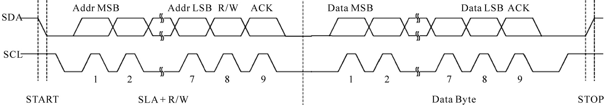
Figure 1. I2C address and data packet format.
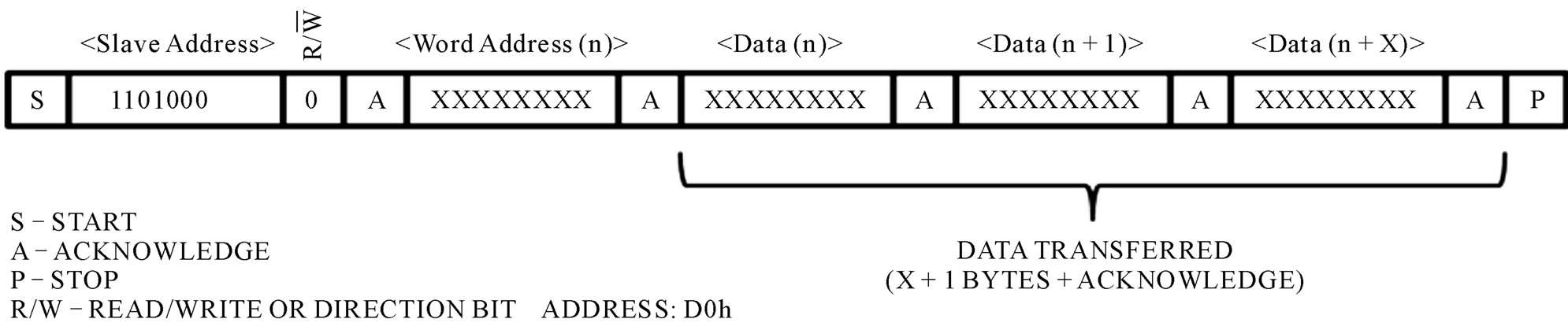
Figure 2. Data write—slave receiver mode bit sequence.
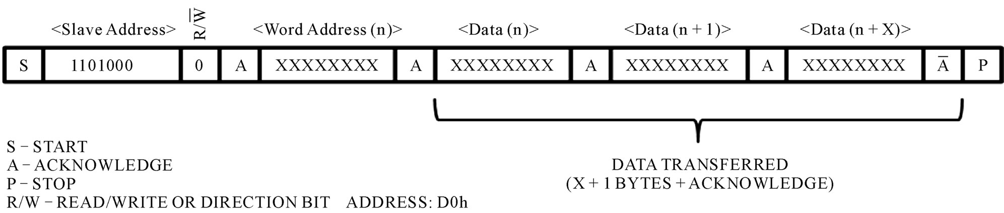
Figure 3. Data read—slave transmitter mode bit sequence.
port. The gadget is connected to the PC for configuration or to the timekeeper driver circuit through the same USB port, when operating in the standby mode. The power derived from the USB port, X1 pins 1 & 4 is filtered using an electrolytic capacitor C1 and is indicated using a power LED, LED1 via a current limiting resistor R1. A power on reset circuit is constructed for the microcontroller using the resistor capacitor network formed by R2 and C9. The controller could also be forced to reset using the tactile switch S2. Push to ON switch S1 connected to pin 13 of the microcontroller is used to set the configuration mode. When the switch is ON the gadget enters into the configuration mode.
In order to interface the gadget with the PC we make use of the USART module available in the microcontroller [7]. We set the USART module to operate in the asynchronous mode at a baud rate of 38400 bps. The frame format is 8 data bit with no parity bit and a stop bit. The RXD and TXD terminals of the USART module from the microcontroller is connected via a level converter circuit to the DB9 female port X2. Since the RS232 signals go between +12V and –12V and are inverted (–12V is a logical 1), applying this kind of voltage to the AVR is dangerous. So MAXIM’s MAX232 [8] level converter is used between the DB9 female serial port and the MCU. The MAX232 uses capacitor pumps to perform the necessary level shifting and provide receive and transmit signals.
The circuit also includes a 6 pin ISP header port, SV1 to facilitate in-circuit serial programming of the microcontroller. Any ISP programmer could easily be interfaced with the gadget through this port to program the microcontroller. The ISP header on-board gives access to MOSI, MISI, SCK and RESET pins of the microcontroller for SPI programming.
The Real-Time Clock circuitry, built around DS1307, keeps track of the system time. The Real-Time Clock circuitry includes a 32.768 KHz quartz crystal, Q1 that clocks the module. A battery back-up provided using a 3V Li cell CR2025, G1. Two pull up resistors R4 and R5 each of 4.7KΩ are used to ensure proper bus conditions on the SCL and SDA lines of the I2C bus [9]. Pull up resistor R3 is used across SQW/OUT pin for its proper operation since it is of open drain type. The SCL and
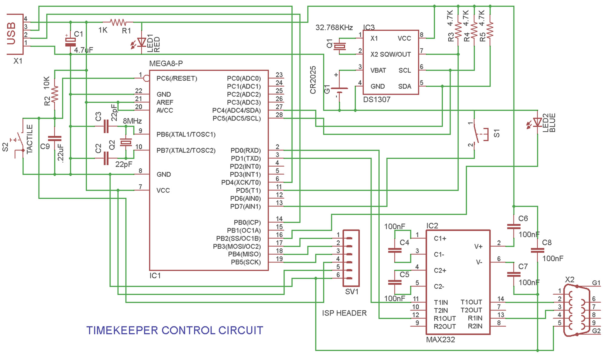
Figure 4. Circuit diagram of the control circuit.
SDA lines from the RTC module are in turn connected to the corresponding bus terminals of the microcontroller to establish the I2C bus. The SQW/OUT connection from the RTC module is connected to T1 pin of microcontroller which forms the external clock source for the internal 16-bit Timer/Counter module available in Atmega 8. A fluorescent blue LED is connected across the OC1B output pin of microcontroller. OC1B forms the output pin of one of the two output-compare units of the 16-bit Timer/Counter module [10]. The LED flashes at a rate of 2 Hz giving a visual indication of the internal time ticking in the gadget.
3.2. Driver Circuit
The complete circuit diagram for the driver circuit is shown in Figure 5. The timekeeper driver circuit could be divided into two main sections namely: Power supply section and the Driver section. The power supply section makes use of a positive voltage regulator LM7805 [11] along with smoothing capacitors C10, C11, C12, and C13 to generate a regulated fixed output voltage of + 5V from a raw DC voltage derived from the DC Power jack. Any DC voltage between +7.5V to +20V could be safely applied through the DC Power jack to power up the circuitry. Diode D1 has been used to protect the circuit from accidental polarity reversal. A red LED, LED4 along with current limiting resistor R6 provides power on indication. The regulated +5V generated by the power supply circuitry is also fed through the USB port, X5 to power up the gadget when interfaced with the driver circuit during standby mode of operation.
The driver circuitry makes use of NPN transistors T1 and T2 as switches to drive the relay and buzzer module respectively. Resistors R7 and R9 ensure the proper biasing condition for the transistors when drive signal appears at USB port pins 2 and 3. Diode D2 is connected across the relay module to bypass the back e.m.f generated and thus protects the remaining circuitry. We have used a 6V PCB mountable relay cube in our prototype. The normally open contact of the relay module is used to connect the device under control to the live AC power. Green LED, LED3 along with current limiting resistor R8 provides a status indication of the relay module and hence the device under control. The LED will light up when the relay is activated. Push to ON switch S4 is used to connect and disconnect the driver circuit for buzzer module from the remaining circuitry, if unwanted.
3.3. Firmware
The firmware for the gadget is written in embedded C and is compiled and debugged using AVR Studio 4. The entire firmware for the microcontroller has been carefully organised into several source files each of which is defined using its corresponding header files. The source file along
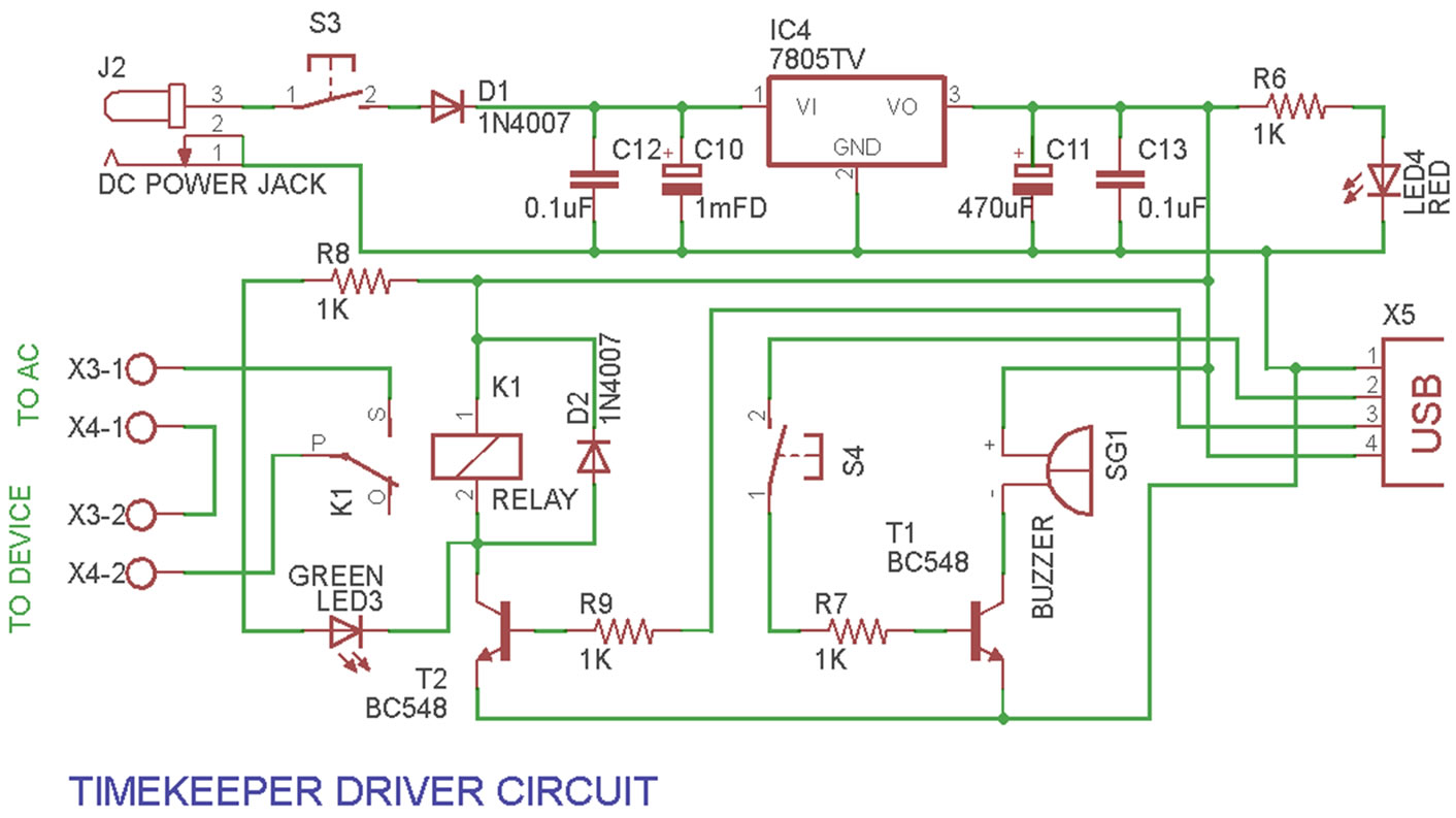
Figure 5. Circuit diagram of the driver circuit.
with the header file takes care of specific applications and includes routines that could be invoked for the same from the main file. Apart from the application specific user defined header files and its corresponding source files the program also includes several other utility and standard header files from the AVR library. For handling EEPROM read-write operations the utility header file eeprom.h has been included in the project from the AVR library [12]. Similarly for generating accurate delays of milliseconds and microseconds the utility header file delay.h is included. A detailed description for the different user defined header files is given in Table 1. Each of the user defined header files accompanies a source file that defines the routines declared in their corresponding header files.
The relevant data and guidelines for programs are taken from references [13-16].
4. Gadget Operation
As mentioned before the gadget has two modes of operation namely: the configuration mode and the standby mode. In the configuration mode, which is selected by pressing switch S1 to ON position, communication could be established with the gadget over the USART bus with the help of HyperTerminal software. In the configuration mode the user can do the following operations:
• Set the RTC time, date and day.
• View the RTC time, date and day.
• Edit the time-settings database for the device under control.
• View the time-settings database for the device under control.
These different operations could be performed with the help of a user friendly menu interface prepared by the
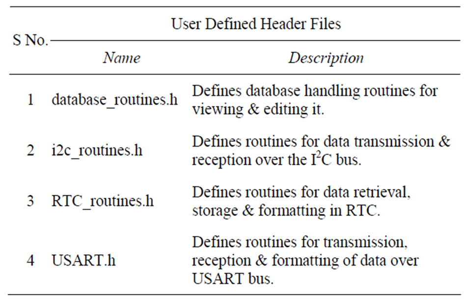
Table 1. Description of user defined header files.
gadget over the HyperTerminal window. Upon connecting the gadget to the PC through RS232 serial port and powering up the same via the USB port, we will be able to see the welcome screen shown in Figure 6, in the HyperTerminal window.
Upon pressing any key the user will get to see the main menu interface as shown in Figure 7 from which one can select the different options available.
Option 1 should be selected to set system time in the RTC chip. Time should be entered in 24 hour format along with the system date and day as shown in Figure 8. Upon filling all the details the chip gets automatically updated. After setting the system time the same could be viewed by selecting option 2 from the main menu interface upon which the details of the set system time, date and day appears as shown in Figure 9.
Option 3 from the main menu interface should be selected in order to edit the time-settings for the device under control. The example followed illustrates the procedure.

Figure 6. Welcome screen in HyperTerminal.

Figure 7. Main menu interface in HyperTerminal.
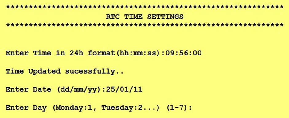
Figure 8. Editing RTC system time from HyperTerminal.

Figure 9. Viewing RTC system time from HyperTerminal.
Example: We need to edit the time-settings for the device under control in order to achieve a sequence of operation as given in the time chart shown in Figure 10.
In order to implement this sequence of operation for the device under control, we set the reference time, which in this case is conveniently chosen as 00:32 hrs.
We set the initial status of the device as OFF and also the four relative time-settings with reference to the reference time are entered. Hence we enter four datapoints in the menu and go on entering the data point details along with the device status for the set relative time. Upon entering the last data point the gadget will automatically save the database to its internal EEPROM. These sequences of operations are depicted in Figures 11-13.
In order to view the saved database in the EEPROM the user can select option 4 from the main menu interface. The gadget then reads the database from its EEPROM memory formats the data into user readable form and finally displays it in the HyperTerminal Window as shown in Figure 14.
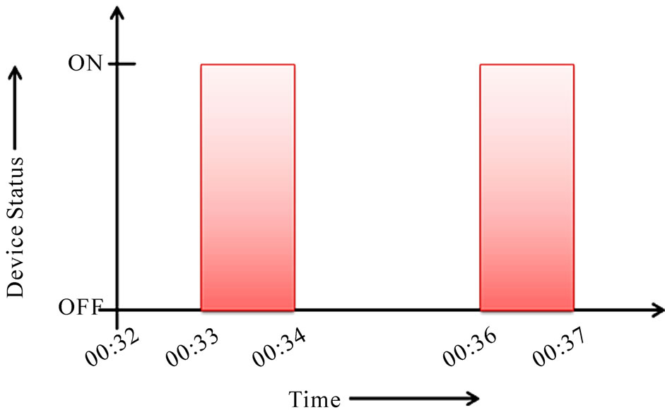
Figure 10. Time chart.

Figure 11. Editing time-settings database by entering the reference time.
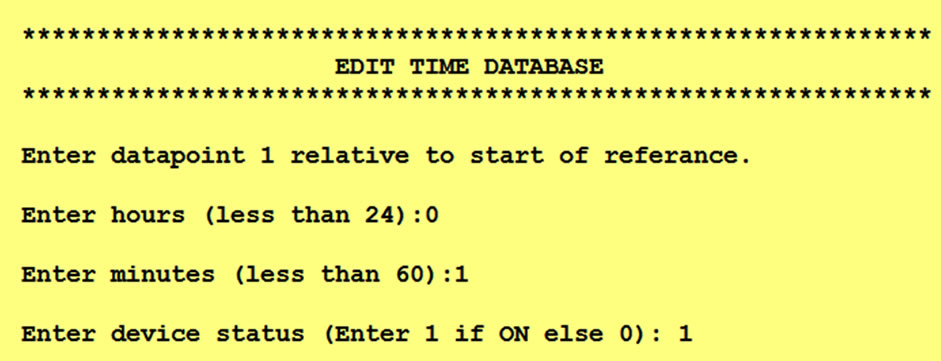
Figure 12. Entering the first relative datapoint details.
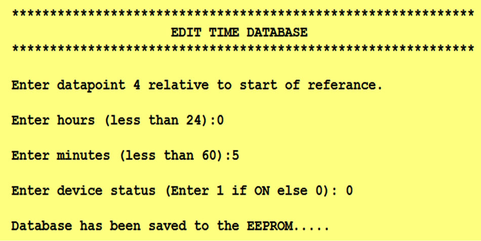
Figure 13. Entering the last relative datapoint details.
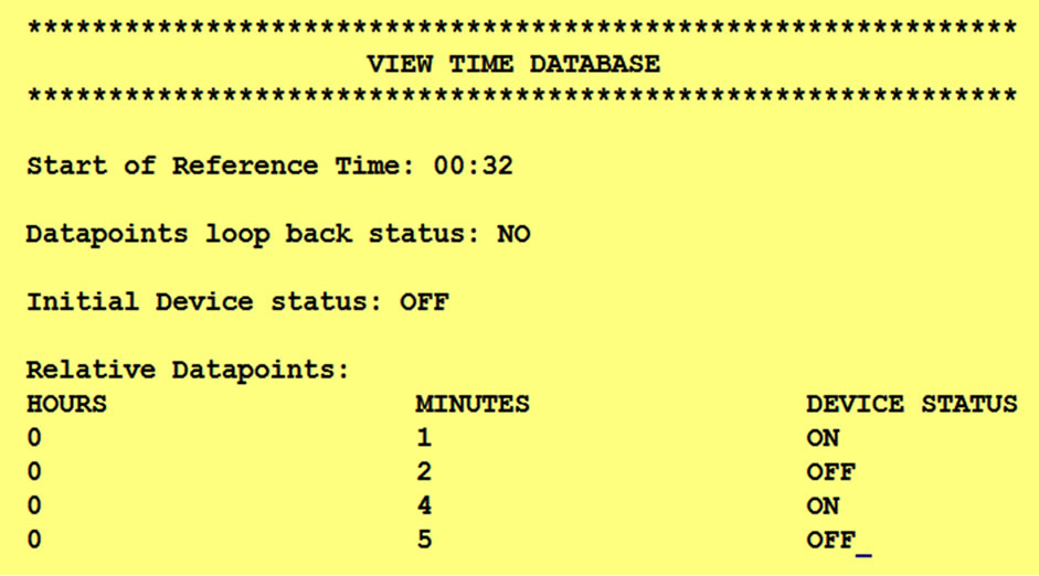
Figure 14. Viewing the database saved in the EEPROM through Hyperterminal.
Once the gadget is successfully configured with the system time and the required time-setting database for the device under control, the device should be detached from the PC. It should then be switched over to the standby mode by releasing switch S1. Lastly, connect it to the driver module via the USB port on the gadget
5. Conclusions
A timer cum time-keeper has been designed, fabricated and tested. Snapshots of the author’s prototype are shown in Figure 15-17. A complete single sided PCB layout for the gadget circuitry is shown in Figure 18. This timer module can be used for preset time alarms, to switch on or off domestic lights or other gadgets at any time of the day for security reasons or alarms. This can be built as a programmable PLC module with multiple outputs, which will facilitate its operation based on multiple inputs and timings, which can programmed externally.
The gadget could also be effectively used to time synchronise the sensor nodes in a Wireless Sensor Network deployed for Precision agriculture where each sensor nodes need to detect temperature, light levels and soil moistures intermittently and communicate their data over the wireless network. This intermittent operation of these sensors nodes call in for a low duty cycle operation wherein these sensor nodes would be put to sleep when not in use and would be woken up only at specific instants of time when data is required for analysis. In such a scenario sensor nodes need to sleep and wake together so that they can periodically communicate. Errors in the timing mechanism will create inefficiencies that result in increased duty cycles. The Real Time Keeper discussed here could then be used to put these sensor nodes in sleep or wake-up state according to the timing requirements configured. All the Real Time Keeper modules attached to the sensor nodes would then be configured remotely over a ZigBee/Bluetooth Wireless Link operating in the transparent mode. The configuration data for all the Real Time Keeper modules will be broadcasted over the wireless link so that all the sensor nodes attached to the time
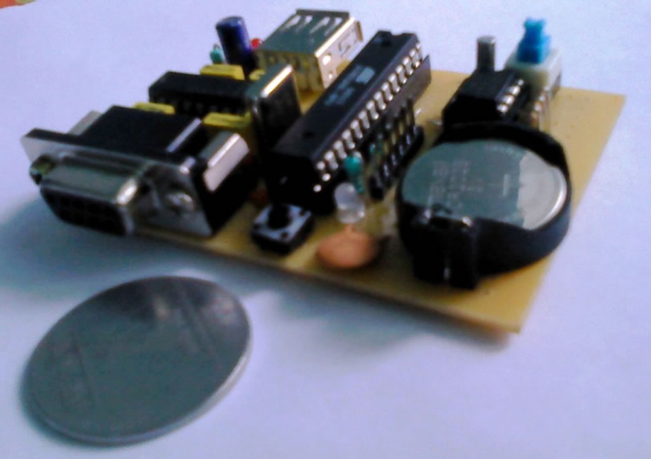
Figure 15. Author’s prototype of the gadget.
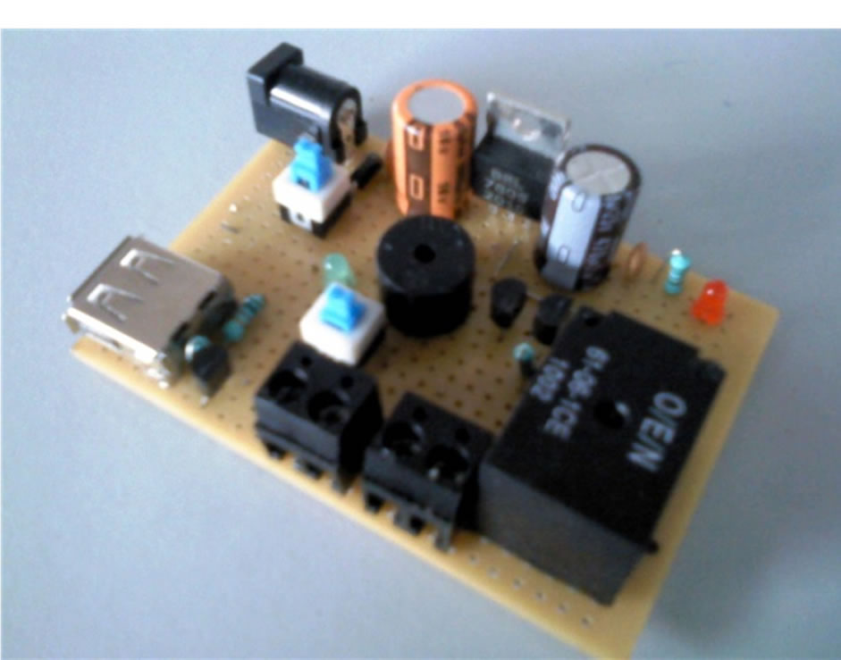
Figure 16. Author’s prototype of the driver module.
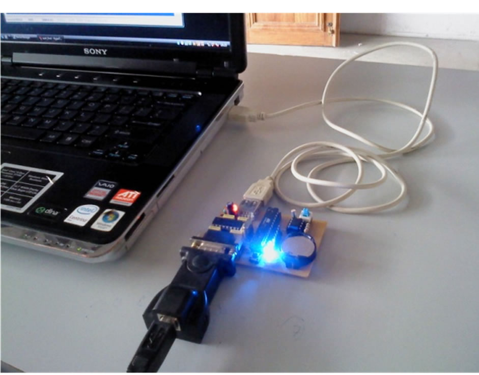
Figure 17. Author’s prototype when connected to PC for configuration.
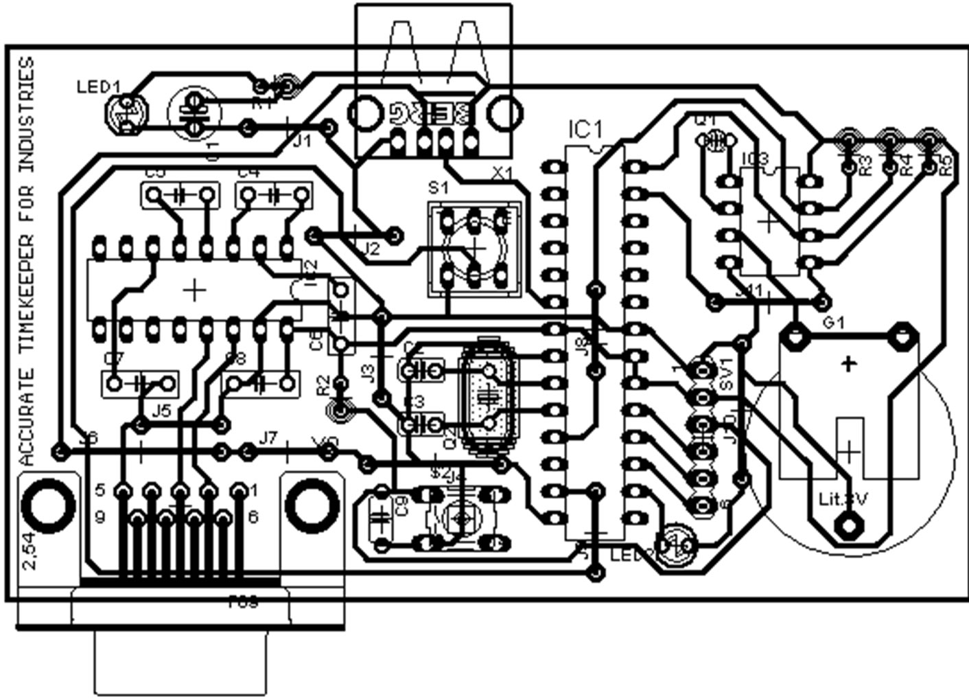
Figure 18. Single side PCB layout of the control circuit.
keeper module would be time synced.
REFERENCES
- “User Manual for Series 405 Timer with Instantaneous Relay,” Industrial Timer Company, Centerbrook.
- “User Manual for Series 407 Multi Mode Timer,” Industrial Timer Company, Centerbrook.
- “User Manual for Series RG21 Cycle Timer,” Industrial Timer Company, Centerbrook.
- “User Manual for Series GP2 Multifunction Timer,” Industrial Timer Company, Centerbrook.
- “DS1307 Datasheet,” Rev. 100208, Dallas Semiconductor, Maxim Integrated Products, Sunnyvale.
- “AVR Atmega 8 Datasheet,” Rev. 2486S-08/07, Atmel Corporation, San Jose.
- “AVR306: Using the AVR UART in C,” AVR Application Note, Rev. B-07/08.
- “Maxim MAX232 Datasheet,” Rev. 11-2/03, Maxim Integrated Products, Sunnyvale.
- “AVR315: Using the TWI Module as I2C Mmaster,” AVR Application Note, Rev. B-09/04.
- “AVR130: Setup and use the AVR Timers,” AVR Application Note, Rev. A-02/02.
- “LM7805 Datasheet,” Rev. 1.0.1, Fairchild Semiconductor Corporation, San Jose.
- “AVR100: Accessing the EEPROM,” AVR Application Note, Rev. C-09/05.
- “AN504: Design Consideration for Dallas Semiconductor Real-Time Clocks,” Maxim Application Note, Rev. A- 02/04.
- “BC548 Datasheet,” Rev. A2-August 2002, Fairchild Semiconductor Corporation, San Jose.
- F. Eady, “Networking and Internetworking with Microcontrollers,” 2nd Edition, Newnes Publications, 2004.
- J. J. Labrosse, “Embedded System Building Blocks, Complete and Ready-to-Use Modules in C,” 2nd Edition, Miller Freeman Publications, San Francisco, 2000.