Materials Sciences and Applications
Vol.3 No.8(2012), Article ID:21803,4 pages DOI:10.4236/msa.2012.38080
The High Energy Region of the Absorption Edge of a-Si:H, a Theoretical Study—III
![]()
Physics Department, College of Science for Women, Baghdad University, Baghdad, Iraq.
Email: *salwan_kamal@yahoo.com
Received May 4th, 2012; revised June 8th, 2012; accepted July 12th, 2012
Keywords: High energy; Absorption Edge
ABSTRACT
In this paper we try to give a reasonable account for the origin of the experimental optical energy gap Eo of a-Si:H deduced from the plot due to Cody ( vs. E). Using a realistic model density of states diagram for a-Si:H and the constant dipole matrix element assumption, and a reasonable definition of the real optical energy gap EG, a new theoretical equation for ε2(E) was derived. The plot of the square root of this function
  as a function of the photon energy E for appropriate fitting parameters gives a straight line fit in the energy region of significance extrapolating to the energy axis at a value similar to the experimental optical gap but about 0.1 eV lower than the theoretical optical gap EG proposed in our paper. We conclude that the experimental optical gap Eo does not necessarily coincide with any optical transition threshold in the density of states diagram of a-Si:H.
1. Introduction
In two previous papers [1,2], we concluded from the re-analysis of the experimental results of Jackson et al. [3] for the density of states convolution integral J(E) as a function of photon energy E for GD a-Si:H in the energy range (1.6 - 3.7 eV), that the theoretical model due to Cody [4] is the suitable theoretical model for the interpretation of the optical data at the high absorption region of the optical absorption edge of this important material.
This model assumes a parabolic density of states (DOS) distribution near each of the valence and conduction band edges (similar to the Tauc [5] model), and a constant dipole matrix element (Tauc assumed a constant momentum matrix element).
The problem of the interpretation of the optical energy gap Eopt is still a matter of controversy in literature [4,6]. For example in the case of our analysis, the optical gap obtained from the plot attributed to Cody ( vs. E) which is ~1.68 eV does not match with the value of the mobility gap of Jackson et al. [3] samples i.e. ~1.93 eV. While the gap obtained from the famous Tauc plot (
 vs. E) ~1.89 eV is significantly closer to the value of the mobility gap for Jackson et al. samples.
In this paper we try to give a reasonable explanation for this problem, which we hope that it gives a possible clue towards the understanding of the problem of the interpretation of the optical energy gap problem in amorphous semiconductors.
2. Theory
The imaginary part of the dielectric constant ε2(E) for amorphous semiconductors is given by [3]:
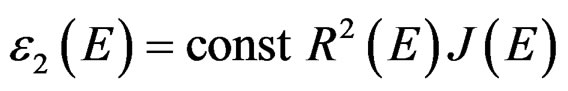 (1)
(1)
where R2(E) is the normalized average dipole matrix element and J(E) is defined as:
 (2)
(2)
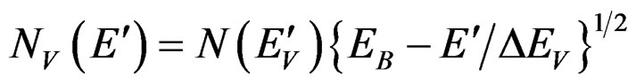
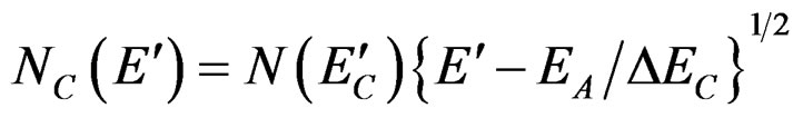
where Nv(E') and Nc(E') are the valence and conduction band density of states functions respectively and E' is the state energy.
It usually assumed that the density of states distribution near each of the valence and conduction band edges is some simple power law i.e. N(E')αE'm. If R2(E) also obeys a simple power law of the form R2(E)αE−q. The general solution of equation (1) using the above assumptions is [4]:
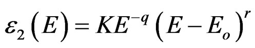 (3)
(3)
where K is a constant, r = 2m + 1 ( for symmetrical DOS), and Eo is a parameter usually identified with the optical energy gap Eopt (Eo = Eopt) though of course this is not necessarily true.
For the Tauc model [5]  and the momentum matrix element squared (P2(E)) is constant, thus q = 2 and r = 2 in equation (3), then the relation
 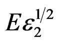 = A(E − Eo) gives a straight line with Eo as the Tauc gap.
For the Cody approach [4] the only variant with the Tauc approach is the assumption of a constant dipole matrix element R2(E) = const., Thus q = 0 and r = 2 in equation (3), then the relation  = B(E − Eo) gives a straight line with Eo different from the Tauc gap usually lower.
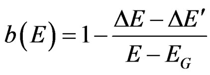
The optical energy gap Eo is obtained from the extrapolation of the straight line to the photon energy axis.
In this paper our main concern is with interpretation of Eo using a detailed model density of states for a-Si:H assuming a reasonable theoretical optical energy gap in order to deduce a new equation for ε2(E).
3. Our Theoretical Analysis
Figure 1 depicts the model density of states diagram based mainly on the standard model applied for electronic quality a-Si:H. Here we take every possible detail into account accept for the effect of exponential tails on the resulting Eo which was studied previously by Malik and O’Leary [7]. In this figure we note the following:
1) The density of states distribution in the extended states near each of the valence and conduction band edges Ev and Ec respectively is parabolic ( ).
).
2) In the localized states regions just under the conduction band edge (Ec −  =
= ), and just above the valence band edge (
 − Ev =
 ) the density of states distributions are also parabolic.
3) In the regions far away from each of the band edges, the density of states distributions is exponential in nature.
4) The energy interval (ΔE) in figure 1 is (Ec − EA = EB − Ev) i.e. the density of states diagram is assumed to be symmetric.
5) The energy interval (ΔE') in the same figure is ( − EA = EB −
 ).
).
6) The real optical energy gap which is defined as EG represents in this diagram the assumed threshold for optical transitions responsible for the high energy region of the absorption edge which is ( − Ev or Ec −
 ).
).
This last definition of EG is based on the experimental findings of Jackson et al. [3] that the matrix element is nearly the same for localized-extended and extendedextended transitions. We call EG the real optical gap because it is defined from the density of states diagram and not from the analysis of optical data i.e. Eopt, there is no a priori necessity or assuming them equal.
According to figure 1:
 (4a)
(4a)
 (4b)
(4b)
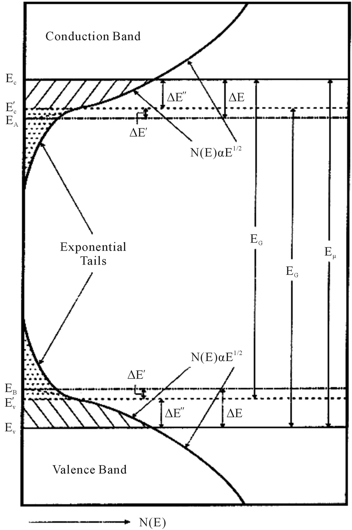
Figure 1. The model density of states diagram of a-Si:H.
where N( ) and N(
 ) are the densities of states at the valence and conduction band edges respectively.
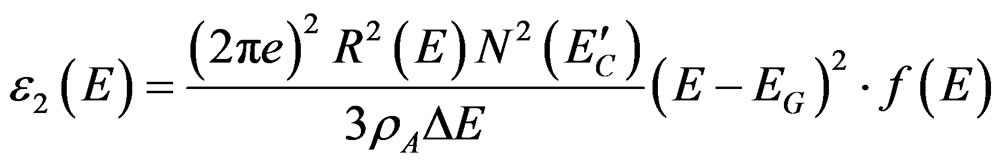
For amorphous silicon and un-polarized light the prefactor in equation (1) is equal to (2πe)2R2(E)/3ρA [3] where ρA is the atomic density, taking this into account we substitute equations (2) and (4) in equation (1) to get [6]:
 (5)
(5)
where:
 (6a)
(6a)
 (6b)
(6b)
 (6c)
(6c)
We see that equation (5) includes three main parameters of the model density of states of figure 1 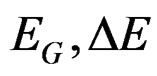 and
and 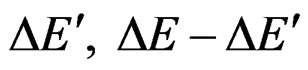 in equation (6b) is just
 .
.
For a-Si considering  is that for c-Si, equation (5) becomes:
 (7)
(7)
where R2(E) is in units of Å2, E in eV, and N(Ec) is in units of eV−1∙cm−3
4. Results and Discussion
The function f(E) is plotted for chosen parameters (X = EG) = 1.78 eV, (Y = ΔE) = 0.18 eV and (Z = ΔE') = 0.03 eV and the result is depicted in figure 2.
If we plot the square root of this function i.e.  as function of E, then figure 3 gives a straight line that fits the equation 0.654E−1.68, we see that the extrapolation to the x-axis is equal to ~1.68 eV which is equal to that for Jackson et al. [3] samples.
Thus although the assumed real optical gap EG in our model was 1.78 eV the optical gap that results from the 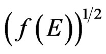 vs. E) plot is 1.68 eV which 0.1 eV smaller. Thus we conclude that the experimental optical energy gap Eopt is not an accurate marker of the energy gap responsible for the threshold of optical transitions responsible for the high energy region of the absorption edge.
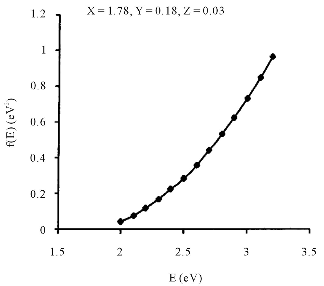
Figure 2. plot of the function f(E) vs. E for the fitting paramers X = EG = 1.78 eV, Y = ∆E = 0.18 eV, Z = ∆E' = 0.03 eV.

Figure 3. Plot of  vs. E for the fitting parameters X = 1.78 eV, Y = 0.18 eV, Z = 0.03 eV. It is fitted to the straight line equation 0.654(E−1.68).
Malik and O’Leary [7] also reached a similar conclusion albeit for a different reason which is the exponential band tailing at the valence and conduction band edges.
We may also conclude and suggest that may be by joining the two approaches i.e. accounting for exponential band tailing suggested by Malik and O’Leary [7] and our suggestion that the real optical gap does not necessarily start at the valence and conduction bands edges as suggested originally by Tauc (5) might be the right clue to account for the physical origin and the value of the experimental optical energy gap (Eopt) deduced from the plot due to Cody [4]  vs. E if it is adopted to analyze
  data of a-Si-H in the high energy region of the absorption edge.
REFERENCES
- S. K. J. Al-Ani, S. S. Al-Rawi and A. Ibrahim, “The High Region of the Absorption Edge of a-Si:H I, an Analytical Study,” World Renewable Energy Congress-IX Florence Italy, 2006.
- S. K. J. Al-Ani, A. Ibrahim and S. S. Al-Rawi, “The High Region of the Absorption Edge of a-Si:H II, Derivative Methods Analysis,” World Energy Congress-X and Exhibition (WRECX), 2008.
- W. B. Jackson, S. M. Kelso, C. C. Tsai, J. W. Allen and S.-J. Oh, “Energy Dependence of the Optical Matrix Element in Hydrogenated Amorphous and Crystalline Silicon,” Physical Review B, Vol. 31, No. 8, 1985, pp. 5187-5198. doi:10.1103/PhysRevB.31.5187
- G. D. Cody, “The Optical Absorption Edge of a-Si:H,” In: J. I. Pankove, ed., Semiconductors and Semimetals, Academic Press, Waltham, 1984, p. 11.
- J. Tauc, R. Grigorovici and A. Vancu, “Optical Properties and Electronic Structure of Amorphous Germanium,” Physica Status Solidi, Vol. 15, No. 2, 1966, pp. 627-637. doi:10.1002/pssb.19660150224
- A. Ibrahim, “A Theortical Study of the High Absorption Region of the Optical Absorption Edge of Hydrogenated Amorphous Silicon (in Arabic),” Ph.D. Thesis, Baghdad University, Baghdad, 2002.
- S. M. Malik and K. O’Leary, “Deviations from SquareRoot Distributions of Electronic States in Hydrogenated Amorphous Silicon and Their Impact upon the Resultant Optical Properties,” Journal of Non-Crystalline Solids, Vol. 336, No. 1, 2004, pp. 64-70. doi:10.1016/j.jnoncrysol.2003.12.042
NOTES
*Corresponding author.
#Present address: NCPW, P.O. Box (25777), Doha, Qatar.