Journal of Modern Physics
Vol.4 No.2(2013), Article ID:27897,11 pages DOI:10.4236/jmp.2013.42030
Dust Plasma Effect on the Etching Process of Si[100] by Ultra Low Frequency RF Plasma
1Engineering Science Department, Faculty of Community, Umm Al-Qura University, Mecca, Saudi Arabia
2Department of Physics, Faculty of Science, Beni-Suef University, Beni-Suef City, Egypt
3Physics Department, Faculty of Science, Al-Azhar University, Cairo, Egypt
Email: ahmed_galaly@ yahoo.com
Received November 25, 2012; revised December 27, 2012; accepted January 7, 2013
Keywords: Dust Plasma; Ultra Low Frequency; Ion Etching; Ion Chemical Etching; Volumetric Rate of Loss
ABSTRACT
Dust-plasma interactions play vital roles in numerous observed phenomena in the space environment, their scope in the industrial laboratory has grown rapidly in recent times to include such diverse areas as materials processing, microelectronics, lighting and nuclear fusion. The etching processes of Si wafer has been studied using Ultra low frequency RF plasma (ULFP) at (1 KHz) by two different techniques namely: ion etching using inert gas only (e.g., argon gas), and ion chemical etching using an active gas (beside the inert gas) such as oxygen. In the case of large dust particle, the dust might act as a floating body in the plasma collecting equal fluxes of electrons and ions. The velocity of the ions flux out from the mesh (cathode) and cause ion sputtering for the sample (Si-Wafer) measured, moreover the rate coefficient for collection of electrons and ions by dust (K) is calculated here, the presence of dust, however, may itself cause loss process. As the plasma density increases, the etching rate increases and the volumetric rate of loss of electron and ions due to dust particle increases (K). A comparison between the volumetric rate of loss (K) due to ion chemical etching (75% Ar/25% O2) and ion etching (Pure Ar) has been carried out.
1. Introduction
Plasma processing is one of the key technologies in the fabrication of modern silicon devices. It is applied to approximately one third of the several hundred fabrication steps. Plasma etching enables together with advanced lithography the high volume production of submicron structures. The significant deference to the formerly used wet etching in liquid chemicals is its ability to keep the mask dimensions much more accurately [1]. One of the most useful properties of a glow discharge is that it can modify the physical, chemical, and electrical properties of a material surface. The modification of the material surface changes the interface properties between the surface and the film deposited after plasma pretreatment [2].
While different etching processes are selected depending upon the particular material to be removed. Wet chemical processes result in isotropic etching where both the vertical and lateral etch rates are comparable, whereas dry etching processes like sputter etching, plasma etching, ion beam etching, and reactive ion etching are anisotropic. Among the dry etching techniques, plasma and reactive ion etching are the most popular in semiconductor processing [3].
Dry Plasma etching method [included ion etching using inert gas only (e.g., argon gas), and ion chemical etching using an active gas (beside the inert gas) such as oxygen] involves the use of two RF sources: Inductively coupled plasma (ICP) and Capacitive coupled plasma (CCP) sources, widely, in the literature for dry etching of different materials [4].
ICP has attracted interest due to its simple structure and the absence of a magnetic field. A few researchers have carried out SiO2 etching in ICP. However most of them have reported that using ICP for etching introduces some problems, such as low etching selectivity, local side etching and charge build up damage. Plasma parameter variation as a function of a mixing ratio in an electron temperature control system using a grid are investigated [5]. Under the grid, the electron temperature, as well as electron density, is a strong function of a mixing ratio. The electron temperature decreases with a mixing ratio of a molecular gases (O2), and the large inelastic cross section of molecular gas is the reason for the decrease in the electron temperature.
Capactively coupled plasma (CCP) has been widely used for silicon dioxide (SiO2) etching. But for high anisotropic and fast etch, other sources which have high density under low pressure are necessary. There has been much research on high density sources such as electron cyclotron resonance, helicon [6] and inductively coupled plasma (ICP) [7]. Inductively coupled plasma (ICP) device contains a mesh grid to control the electron temperature and density [8].
Some authors suggested that water vapor inductively coupled plasma can be used as a useful dry etching plasma reactors [9,10]. A comprehensive simulation study of the time analysis of the profile charging during the etching processes of SiO2 in plasma also was carried out [11]. Capacitive coupled plasma (CCP) were used [12-16] an ion etching CCP system operated by 13.56 MHz to study the fabrication of the silicon nanostructures using local gallium implantation. This ion reactive system is useful tool for nanotechnology applications. Rate of etching was also investigated [17].
2. Experimental Setup
In the present experiment two kinds of dry etching (mainly a physical etching, e.g. sputtering), ion etching and ion chemical etching were used. In the simplest case, chemically active oxygen is added to the inert gas (argon) to change the etching rate and provide a high selectivity of the etching. Moreover in the ion chemical etching, there are two sources of the reactions: surface reaction and plasma reactions.
The CCP plasma system consists of a stainless steel chamber has few glass ports, connected to vacuum system and evacuated to 10−4 torr. The used gases were then admitted to the system via needle valves. The RF plasma source has two parallel circular electrodes; a copper anode plate of 4.5 cm diameter and an aluminum mesh grid (30 lines per inch) working as a cathode, and placed above the anode at a gap distance of 3 - 5 mm. An Si[100] wafer was fixed above the mesh grid whereas the produced plasma collides with the sample surface and ion etching takes place. A PTFE insulated material was placed around the electrodes in order to confine the plasma in the area of the Si-wafer and prevents the build up of charged sheaths on the electrodes surface and henceforward enhanced the plasma density up to the required values for etching. Figure 1 shows the schematics diagram of the plasma cell. An RF capacitive coupled plasma was generated using ultra low frequency (ULF) power supply of one KHz frequency, few hundreds Volts and 50 - 100 mA currents. A schematic diagram of the RF electric circuit is shown in Figure 2.
The characteristics of the dust and holes of the Si-wafer after treatment by plasma were investigated using Jeol Scanning Microscope (JSM) and Optical Scanning Microscope. The characteristics of the formed plasma (electron temperature, density, energy distribution function. etc.) were measured at different discharge conditions (e.g. gas pressure, gases percentage, electric powers…). Langmuir double probe and faraday cup probe were fixed in the emerged plasma [18-22].
The Faraday Cup probe was used to measure the velocity distribution function of the plasma observed over the mesh (intense glow cylinder zone over the mesh) where the Faraday Cup probe faced the mesh at a distance equal to 4.5 cm from the mesh and 4.3 cm from the anode, at their axial axis. The Faraday Cup probe consists of a cup of brass of diameter 1.5 cm and depth 1 cm as shown in Figures 3(a) and (b), it was connected to the negative terminal of a DC power supply. The circuit consists of a DC power supply adjusted to 60v across a resistance of value 110 Ω, 10 turns potentiometer (50 KΩ) to vary the probe bias from +100 to −100 volts but in our case we determined the negativity of the Faraday Cup as shown in Figure 4(a). Moreover, the brass cup was covered by an earthed closed cylindrical cup with a hole at it’s center, with diameter D = 2 mm) to avoid the noise and to make a filtration. The negativity of the faraday cup attracts the positive ions emitted from the mesh and repel the electrons.
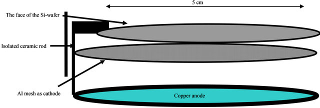
Figure 1. A Schematic diagram of the plasma etching cell.
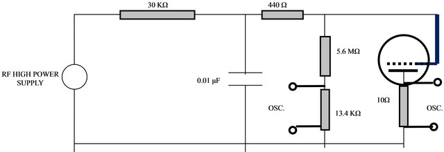
Figure 2. The RF electrical discharge circuit.
 (a)
(a)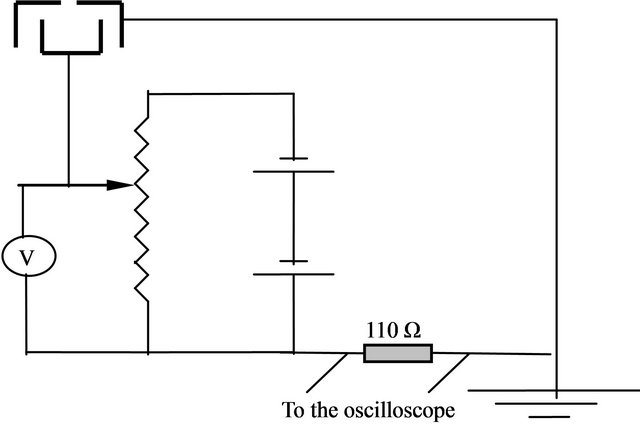 (b)
(b)
Figure 3. (a) The shape of the faraday cup probe; (b) The faraday cup probe circuit.
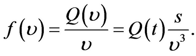
The velocity of ions and plasma density may be calculated from the Faraday Cup probe, where the ion velocity distribution function given by:
 (1)
(1)
where (S) the distance between the Faraday Cup and the cathode (mesh),  the velocity of the ions emerging from the mesh,
  the Faraday Cup current, and
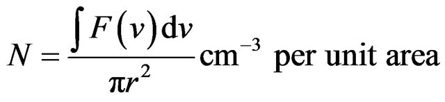
  the ion velocity distribution function. Where we can get the density per unit area by integrating the ion

Figure 4. The temporally variation of ion current distribution in pure argon gas at 1 mbar pressure and at different applied voltage.
velocity distribution [23]:
 (2)
(2)
where r is the radius of the hole at the center of the faraday cup.
The etching processes of Si(100) wafer has been studied using two different techniques namely: ion etching using inert gas only (e.g. argon gas) and ion chemical etching using an active gas (beside the inert gas) such as oxygen. In the present work a silicon wafer was used with the following properties: Single Crystalline, Si[100], n-type, resistively 1 - 10 Ω∙cm, thickness 300 μm, and the diameter 5 cm.
3. Experimental Results and Discussion
Ions are accelerated onto the substrate at high kinetic energy. When the ions strike the surface atoms, momentum transfer takes places, and the atoms are knocked out of the surface and into the gas phase, where they are pumped away. Taking into consideration that the sputtered atoms (from Al mesh, substrate of the Si wafer, and the polymer of any organic material from the substrate of the wafer) can be recondensed onto a nearby region (substrate) to form a coating, thus sputtering can be used to both etch and deposit [24-26] or an important case for dust plasma effect on the nano-etching process of Si.
The velocity of the ions flux out from the mesh (cathode) and cause ion sputtering for the sample (Si-Wafer) over the mesh, measured by Faraday Cup probe method to give information averaged over a large volume of plasma. Moreover other parameters such as ion temperature, ion energy distribution and ion kinetic energies were measured to understand the atomic processes which occur in the discharges, e.g., the influence of ions on the etching of semiconductor materials in plasma reactors.
An important character of the glow discharge is the velocity of the ions flux and the density of ions moving out of the mesh (cathode) which cause the ion sputtering of the present sample (Si-Wafer). Faraday Cup probe method has one advantage over all other diagnostic techniques since it produced local measurements. Almost all other techniques, such as spectroscopy, give information averaged over a large volume of plasma.
Figure 4 shows the temporally variation of ion current distribution curves (ion current of the Faraday Cup) I(t) at 1 mbar in the range of 0 - 100 μsec and at different applied voltage in pure Ar discharge. It is noted that, a large values of applied voltage are used to sure that the ion current enter through the Faraday Cup hole, whenever the applied voltage is increased, the ion current is increased and the bandwidth of the signal is increased, moreover the maxima values of the ion current signal is increased. In the case of the mixture of  discharge, similar curves were obtained as shown in Figures 5(a)-(e).
The ion velocity distribution was computed using the temporally variation of ion current distribution curves and Equation (1), where Figures 6 and 7(a)-(e) at the same pressure (1 mbar) show the velocity distribution at different applied voltage. The velocity was in the range of 105 cm/sec, and as the ion velocity was increased, the area under the curves was increased, and the maximum value of the ion velocity distribution function signal was increased.
Figures show that when the applied potential increased, the peak (maxima) of the curves shifted from (maximum velocity and minimum ion velocity distribution function) value to (minimum velocity and maximum ion velocity distribution function) value. Moreover (IVDF) is assumed to be accelerated (drifting) Maxwellian distribution.
The ion density per unit area was computed by integrated the area under the curves of the ion velocity distribution, shown in Figures (using Equation (2)).
It is concluded that as the applied voltage increased, the density per unit area increased. And as the pressure increased the ion density per unit area increased.
It is concluded that as the applied voltage increased, the density per unit area increased, the ion density Ni per unit area in the case of the mixture of (25% O2/75% Ar) discharge is in the range of 108 cm−3, where Ni for pure Ar in the range 109 cm−3, i.e. Ni decreased by adding a molecular gas such as (O2) to argon, may be attributed to oxygen molecules entering the discharge suffer inelastic collisions with energetic electrons, leading to dissociation, excitation and ionization. Moreover a part of the energy go to the excitation process of the O2 molecules, and the other part go to the dissociation process so no sufficient energy to ionization process [27,28].
The fresh Si-wafer was placed in the abnormal glow region of the RF plasma system for times ranging from 25 - 75 min at a pressure of 1 torr and at constant base voltage of 700 volts. It was noticed that by increasing the etching time the holes of the etched surface became wider and then contact together to form more wider holes after 30 min. The similarity in the surface morphologies from 30 - 75 min implies that the etched surface processes is a self-similar structure in time scale.
For pure argon, the electrons may have a Maxwellian energy distribution function whereas the electrons temperatures are between (5.75 - 4.05 eV) at the center of the mesh and (6.74 - 3.34 eV) at the edge of the mesh. For argon-oxygen mixture (75% Ar + 25% O2) the temperature was (4.018 - 2.835 eV) at the center of the mesh. The electron density for pure argon was (4.2 × 10¹⁰ to 20 × 1010 cm−3) at the center of the mesh and (1.57 × 10¹⁰ to 13.7 × 1010 cm−3) at the mesh edge. For argon-oxygen mixture the density was (5.7 × 1010 cm−3 to 20.6 × 1010 cm−3) at the center of the mesh in a pressure range of (0.5 - 5 torr).
Two different explanation to this plasma etching processes may be take place:
First step; the surface was bombarded by both electrons and positive ions of the formed plasma, it may initially collects much more electron current due to the higher mobility of the lighter electrons. As a result, the wafer becomes negatively charged relative to the plasma bulk. At some negative potential, the electron and ion fluxes will become equal since more electrons are repelled from the object and positive ions are accelerated toward it.
Second step: based on the following sequence of microscopic reaction steps. Electrons are accelerated by RF electric field and inelastic collisions occur with suitable precursor molecules to produce ions, atoms, and free
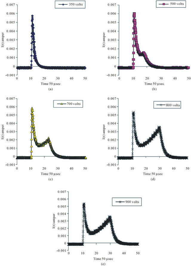
Figure 5. The temporally variation of ion current distribution at 1 mbar for the mixture of (O2/Ar) discharge at different applied voltage (350, 500, 700, 800, 900 volts).
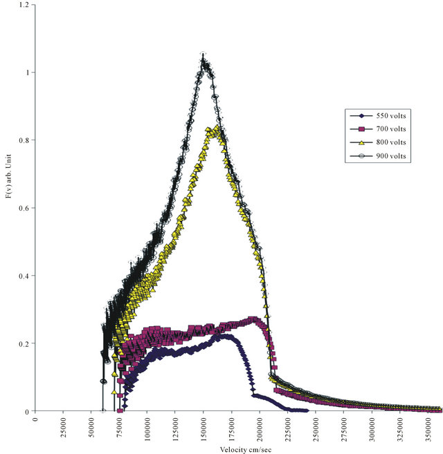
Figure 6. The ion velocity distribution function F(v) at 1 mbar and different applied voltage of Argon.
radicals. A complex mixture of reactive species is produced. Neutral and ionic reactive species strike the surfaces that are in contact with them to form products that are volatile.
The electron temperature is a strong function of a mixing ratio, the decrement in the electron temperature with a mixing ratio is mainly due to the large inelastic cross section of the mixed gases, the increasing in the sheath length around the grid (mesh) wires and the dissociation of the molecular oxygen gas (O2) by argon atoms beside the ionization.
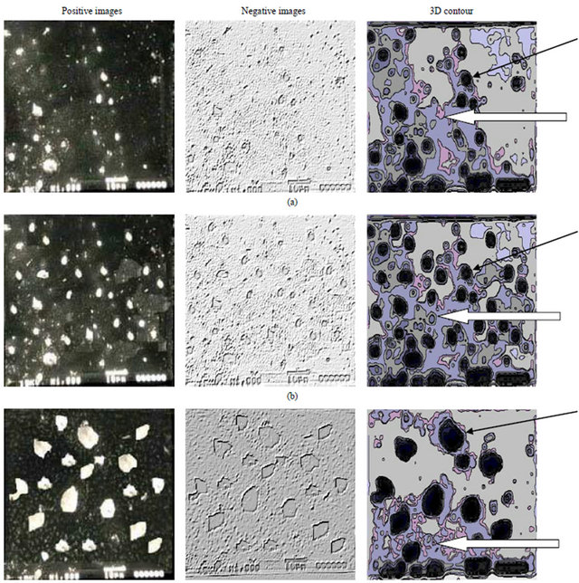
The etched surfaces of the Si wafer was investigated using Optical Scanning microscope and Joel Scanning Microscope) as shown specially in Figure 8 for pure Ar. The characteristics of the etched sample were measured using the images of the scanning microscope.
The values of Hole width (ω), Hole Depth (h) holes, Average distance between holes and Etching Rate (Ret) were changed due to the contamination by particulate (dust) effect which resulting from polymerization due to silicon etching are more for pure Ar than (75% Ar/25% O2) in the RF Glow discharges, where the particulates
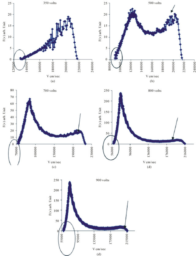
Figure 7. The ion velocity distribution function F(v) and the velocity of ions V at 1 mbar for the mixture of (O2/Ar) discharge at different applied voltage (350, 500, 700, 800, 900 volts).
Positive images Negative images 3D contour
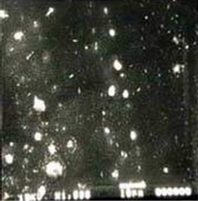
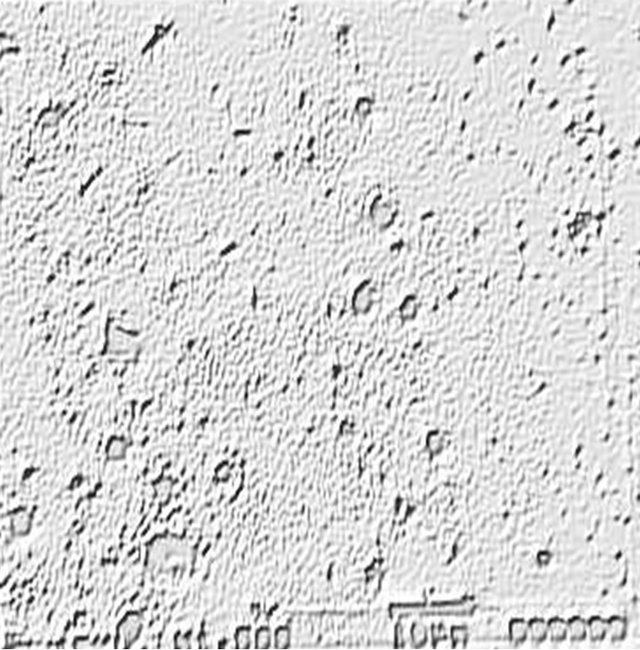
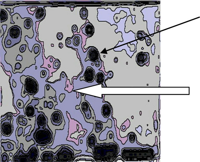
Figure 8. Are the Jeol scanning microscope images of ion etching by 100% Ar, plasma etched Si(100) substrates for t = 30, 45 and 75 min, where the white arrow show the dust regions and the black arrow show the etched area. (a) t = 30 min; (b) t = 45 min; (c) t = 75 min.
have the following characteristic:
1) particulates are sufficiently large, they will negatively charge and act as Coulomb-like scattering centers for electrons. Where if a dust particle is large enough for a sheath to form at its surface as shown by the white arrows in Figure 8 especially for pure argon, then the dust acts as a floating body in the plasma collecting equal fluxes of electrons and ions. The volumetric rate coefficient for collection of electrons and ions by dust (K) [29, 30] is:
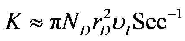 (3)
(3)
 , ND, rD are the ion velocity, the dust density and the particulate radius, respectively.
2) The volumetric rate of loss of electrons and ions (K) at applied voltage 700 volts and P = 1 mbar can be computed as shown in Figures 9 and 10 using Equation (3), under specific condition by Kushner model (103 < ND < 106
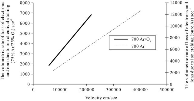
Figure 9. The volumetric rate of loss of electrons and ions due to ion chemical etching and ion etching at applied voltage 700 volts and P = 1 mbar for (ND = 103, rD = 1 μm).
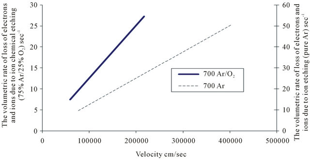
Figure 10. The volumetric rate of loss of electrons and ions due to ion chemical etching and ion etching at applied voltage 700 volts and P = 1 mbar for (ND = 103, rD = 2 μm).
cm−3, 0.1 < rD < 2 μm and the velocities in the range of 105 cm/sec), taking the velocities values from Figure 6 for pure Ar and from Figure 7 for (75% Ar/25% O2) mixture.
3) a comparison between the volumetric rate of loss (K) due to ion chemical etching and ion etching has been carried out as shown in Figures 9 and 10 for (ND = 106, rD = 1 μm, 2 μm). As the ion velocity was increased, the values of (K) due to ion etching by pure Ar was more than those due to ion chemical etching by (75% Ar/25% O2) mixture, the values of (K) in the range of 104 Sec−1.
4) To demonstrate the perturbation in the densities of electrons and excited states which could occur as a result of the collection of electrons and ions by dust, we included that:
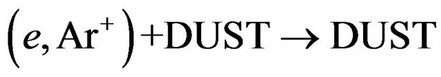
i.e., the presence of dust, however, may itself be a loss process [31].
4. Conclusion
Finally as the plasma density increases, the etching rate increases and the volumetric rate of loss of electron and ions due to dust particles increases also. Moreover the ion chemical etching elongate the etching time more than the ion etching without changing the etching process to deposition process. For Ar+ ion energy, only 5% of it is usually spent for sputtering, the other 95% being spent for heating the target material, damage and destruction the surface, ion incorporation, secondary electron emission and electromagnetic radiation. So this process has low efficiency than ion chemical etching.
A small amount of oxygen (25% O2) added to an argon rf discharge (75% Ar) for ion chemical etching has been sufficiently to decrease the polymerization and increase the time of etching. Finally we can concluded that the presence of dust cause loss and delay in any process.
REFERENCES
- J. Hopwood, C. R. Guarnieri, S. J. Whitehair and J. J. Cuomo, “Langmuir Probe Measurements of a Radio Frequency Induction Plasma,” Journal of Vacuum Science & Technology A: Vacuum, Surfaces, and Films, Vol. 11, No. 1, 1993, p. 152.
- A. R. Galaly, “Nano-Coating Process for Si[100] Wafer Using Atmospheric Pressure Plasma Jet (APPJ),” Journal of Modern Physics, Vol. 3, 2012, pp. 1031-1039. doi:10.4236/jmp.2012.39136
- H.-U. Kim, C. Yi and S.-W. Rhee, “The Effect of He or Ar/O2 Plasma Treatment on Si Surface Prior to Chemical Vapor Deposition of SiO2,” Journal of Materials Science: Materials in Electronics, Vol. 15, No. 1, 2004, pp. 37-41. doi:10.1023/A:1026240904706
- A. R. Galaly, M. A. Hassouba and U. M. Rashed, “Analysis of Cylindrical Langmuir Probe Using Experiment and Different Theories,” Plasma Physics Report Journal, Vol. 39, No. 3, 2013, pp. 1-8.
- A. R. Galaly and F. F. El Akshar, “Comparison between Experimental and Theoretical Consideration for Three Different Schematics Plasma Reactors,” 8th International Scientific Conference Environment, Development, and Bioinformatics, Cairo, 26-28 March 2012.
- N. Hershkowitz and R. A. Breun, “Diagnostics for Plasma Processing (Etching Plasmas),” Review of Scientific Instruments, Vol. 68, No. 1, 1997, p. 880. doi:10.1063/1.1147752
- K. H. Bai, J. I. Hong, S. J. You, C. K. Choi and H. Y. Chang, “The Effects of Mixing Molecular Gases on Plasma Parameters in a System with a Grid-Controlled Electron Temperature,” Physics of Plasmas, Vol. 9, No. 3, 2002, p. 1025. doi:10.1063/1.1436129
- A. Martsutani, H. Ohtsuski and F. Koyama, “Inductively Coupled Plasma Etching of Silicon Using Solid Iodine as an Etching Gas Source,” Japanese Journal of Applied Physics, Vol. 50, No. 3, 2011, 4 p. doi:10.1143/JJAP.50.06GG07
- Y. Takao, K. Eriguchi and K. Ono, “Effect of Capacitive Coupling in a Miniature Inductively Coupled Plasma Source,” Journal of Applied Physics, Vol. 112, No. 9, 2012, Article ID: 093306. doi:10.1063/1.4764333
- B. Radjenovic and M. Radmilovic, “3D Etching Profile Evolution Simulations: Time Dependence Analysis of the Profile Charging during SiO2 Etching in Plasma,” Journal of Physics: Conference Series, Vol. 86, No. 1, 2007, Article ID: 012017. doi:10.1088/1742-6596/86/1/012017
- M. A. Lieberman and C. Suwon, “Local and Global Particle and Power Balance in Large Area Capacitive Discharges,” Plasma Sources Science and Technology, Vol. 12, No. 2, 2003, p. 244. doi:10.1088/0963-0252/12/2/316
- N. Y. Babaeva and M. J. Kushner, “Penetration of Plasma into the Wafer-Focus Ring Gap in Capacitively Coupled Plasmas,” Journal of Applied Physics, Vol. 101, No. 11, 2007, 11 p. doi:10.1063/1.2736333
- D. Gahan, S. Daniels, C. Hayden, P. Scullin, D. O’Sullivan, Y. T. Pei and M. B. Hopkins, “Ion Energy Distribution Measurements in rf and Pulsed dc Plasma Discharges,” Plasma Sources Science and Technology, Vol. 21, No. 2, 2012, Article ID: 024004. doi:10.1088/0963-0252/21/2/024004
- K. Maeshige, G. Washio, T. Yagisawa and T. Makabe, “Functional Design of a Pulsed Two-Frequency Capacitively Coupled Plasma in CF4/Ar for SiO2 Etching,” Journal of Applied Physics, Vol. 91, No. 12, 2002, 8 p. doi:10.1063/1.1478138
- S. M. Han and E. S. Aydil, “Study of Surface Reactions during Plasma Enhanced Chemical Vapor Deposition of SiO2 from SiH4, O2, and Ar plasma,” Journal of Vacuum Science & Technology A, Vol. 14, No. 4, 1996, 9 p. doi.:10.1116/1.580082
- F. Ren, S. J. Pearton, J. R. Lothian, C. R. Abernathy and W. S. Hobson, “Reduction of Sidewall Roughness during Dry Etching of SiO2,” Journal of Vacuum Science & Technology B, Vol. 10, No. 6, 1992, 5 p. doi:10.1116/1.586075
- N. Bibinov, H. Halfmann and P. Awakowicz, “Determination of the Electron Energy Distribution Function via Optical Emission Spectroscopy and a Langmuir Probe,” Plasma Sources Science and Technology, Vol. 17, No. 3, 2008, Article ID: 035004. doi:10.1088/0963-0252/17/3/035004
- B. Doggett and J. G. Lunney, “Langmuir Probe Characterization of Laser Ablation Plasmas,” Journal of Applied Physics, Vol. 105, No. 3, 2009, Article ID: 033306. doi:10.1063/1.3056131
- G. Guethlein, T. Houck, J. McCarrick and S. Sampayan, “Faraday Cup Measurements of Ions Backstreaming into a Electron Beam Impinging on a Plasma Plume,” Proceedings of Linear Accelerator Conference, Monterey, 21- 25 August 2000, pp. 467-469.
- S. Cho and M. A. Lieberman, “Local and Global Particle and Power Balance in Large Area Capacitive Discharges,” Plasma Sources Science and Technology, Vol. 12, No. 2, 2003, p. 224. doi:10.1088/0963-0252/12/2/316
- A. R. Galaly and F. F. El Akshar, “Characterstics of Ultra Low Frequancy Plasma (ULFP) Producing Cathode Etching Process,” International Journal of Multidisciplinary Research and Advances in Engineering (IJMRAE), Vol. 5, No. I, 2013, pp. 169-179.
- A. R. Galaly and F. F. El Akshar, “A Comparison between Three Different Electrode Configurations in an Argon RF Plasma,” International Journal of Engineering Research and Industrial Applications (IJERIA), Vol. 6, No. 1, 2013.
- R. J. Shul and S. J. Pearton, “Handbook of Advanced Plasma Processing Techniques,” Springer-Verlag, New York, Inc., 2000.
- V. E. Fortov, A. G. Khrapak, S. A. Khrapak and O. F. Petrov, “Dusty Plasmas,” Physics Uspekhi, Vol. 47, No. 5, 2004, p. 447. doi:10.1070/PU2004v047n05ABEH001689
- A. A. Mamun and P. K. Shukla, “Charging of Dust Grains in a Plasma with Negative Ions,” Physics of Plasmas, Vol. 10, No. 5, 2003, pp. 1518-1520.
- C. Zafiu, A. Melzer and A. Piel, “Measurement of the Ion Drag Force on Falling Dust Particles and Its Relation to the Void Formation in Complex (Dusty) Plasmas,” Physics of Plasmas, Vol. 10, No. 5, 2003, 5 p. doi:10.1063/1.1569486
- M. J. McCaughey and M. J. Kushner, “A Model for Particulate Contaminated Glow Discharges,” Journal of Applied Physics, Vol. 69, No. 10, 1991, 10 p.
- K. Ostrikov, I. B. Denysenko, S. V. Vladimirov, S. Xu, H. Sugai and M. Y. Yu, “Low-Pressure Diffusion Equilibrium of Electronegative Complex Plasmas,” Physical Review E, Vol. 67, No. 5, 2003, 13 p. doi:10.1103/PhysRevE.67.056408
- M. Lampe, G. Joyce, G. Ganguli and V. Gavrishchaka, “Interactions between Dust Grains in a Dusty Plasma,” Physics of Plasmas, Vol. 7, No. 10, 2000, 11 p. doi:10.1063/1.1288910
- A. Garscadden, B. N. Ganguly, P. D. Haaland and J. Williams, “Overview of Growth and Behaviour of Clusters and Particles in Plasmas,” Plasma Sources Science and Technology, Vol. 3, No. 3, 1994, p. 239. doi:10.1088/0963-0252/3/3/001
- V. E. Fortov, A. V. Ivlev, S. A. Khrapak, A. G. Khrapak and G. E. Morfill, “Complex (Dusty) Plasmas: Current Status, Open Issues, Perspectives,” Physics Reports, Vol. 421, No. 1-2, 2005, pp. 1-103. doi:10.1016/j.physrep.2005.08.007