Journal of Modern Physics
Vol.2 No.12(2011), Article ID:16503,8 pages DOI:10.4236/jmp.2011.212185
Direct Optical Energy Gap in Amorphous Silicon Quantum Dots
Theoretical Nanoscience for Optoelectronic Devices Group, Department of Physics, College of Education (Ibn Al-Haitham), University of Baghdad, Baghdad, Iraq
E-mail: moafak@uobaghdad.edu.iq
Received September 21, 2011; revised October 29, 2011; accepted November 13, 2011
Keywords: Nanoscience, Confinements, Quantum Dot, Photoluminescence
ABSTRACT
A theoretical investigation of photoluminescence spectra for amorphous silicon quantum-dots (1 - 4 nm), at room temperature, were used to study the effect of both spatial and quantum confinements spontaneously via determination the energy peak of maximum intensity transition. The results show a continuous shifting toward low energy peak (red shift) and toward high-energy peak (blue shift), with the decreasing of quantum dot size, due to spatial and quantum confinements respectively. These results have leaded us to believe that such quantum dot size (1 nm) changes the nature of amorphous silicon optical band gap from indirect to direct transition material.
1. Introduction
Silicon is a dominant material in micro and nanoelectronics technology, but because of its indirect band structure, it has not been possible to use silicon as optoelectronics devices such as light emitting diode [1-3]. The recent advancement in silicon technology has led to the fabrication of zero-dimensional structure, which is called silicon nanocrystals or silicon nanoparticle [4]. The exceedingly small region of space it is suggested to be a name “dot”. Therefore; these structures can be called silicon quantum dots, SiQDs systems [5,6]. In fact, these dots are often described as artificial atoms [7,8] to reflect the importance of quantization phenomena on their properties [9]. The realization of a SiQDs system has opened amazingly new area of physical research and technology that deal with atomic scales. Since the active SiQDs have dimensions that are below ten nanometers, the properties of this material completely change for this range of size. Thus, SiQDs systems are considered as potential blocks for future nanoelectronics and nanophotonics [10]. But, in the process of searching for more efficient materials of lower dimension, it has been found that the amorphous silicon quantum dots, a-SiQDs, may be a convenient material for this purpose [11,12]. In fact, this retains to the bulk amorphous silicon two important advantages compared with crystalline silicon [13,14]: firstly, the luminescence efficiency in a-Si is higher than in c-Si, due to its structural disorder. Secondly, the bandgap energy of a-Si (1.6 eV) is larger than that of c-Si (1.1 eV). Therefore, a-Si is believed to be a good candidate for short wavelength light emitters [13-15].
The light emission from silicon nanostructures is a research topic of current interest due to its potential for applications in silicon-based optoelectronic devices [16]. Many treatments are used to change this material from inefficient to efficient light emitting material. One of these treatments is to prepare the nanostructure material as very small quantum dots. By this preparation, one makes rise the concept of confinement effect. The confinement of a carrier means a strong spatial localization of the same carrier. It is considered as a key feature in these new materials. It may occur in one dimension, two dimensions, or in all the three dimensions depending on the type of nanostructures [17]. The previous studies on the amorphous silicon nanostructures suggested that the spatial confinement exists but there is no quantum confinement [18,19]. While, other studies suggested the existence of quantum confinement rather than the spatial confinement [11,12].
In this paper, we try to shed light upon a new proposal, which suggests the coexistence of both the spatial and the quantum confinement’s effects in amorphous silicon nanostructure material. The mechanism of transitions by considering the proposal of a-SiQDs model can make an understanding to the dynamic of these confinement effects.
2. The Model
It is possible to control the shape, dimensions, the structure of energy levels, and the number of confined carriers in this model, where it is adopted for a-Si because, silicon is very well known as indirect transition material. The key peculiarity of a-SiQDs emerges from the three dimensions confinement of charge carrier’s motion determined by shape and size [20]. The shape of a-SiQD is modeled as a sphere [18,19,21]. In fact, the shape of spherical dot is distinguished from the other geometric shapes by its symmetric feature. This case, in which the potential is zero inside the sphere and infinite outside, can be solved and the solutions are expressed in terms of the spherical functions [22]. Also, due to the spherical symmetry, the Hamiltonian parameter is separated into angular and radial parts [8,22]. However, the size of spherical quantum dot is characterized by its radius, Rt, which is estimated to be in the range (1 - 4) nm. This range represents the active quantum dots [7]. The size of a-SiQDs can strongly influence [23]: 1) The tunneling barrier height, where it is much lower in the small compared to that in the large. 2) The loss charge, where the rate of electron charge loss in the small size is larger than that of the hole charge.
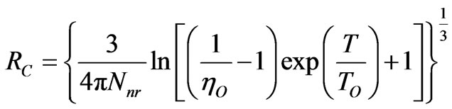
Dunstan and Boulitrop [24] dealt with the spatial position of the carrier relative to the point where it was first trapped. This position was determined by a random walk in which the steps have a distribution of positions. For each successive steps, this distribution shifts to larger values of position. This idea is different somewhat from the concept of the spatial confinement which was first proposed by Tiedje et al. [25] for thin layers. The position, in this case, was determined by not the random walk but by a limit volume. In the spatial confinement, the common model of recombination in the amorphous silicon was used which was suggested by Street [26] in which the defects provide the dominant recombination centers. The distance around the defect at which the nonradiative and radiative recombination rates are equal is defined as a nonradiative capture radius, RC [19]. Therefore; the capture volume can be regarded as a sphere surrounding the defect [25] .When the electronhole pair is inside the sphere, they recombines nonradiatively; otherwise, they recombines radiatively [19,25]. In this case, the electron-hole pairs can recombine either radiatively or nonradiatively. Then, the capture radius, RC, may be viewed as the characteristic length explored by a photocreated electron-hole pair before its radiative recombination [19]. In view of the fact that the values of RC must not be adopted randomly, an expression for the effective capture radius was derived that takes the form [19,21].
 (1)
(1)
where Nnr is volume nonradiative recombination density (cm−3), TO is an experimentally determined constant and  is the low temperature maximum quantum efficiency limit. RC is considered as a characteristic length for this case. The consequence of spatial confinement effect is the localization of electrons and holes inside small size that leads to reflections or folding of phonons in k-space [27].
On the other hand, a characteristic length is considered the de Broglie wavelength for the quantum confinement case. According to the effective mass approximation, electrons and holes in a semiconductor are described as independent particles with an effective mass,  and
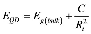
and  respectively. They can be determined by the convexity of the band edge structure. Both the electron states in the conduction band and the hole states in the valence band are quantized, where the 1s electron state increases in energy with decreasing the radius dot, R, while the 1 s hole state decreases [8]. By using the best fitting for the experimental data that is achieved by Park et al. [15], this effect is carried out in the a-SiQDs model. According to effective mass theory, an infinite potential barrier is assumed, thus, the energy gap,
  , for a three-dimensionally confined a-SiQDs model is expressed as [13-15].
 (2)
(2)
where 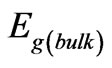 is the bulk band gap of the a-Si that takes the value (1.56 eV) obtained from the best fitting for the experimental data, which has been mentioned above. This value is very close to the values reported in literature for bulk a-Si [(1.5 - 1.6) eV] [28]. Rt is the radius of the dot and C is the confinement parameter which is estimated to be about (2.4 eV nm2). Since the
 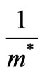 is included in the confinement parameter,
  where
where  and
and  are the electron and hole effective masses respectively. On contrast of assumption of Park et al., it was assumed [15] that the effective masses are not isotropic for three directions in amorphous silicon. However, quantum confinement theory predicts that the band gap in a-SiQD opens with decreasing dot size. The quantum confinement causes an increase of the band gap.
The type of transitions in this study is allowed to be indirect transitions, as is normally done with bulk amorphous silicon. The absorption coefficient of amorphous silicon can be obtained from Taus expression in the photon energy range  [29]:
[29]:
 (3)
(3)
here  is a constant related to the amorphous silicon material.
  takes the value of energy gap in bulk case for the spatial confinement, while it has the value of
  for the quantum confinement.
The chance that a tail state receives a carrier thermalizing from above (or below) is independent of its energy. The probability of thermalized carriers in one tail state is determined by the local configuration of other tail states, both above it and below it [24]. On the other hand, each tail state has a very different probability of losing a carrier to deeper states; this probability is determined by the local arrangement of deeper state and is strongly correlated to the energy of the state. However, such dependence could be accounted for by a dominant hopping process through which the carriers thermalize in deeper energy tail states [30]. The rate of hopping is proportional to the density of localized states which are involved in the thermalization [31].
In this model, the same recombination process is active in both a-SiQDs and bulk a-Si [32].These processes take place, without Stokes Shift, via tunneling between the deepest accessible energy conduction and valence states in the respective band tail [11,18,19]. Radiative transition to/or from defect levels near midgap is not considered here because this transition does not occur at only one band [18,21]. In addition the surface transitions do not make additional radiative recombination paths [25]. This process always occurs with the nearest neighbor because of it’s strong dependence on R [26]. Therefore, we assumed that any electron-hole pair created within the distance ( when
when  and
and  when
when ) will recombine nonradiatively. If the electron-hole pair is created farther than this distance, it will recombine radiatively. In addition, it was suggested [18] that the surface states play no important roles in the recombination process. Nonradiative recombination occurs through tunneling to a nonradiative defect center when such a center is within the capture volume,
 . We have assumed that the surface is an additional nonradiative state due to excess dangling bond. It is important to note that in a-SiQDs structure, carriers will find the deepest energy paths within the volumes of spheres. While in bulk, carriers may recombine through only a few low energy tail or defect [18].
In general, the recombination process depends on the tunneling type, tunneling distance and tunneling time. Tunneling can be either a radiative or a nonradiative process [19], and the principal distinction between them is the value of tunneling attempt rate,  , which is about (108 sec−1) for radiative process [18,24]. It may be useful to mention that, the radiative process occurs to carriers in the other band [24]. But; nonradiative transition,
  is between [(1012 - 1013) sec−1] [18,33], and it happens in deepest tail states of the same band [24]. The average tunneling time, τ, for an electron and a hole separated by a distance, R, is given by [18,26]:
 (4)
(4)
In this equation  is the tunneling attempt rate
  and
and  is the effective Bohr radius. According to Street [26] this expression is valid for
 . It should be noted that the tunneling transitions probability (τ−1) depends exponentially on the pair separation [24]. For bulk case, Tiedje et al. [25] assumed that typical tunneling distance for electrons and holes is equal to a nonradiative capture radius,
 . But, in our model, the assumption that estimates the average tunneling distance to be roughly equal to the a-SiQDs sphere radius
  is adopted [18].
3. Results and Discussion
An important consequence of quantum confinement is the increase in the band gap as the quantum dot size is decreased [34,35]. Since the wavefunction of carriers is strongly localized within the quantum dot [32], the effect of quantum confinement might cause the spreading of the band tail state in a-SiQDs, which is due to the quantum confinement carriers, rather than the increase of structural disorder [29]. It is important to mention that the existence of localized states is believed to be less sensitive to quantum confinement [16,33].
Each size has a magnitude for the energy gap which results from the quantum treatment. It is noted that the energy gap magnitude (1.56 eV for bulk) increases with the decrease of the size. The cause of this behavior is that from the energy levels have moved to higher energies depending on the size. Thus, the energy gap of one size is different from the other. On the other hand, the spatial confinement effect increases with the decrease of quantum dot size. In fact, this is in agreement with the first suggestion of spatial position, but not by a random walk of steps. It is clarifying the principle of spatial confinement that is suggested by Tiedje et al. From this, it can be said that the spatial confinement may occur at any size with the quantum confinement (below the bulk-like size).
Figure 1 illustrates the absorption coefficient for spatial confinement case as a function of the emitted photon energy. The absorption coefficient is appropriated with the size of quantum dot, where  decreases as the dot size decreases. The reason for this behavior is related to the effective excitation cross section that decreases with the decrease of the dot size [36,37]. Since the cross section deceases, the density of excitation states, and accordingly the carriers that may exist in these states decrease too. On the other hand, the absorption energy also decreases with the decrease of dot size. This energy can be shifted towards a longer wavelength (red shifting). Figure 1 shows the absorption coefficient for combination of all the sizes used in this work. It is clear from the figure that the absorption coefficient of the spatial confinement has the same behavior as in the bulk case, which is distinguished as a continuous spectrum.
In the case of quantum confinement, the behavior of the absorption coefficient is different, as shown in Figure 2, with the same sizes used in the case of the spatial confinement ( in this case , the equation used (3) is also with  which is different from size to another). In fact, the decrease in
  with the decrease of the dot size can be attributed to the same reason mentioned in the case of spatial confinement. While, the behavior of absorption energy differs from that of the previous case, where it is shifted to the shorter wavelength (blue shifting).
The absorption spectrum of a-SiQDs consists of a series of discrete lines as indicated in Figure 2. The con-
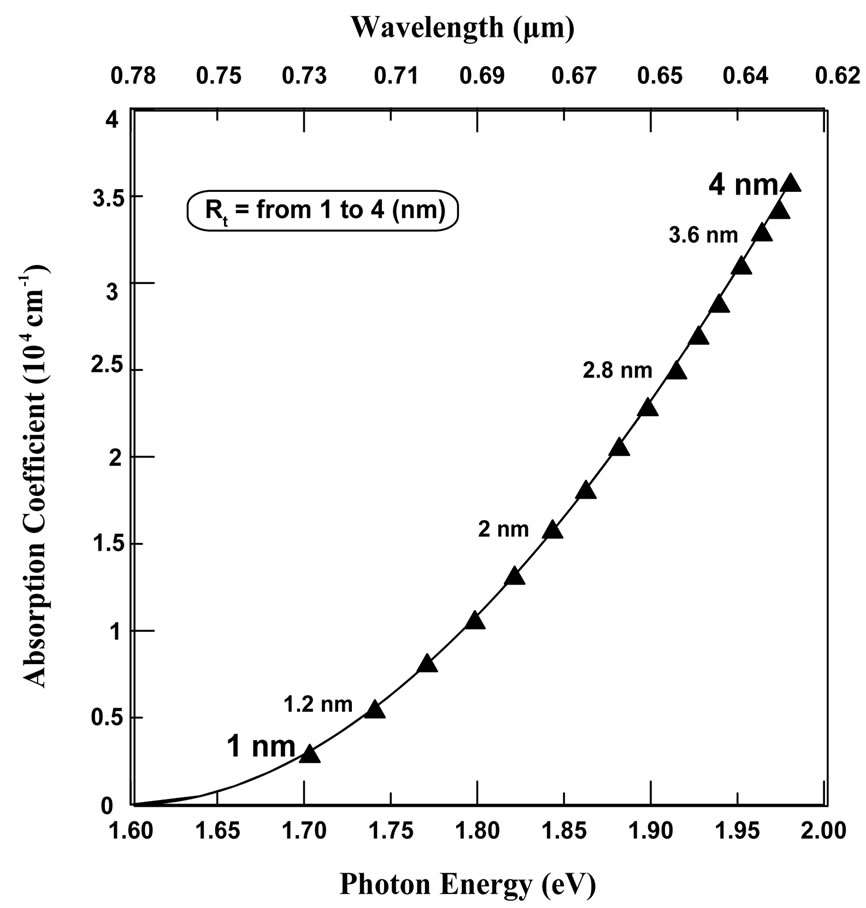
Figure 1. The absorption coefficient for all sizes as a function of photon energy as a continuous spectrum.
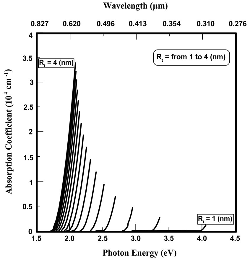
Figure 2. The absorption coefficient for all sizes at the quantum confinement as a series of discrete lines.
fining electrons in a-SiQD produce a series of even sharper spikes which corresponds to a series of confinement quantum levels for these electrons, where the quantum dots absorb all wavelengths shorter than the absorption maximum (~Eg) [38]. Also, it is noted that the threshold of absorption is shifted by several electron volts from that of the bulk. As it can be seen from the figure, the difference in energy for each two successive sizes increases excessively as the size reduces. It is important to note that, the differences between two small sizes allow a good active area in the search.
The enhancement of radiative recombination results from a confinement effect, which is considered as one of the most effective means to convert an indirect optical transition into a direct [9]. It is found [12] that; the rate of radiative recombination is expressed as:
 (5)
(5)
where  is defined in equation (4). Figure 3 illustrates the rate of the radiative recombination as a function of quantum dot size for our model. Generally, it can be seen from this figure that the number of the carriers, which are recombined radiatively, is increasing by decreasing the quantum dot size. This evidence indicates that a large number of tunneled carriers can recombine radiatively. While, in the large size only a small ratio of those carriers can recombine radiatively. In fact, the probability of radiative recombination depends on the local arrangement of carriers in the other band [24]. In other words, the transitions between the two bands are increases when
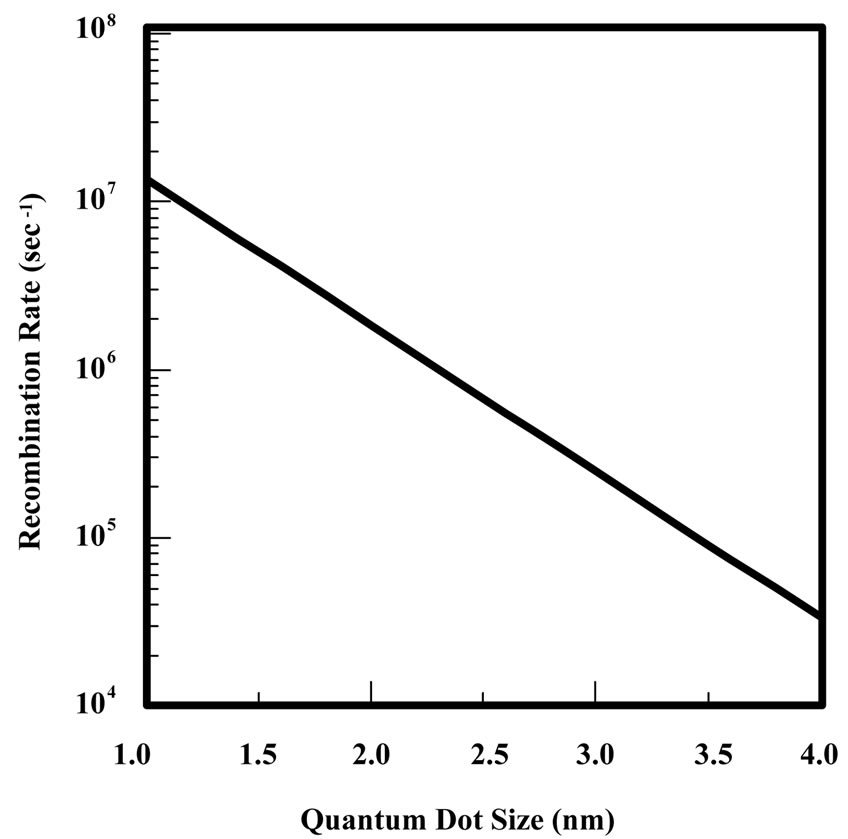
Figure 3. The rate of the radiative recombination as a function of the quantum dot size.
the size is reduced.
The mechanism of transitions in the present a-SiQDs model may be considered to understand the dynamic of confinement. It is well known, that in bulk crystal of indirect gap materials, the electron-hole recombination is possible only through phonon emission or phonon absorption. This because the wave-vector difference between the conduction-band bottom and the valence-band top must need to be compensated. However, in the quantum mechanics theory, the radiative transitions of electromagnetic waves with determination of their frequency, are due to Bohr's law, while the allowed transitions are due to the selection rule (n2 − n1 = 1) [39]. When the dot size is decreased the conduction-band bottom becomes more convex, while the valence-band top becomes more flat. This behavior will decrease the electron effective mass (at conduction band), and increases the hole effective mass (at the valence band) [40]. As mentioned previously the quantum dots behave as molecules, therefore, each dot can be expressed as a harmonic oscillator, where the energy can be obtained by:
 (6)
(6)
here  is the frequency of vibration that is given by
 ,
,  being the force constant. This energy represents the phonon energy and its frequency is equal to the frequency of the oscillator, which has the same mass, and the same force constant at allowed transitions. Consequently, the conduction band bottom is folded on Г point [40], thus, Δk is folding too. On the other hand, the emitted photons result from the transitions that occur from the conduction band to valence band (which are due to Bohr’s law). In these transitions, the energy of emitted photon decreases when the dot size decreases (red shifting).
The dynamic of quantum confinement for present model is characterized by the shifting of energy levels of both conduction and valence bands. This shifting is proportional to the dot size, where the carriers are confined in three-dimensions, in the case of quantum dots. This leads to the overlap of the envelope wavefunctions, which is more than in the other nanostructures. However, the shifting of energy levels becomes more when the dot size decreases. This can be explained as following: As the dot size decreases the effective mass of electron (hole) decreases (increases), therefore; the energy levels are shifted to higher (lower) magnitude of conduction (valence) band, which results from the assumption of
 . For this reason, the energy gap has different values depending on the dot size. By applying Bohr's law in this case, the photon energy for each size has unique value, where it increases as the dot size decreases (blue shifting).
In fact, the origin of quantum confinement is known to arise from the spatial confinement of carriers within the quantum dot boundary [34]. This means that the spatial confinement coexists with the quantum confinement. Since the spatial confinement of carriers inside a quantum dot is the reflecting or the folding of phonons in the k-space when the dot size decreases, the energy levels will shift to higher (lower) magnitude for conduction (valence) band by the quantum confinement. This relaxes the k-conservation requirement and creates a quasi-direct band gap.
Figure 4(a), (from left to right), illustrates the effect of spatial confinement for different sizes of the dots, (decreasing in the size of dots). It is noted that the role of effective mass is closed and broad the conduction band and the valence band respectively with no change in the energy gap. While Figure 4(b) shows the widening of the energy gap for different sizes of the dots. Finally, Figure 4(c) depicts the combination effects of both confinements (spatial and quantum) for the same sizes of dots and we have direct transition.
4. Conclusions
In conclusion, the optical energy gap transition of a-Si has been changed from indirect to direct transition by adopting the a-Si as quantum dot with very low radius
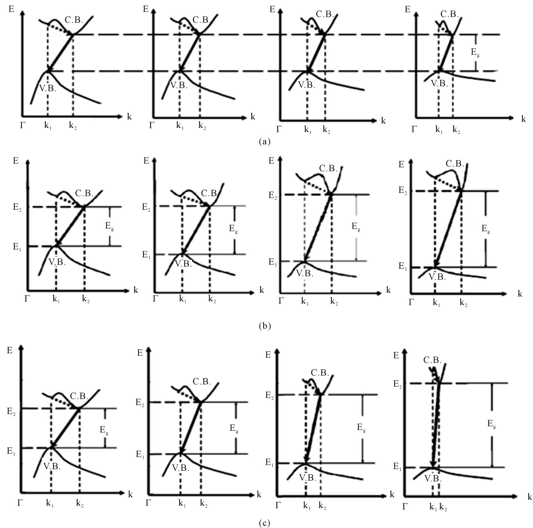
Figure 4. From left to right: (a) The effect of spatial confinement with the decreasing of the dot size; (b) the effect of quantum confinement with the decreasing of the dot size; (c) the effect of both spatial and quantum confinement with the decreasing of the dot size.
dimension (<1.8 nm). This is happened when spatial and quantum confinement’s effects are taken both in consideration. Also, a continuous shifting toward low energy (red shift) and toward high energy (blue shift) with the decreasing of the quantum dot size are due to the existence of both spatial and quantum confinements respectively.
5. Acknowledgements
We thank Dr. Ahlam H. Al-Mousawy, for her useful discussions.
REFERENCES
- J. Koga, K. Nishio, T. Yamaguchi and F. Yonezawa, “Tight-Binding Electronic State Calculations of Silicon Nanostructures with Local Disorders: Origin of the F Band Luminescence from Porous Silicon,” Journal of the Physical Society of Japan, Vol. 70, No. 8, 2001, pp. 2478-2484. doi:10.1143/JPSJ.70.2478
- J. Koga, K. Nishio, T. Yamaguchi and F. Yonezawa, “The Effects of the Point-Group Symmetry in Silicon Nanostructures on Radiative Recombination Time,” Journal of the Physical Society of Japan, Vol. 70, No. 10, 2001, pp. 3143-3148. doi:10.1143/JPSJ.70.3143
- F. Yonezawa, K. Nishio, J. Koga and T. Yamaguchi, “Theoretical Prediction for Realization of Spectra-controllable High-Efficient Photoluminescent Devices by Means of Silicon Nanostructures,” Journal of the Optoelectronics and Advanced Materials, Vol. 4, No. 3, 2002, pp. 569-574.
- C. J. Murphy and J. L. Coffer, “Quantum Dots: A Primer,” Focal Point, Vol. 56, No.1, 2002, pp. 16A-26A.
- T. F. Jiang, X. Tong and S. Chu, “Self-Interaction-Free Density Functional Theoretical Study of the Electronic Structure of Spherical and Vertical Quantum Dots,” Physical Review B, Vol. 63, 2001, pp. 045317-1-045317-9.
- Y. Alhassid, “The Statistical Theory of Quantum Dots,” Reviews of Modern Physics, Vol. 72, No. 4, 2000, pp. 895-968. doi:10.1103/RevModPhys.72.895
- J. S. Williams, R. G. Elliman, H. H. Tan, P. Lever, J. Wong-Leung and C. Jagadish, “Production and Processing of Semiconductor Nanocrystals and Nanostructures for Photonic Applications,” Materials Forum, Vol. 26, 2002, pp. 74-80.
- C. Kittle “Introduction to Solid State Physics,” 8th Edition, John Wiley& Sons, Hoboken, 2004.
- T. Toyama, Y. Nakai, A. Asano and H. Okamoto, “Optical Transitions in Silicon Nanocrystals near Structural Transition Region to Amorphous Silicon,” Journal of Non-Crystalline Solids, Vol. 299-302, 2002, pp. 290-294. doi:10.1016/S0022-3093(01)01006-7
- I. Sychugov, R. Juhasz, A. Galeckas, J. Valenta and J. Linnros, “Single Dot Optical Spectroscopy of Silicon Nanocrystals: Low Temperature Measurements,” Optical Materials, Vol. 27, No. 5, 2005, pp. 973-979. doi:10.1016/j.optmat.2004.08.046
- K. Nishio J. Koga, T. Yamaguchi and F. Yonezawa, “Light Emission Properties of Amorphous Silicon Quantum Dots,” Journal of Non-Crystalline Solids, Vol. 312- 314, 2002, pp. 323-326. doi:10.1016/S0022-3093(02)01705-2
- K. Nishio J. Koga, T. Yamaguchi and F. Yonezawa, “Theoretical Study of Light-Emission Properties of Amorphous Silicon Quantum Dots,” Physical Review B, Vol. 67, No. 19, 2003, pp. 195304-1-195304-5. doi:10.1103/PhysRevB.67.195304
- H.-S. Kwach, Y. Sun, Y.-H. Cho, N.-M. Park and S.-J. Park, “Anomalous Temperature Dependence of Optical Emission in Visible-Light-Emitting Amorphous Silicon Quantum Dots,” Applied Physics Letters, Vol. 83, No. 14, 2003, pp. 2901-2903.
- N.-M. Park, T.-S. Kim and S.-J Park, “Band Gap Engineering of amorphous silicon quantum dots for LightEmitting Diodes,” Applied Physics Letters, Vol. 78, No. 17, 2001, pp. 2575-2577. doi:10.1063/1.1367277
- N.-M. Park, C.-J. Choi, T.-Y. Seong and S.-J. Park, “Quantum Confinement in Amorphous Silicon Quantum Dots Embedded in Silicon Nitride,” Physical Review Letters, Vol. 86, No. 7, 2001, pp. 1355-1357. doi:10.1103/PhysRevLett.86.1355
- T.-W. Kim, C.-H. Cho, B.-H. Kim and S.-J. Park, “Quantum Confinement Effect in Crystalline Silicon Quantum Dots in Silicon Nitride Grown Using SiH4 and NH3,” Applied Physics Letters, Vol. 88, No. 12, 2006, pp. 123102-1-123102-3. doi:10.1063/1.2187434
- S. M. Sze, “Semiconductors Devices Physics and Technology,” 3rd Edition, John Wiley & Sons, Inc., Hoboken, 2007.
- M. J. Estes and G. Moddel, “Luminescence from Amorphous Silicon Nanostructures,” Physical Review B, Vol. 54, No. 20, 1996, pp. 14633-14641. doi:10.1103/PhysRevB.54.14633
- Y. kamemitus,Y. Fukunishi and T. Kushida, “Decay Dynamic of Visible Luminescence in Amorphous Silicon Nanoparticles,” Applied Physics Letters, Vol. 77, No. 2, 2000, pp. 211-213. doi:10.1063/1.126927
- S. A. Maksimenko, G. Y. Slepyan, N. N. Lrdentsove, V. P. Kalosha, A. Hoffmann and D. Bimberg, “Light Confinement in Quantum Dots,” 8th International Symposium on Nanostructures: Physics and Technology, St Petershurg, June 19-23 2000, pp. 219-223.
- M. J. Estes and G. Moddel, “A Model of Size-Dependent Photoluminescence in Amorphous Silicon Nanostructures: Comparison with Observations of Porous Silicon,” Applied Physics Letters, Vol. 68, No. 13, 1996, pp. 1814- 1816. doi:10.1063/1.116022
- J. M. Martinez-Duart, R. J. Martin-Palma and F. AgulloRueda, “Nanotechnology for Microelectronics and Optoelectronics,” Elesvier, Amsterdam, 2006.
- N.-M. Park, S.-H. Jeon, H.-D.Yung, H.Hwang, S.-J. Park and S.-H. Choi, “Size-Dependent Charge Storage in Amorphous Silicon Quantum Dots Embedded in Silicon Nitride,” Applied Physics Letters, Vol. 83, No. 5, 2003, pp. 1014-1016. doi:10.1063/1.1596371
- D. J. Dunstan and F. Boulitrop, “Photoluminescence in Hydrogenated Amorphous Silicon,” Physical Review B, Vol. 30, No. 10, 1984, pp. 5945-5957.
- T. Tiedje, B. Abeles and B. G. Brooks, “Energy Transport and Size Effects in the Amorphous-Silicon Multilayer Structures,” Physical Review Letters, Vol. 54, No. 23, 1985, pp. 2545-2547. doi:10.1103/PhysRevLett.54.2545
- J. I. Pankove, “Semiconductors and Semimetals Hydrogenated Amorphous Silicon Part B, Optical Properties,” Academic Press, Cambridge, 1984.
- M. A. Green and G. Conilbeer, “Silicon Quantum Dot Based Solar Cells: Addressing the Issues of Doping, Voltage and Current Transport,” 25th European Photovoltaic Solar Energy Conference and Exhibition/5th World Conference on Photovoltaic Energy Conversion, Valencia, 6-10 September 2010, pp. 182-190.
- K. Tanaka, E. Moruyama, T. Shimada and H. Okamoto, “Amorphous Silicon,” John Wiley & Sons Ltd., Hoboken, 1999.
- J. Tauc, “Amorphous and Liquid Semiconductors,” Plenum, New York, 1974.
- F. Giorgis, C. F. Pirri, C. Vinegoni and L. Pavesi, “Luminescence Processes in Amorphous Hydrogenated Silicon-Nitride Nanometric Multilayers,” Physical Review B, Vol. 60, No. 16, 1999, pp. 11572-11576. doi:10.1103/PhysRevB.60.11572
- S. Kivelson and C. D. Gelatt Jr., “Photoluminescence in a Disordered Insulators the Trapped-Exciton Model,” Physical Review B, Vol. 26, No. 8, 1982, pp. 4646-4673. doi:10.1103/PhysRevB.26.4646
- Y. kamemitus,Y. Fukunishi and T. Kushida, “Decay Dynamics of Visible Luminescence in Amorphous Silicon Nanoparticles,” Applied Physics Letters, Vol. 77, No. 2, 2000, pp. 211-213.
- B. Abeles and T. Tiedje, “Amorphous Semiconductor Superlattices,” Applied Physics Letters, Vol. 51, No. 21, 1983, pp. 2003-2005. doi:10.1103/PhysRevLett.51.2003
- K. E. Anderson, C. Y. Fong and W. E. Pickett, “Quantum Confinement in CdSe Nanocrystallites,” Journal of NonCrystalline Solids, Vol. 299-302, 2002, pp. 1105-1110.
- A. Dumbrava, V. Ciupina and G. Prodan, “Dependence on Grain Size and Morphology of Zinc Sulfide Particles by the Synthesis Rout,” Romanian Journal of Physics, Vol. 50, No. 7-8, 2005, pp. 831-836.
- N.-M. Park, T.-Y. Kim, G. Y. Sung, B.-H. Kim, S.-J. Park, K. S. Cho, J. H. Shin, J.-K. Lee and M. Nastasi, “The Dot Size Effect of Amorphous Silicon Quantum Dot on 1.54 µm Er Luminescence,” Proceeding of Materials Research Society Symposium, Vol. 817, 2004, pp. L1.4.1-L1.4.6.
- N.-M. Park, T.-Y. Kim, K.-H. Kim, G. Y. Sung, B.-H. Kim, S.-J. Park, K. S. Cho, J. H. Shin, J.-K. Lee and M. Nastasi, “Effect of Amorphous Si Quantum-Dot Size on 1.54 µm Luminescence of Er,” Journal of Electrochemical Society, Vol. 152, No. 6, 2005, pp. G445-G447. doi:10.1149/1.1901662
- W. G. J. H. M. Sark, C. De M. Donega, C. Harkisoen. R. Kinderman, J. A. M. van Roosmalen, R. E. I. Schropp and E. H. Lysen, “Improvement of Spectral Response of Solar Cells By Deployment of Spectral Converters Containing Semiconductor Nanocrystals,” Solar Energy Material & Solar Cells, Vol. 87, 2005, pp. 395-409.
- M. Jaros, “Physics and Applications of Semiconductor Microstructures,” Clarendon Press, Oxford, 1989.
- T. Takagahara and K. Takeda, “Theory of the Quantum Confinement Effect on Excitons in Quantum Dots of Indirect-Gap Materials,” Physical Review B, Vol. 46, No.23, 1992, pp. 15578-15581. doi:10.1103/PhysRevB.46.15578