Journal of Modern Physics
Vol. 2 No. 7 (2011) , Article ID: 5790 , 5 pages DOI:10.4236/jmp.2011.27083
Exciton Dynamics in Stacked InGaAs/GaAs Quantum Rings under Resonant Excitation
1Université Carthage, Tunis, Tunisie.
2Universidad de Valencia, Valencia, Spain.
3Instituto de Microelectrónica de Madrid, Madrid, Spain.
E-mail: Ouerghuiwalid@yahoo.fr
Received March 5, 2011; revised April 20, 2011; accepted May 3, 2011
Keywords: Quantum Rings, Vertical Stacks, Carrier Tunnelling
ABSTRACT
We report systematic temperature-dependent measurements of photoluminescence spectra in self-assembled InGaAs/GaAs quantum rings (QRs) under resonant excitation condition. We have studied the rise in temperature of the ground-state intensity. The carrier transfer between the ground state of the small ring family towards the big-ring family of the bimodal size distribution is identified by analyzing the photoluminescence spectra. This effect is observed in very thin spacer and under resonant excitation. This situation makes important the lateral tunneling of excitons between rings under low temperatures (10 K). Tunneling time about 1ns was estimated at low temperature and compared to similar carrier transfer in quantum dots (QDs) found in the literature.
1. Introduction
Due to the increasing potential applications of semiconductor quantum nanostructures like quantum dots (QDs) and quantum rings (QRs) for the development of room temperature operating hetero-structure lasers and high- speed optoelectronic devices, the carrier tunneling and thermal escape processes are of considerable interest [1-3]. In particular, self-assembled QRs of InGaAs grown on GaAs are potential candidates for the development of laser diodes at 980 nm at room temperature and high-speed optoelectronic devices. Stacked layers of QR have been grown for different GaAs spacers, demonstrating the laser operation in the most favourable cases [4]. The QR system allows a great density of multilayer stacks, because of their reduced height, more than three times smaller than typical QD, while avoiding excessive electronic coupling. The lateral tunneling of exciton is one of the most important dynamic features in semiconductors, since it contains directly the information about localization effects between excitons and their environment. In this domain, the tunneling time is determined from time resolved experiment and theoretical models, and then it can be deduced [2,5,6].
For lateral carrier tunneling we find the results reported in reference [2], where a value of around 3.5 ns is found for “carrier transfer” in high density QD arrays from small dots emitting at around 1.3 eV towards bigger dots emitting at lower energies. In our previous work [6], using both a theoretical model and time resolved experiment; we find that the tunneling time is about 5 ns. In the present paper, we employ another method to deduce the tunneling time in QR.
We demonstrate that in a very thin spacer, 1.5 nm, the recombination dynamics is affected by the lateral tunneling of carriers between QR at tow temperature, and we deduce the value of tunneling time, between the ground state of the small ring family towards the big-ring family of the bimodal size distribution, of about 1 ns using photoluminescence experiment under resonant excit- ation conditions.
2. Samples and Experiment
The sample studied in this work follow a similar growth procedure. An initial QD seeding layer is grown by depositing 1.7 monolayer (ML) of InAs onto a (001)-GaAs substrate (after a GaAs buffer layer) at 540˚C, under an As2 beam equivalent pressure of (3 – 4) × 10−6 mbar. The InAs deposition takes place in a growth sequence of 0.1ML InAs (at 0.06 ML/s) plus a 2 s pause under As flux. At the end of this sequence, the QDs are annealed 1 min to enhance the size distribution and to obtain medium density ensembles (109 - 1010 cm−2). Subsequently, a thin GaAs cap layer is grown (at a rate of 1 ML/s) at different atmospheres and substrate temperatures, TCAP. In this way, QR are obtained under As2 atmosphere at 1.1 × 10⁻⁶ mbar and TCAP = 500˚C.
More details about the growth of this kind of sample can be found in ref [7,8]. The sample studied here contains three layers of QR stacked by using 1.5 nm GaAs spacer thickness. In each layer, the total amount of deposited InAs was just above the critical thickness (1.6 ML) necessary for the 3D transition to take place, which induces low in-plane densities of nanostructures. The typical size of the original dots was around 20 - 40 nm diameter and around 11 nm of height, in average. The presence of QR nanostructures in these stacks have been revealed and studied by Atomic Force Microscopy (AFM), Transmission Electron Microscopy (TEM) [8] and Scanning Tunneling Microscopy (STM) [9]. From AFM, typical dimensions obtained for QR are 100 nm ´ 90 nm ´ 1.5 nm. From TEM and STM, more morphological and compositional information is obtained for QR. In particular, the QR has not a homogeneous composition, as expected from its formation process, in which 2 nm of GaAs is used to partially cap the seed pyramidal dots. In this way, the central part of the ring, around 20 nm in diameter, is pure InAs, whereas the outer zone of the ring (up to the 100 nm of diameter typically measured by AFM) have a variable compositional profile of InGaAs due to the initial alloying effect of the original InAs dot and the 2 nm thick GaAs capping layer [8,9].
The continuous wave photoluminescence (cw-PL) experiment was performed by using the 514 nm Ar+ line pumped continuous wave Ti: sapphire laser for excitation. The PL signal was dispersed by a single 0.5 m focal length monochromator and synchronously detected with a cooled Ge detector. The sample was held in the cold finger of a closed-cycle cryostat to vary the temperature in the range 12 - 300 K, approximately.
3. Results and Discussions
Figure 1 shows the PL spectra measured at low temperature and using above barrier (GaAs) and low density excitation under resonant excitation (880 nm) conditions. The PL spectra can be reasonably deconvoluted into two Gaussian components, as shown in Figure 1, which are separated by around 52 MeV. The parameters of these Gaussian components are labelled as P1 (high energy component) and P2 (low energy component).
First of all, the two observed PL Gaussian components cannot be due to the contribution of excited states of a

Figure 1. The PL spectra measured at low temperature and using above barrier (GaAs) and low density excitation under resonant excitation (880 nm) conditions.
mono-modal QR size distribution; because when we use higher excitation densities we can perfectly observe that contribution (p-like exciton recombination) on the high energy side of the PL spectra. We attribute the measured PL band to a bi-modal size distribution of the QR ensemble (i.e., two different size families), being similar in each of the three stacked layers, in average. The measured energy separation between the two QR families (23 - 27 MeV), under non resonant excitation, is approximately consistent with an average height fluctuation of 0.3 nm (one monolayer) [10-12].
Figure 2 plots the temperature dependence of the PL intensity at excitation density of 3.14 W/cm2 and under resonant excitation. The two Gaussian contributions (P1-P2) representative of the QR ensemble are followed with increasing the temperature. Above 90 K the PL band is practically symmetrical (single Gaussian), because of the negligible influence of P2 on its low energy side.
At low temperatures (10 - 40 K), the PL energy associated to the small QR is quite stable, then decrease for higher temperature (see inset of Figure 3). The peak energy P1 shows a displacement towards low energy (red shift). Such behavior is characteristic for escapement of carriers from the small ring family (P1). Whereas in the temperature range (10 - 60) K the peak energy (P2) which associated to the big ring family is increased, then decrease for higher temperature (>60 K). This effect is due to a transfer from the high energy (P1) band towards the low energy band (P1). This process can be possible by phonon assisted tunneling from the small-ring towards the big ring.
Figure 3 shows the Arrhenius plot of the integrated PL intensity for both P1 and P2 components in the sample under low excitation density conditions. The best fitting of the experimental results is shown in Figure 3(a) and (b) as
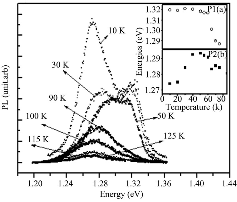
Figure 2. The temperature dependence of the PL intensity at excitation density of 3.14 W/cm2 and under resonant excitation
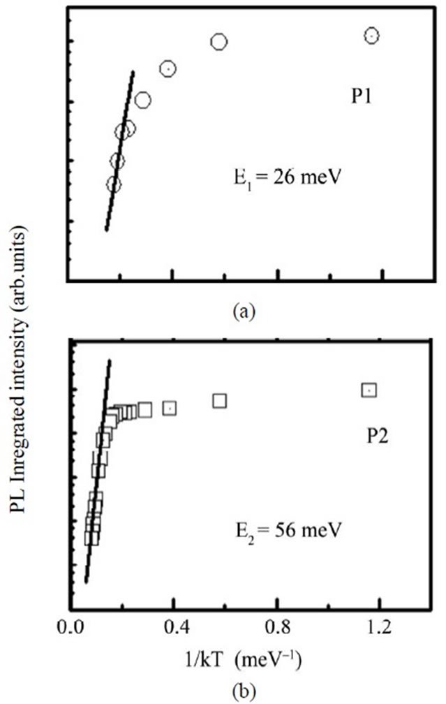
Figure 3. The Arrhenius plot of the integrated PL intensity for both P1 and P2 components in the sample under low excitation density conditions.
a continuous line, by using E1 = 26 ± 5 meV and E2 = 56 ± 5 MeV. The activation energy E1 is close to the GaAs (or InAs confined) LO phonon energy, but also to the half of the energy difference between P1 and P2 ring families (their average ground status). The activation energy found suggests the existence of a thermal activated carrier transfer mechanism from P1 towards P2 rings. The origin of such inter-ring (P1 - P2) carrier transfer would be a non-resonant tunneling process assisted by optical phonons, as suggested in [3,5,13,14]. It is worth noting that the temperature at which the tunneling effect begins (i.e., the process of carriers transfer between QR families begin), 10 K, is much smaller than that found for QR (T  40 K) in [3]. The most likely transfer mechanism, phonon assisted tunneling, is thus significantly stronger for QR with thin GaAs spacer. The main differences in the carrier transfer between QR with thin spacer and the results found in [3] are associated to the thin spacer heterostructures used where we can imagine that the three QR layers can be accounted for by multiplying also by three the tunneling probability.
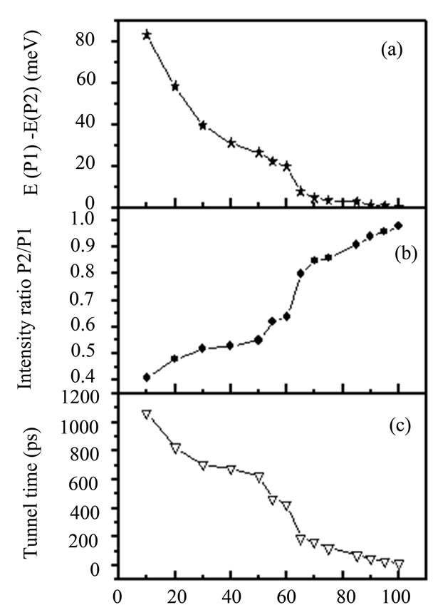
Figure 4 shows the obtained temperature dependence of tunneling time τT within the PL band in QR sample. Following [15], we have calculated τT by means of the relation . With η is the intensity ratio P2/P1 and τS is the time characteristic of the radiative recombination on the ground state of the quantum rings which is about 765 ps [6]. For T = 10 K, the estimated τT is ≈ 1064 ps whereas for high temperature, τT decrease.
Value around 3.5 ns have been reported for nonresonant electron tunneling for “carrier transfer” in high density QD arrays from small dots emitting at around 1.3 eV towards bigger dots emitting at lower energies [2]. For lateral carrier tunneling in QR ( using both theoretical model and time resolved experiment) we find in the results reported in [6], where a value of around 5 ns is found for “carrier transfer” between the ground state of the small ring family towards the big-ring family of the bimodal size distribution.
In the present paper, we employ another method to deduce the tunneling time in QR. Indeed, under resonant condition excitation, we have estimated the tunneling time τT around 1 ns. One can see in Figure 4.c, that τT sharply decreases and became smaller, at high temperature, than the ground-state life time indicating that the process of lateral tunneling begins to play a more essential role and became dominant at higher temperatures.
The physical reason for the important increase, at high temperature, of lateral tunneling between the ground state of the small ring family towards the big-ring family of the bimodal size distribution is that non-resonant tunneling process assisted by optical phonons is becoming increasingly more resonant. Indeed, at high temperature the average energy difference between QRs family is about 26 meV (Figure 4(a)), value which is close to the LO phonon energy. In this case, the non-resonant tunneling process assisted by optical phonons must be significantly higher.
The resonant excitation conditions seems appropriate to deduce the realist tunneling time due to exciton transfer between different size distributions in self assembled in InGaAs//GaAs QRs.
Temperature (K)
Figure 4. The obtained temperature dependence of tunneling time τT within the PL band in QR sample.
4. Conclusions
In this paper we have studied stacked InGaAs quantum ring layers, separated by thin GaAs barriers, by means of steady state photoluminescence under very low excitation density and resonant excitation conditions. We have estimated the time for lateral carrier tunneling in stacked InGaAs QRs. The lateral transfer became efficient with increasing temperature and in consequence a decrease of tunneling time. We have uncovered a more complete picture of carrier transfer in multimodal QRs system, which will provide measures for greater control of PL behaviors.
REFERENCES
- S. Sanguinetti, M. Henini, M. G. Alessi, M. Capizzi, P. Frigeri, and S. Franchi, “Carrier Thermal Escape and Retrapping in Self-Assembled Quantum Dots,” Physical Review B, Vol. 60, No. 11, 1999, pp. 8276-8283. doi:10.1103/PhysRevB.60.8276
- J. W. Tomm, T. Elsaesser, Yu. I. Mazur, H. Kissel, G. G. Tarasov, Z .Y. Zhuchenko and W. T. Masselink, ‘‘Transient Luminescence of Dense InAs/GaAs Quantum Dot Arrays,” Physical Review B, Vol. 67, No. 4, 2003, pp. 045326-045333. doi:10.1103/PhysRevB.67.045326
- W. Ouerghui, J. Martinez-Pastor , J. Gomis , A. Melliti , M. A. Maaref, D. Granados and J. M Garcia, “Effect of Carrier Transfer on the PL Intesity in Self-assembled InGaAs/GaAs Quantum Respectfully Yours, Ings,” The European Physical Journal A, Vol. 35, No. 3, 2006, pp. 159-163. doi:10.1051/epjap:2006088
- F. Suarez, D. Granados, M. L. Dotor and J. M. Garcia, “Laser Devices with Stacked Layers of InGaAs/GaAs Quantum Rings,” Nanotechnology, Vol. 15, No. 4, 2004, pp. 126-130. doi:10.1088/0957-4484/15/4/003
- Y. I. Mazur, X. Wang, Z. M. Wang, G. J. Salamo, M. Xiao and H. Kissel, “Photoluminescence Study of Carrier Transfer among Vertically Aligned Double-Stacked InAs/ GaAs Quantum Dot Layers,” Applied Physics Letters, Vol. 81, No. 13, 2002, pp. 2469-2471. doi:10.1063/1.1510157
- W. Ouerghui, J. Martinez-Pastor, J. Gomis, M. A. Maaref, D. Granados and J. M. Garcia, ‘‘Lateral Tunneling in Sta- cked InGaAs/ GaAs Quantum Rings,” European Physical Journal B, Vol. 54, No. 2, 2006, pp. 217-223. doi:10.1140/epjb/e2006-00444-x
- M. L. Dotor, M. Recio, D. Golmayo and F. Briones, “Photoluminescence Characterization of GaAs Quantum Well Laser Structure with AlAs/GaAs superlattices Wave Guide,” The European Physical Journal Applied Physics, Vol. 72, No. 12, 1992, pp. 5861-5866. doi:10.1063/1.351891
- D. Granados, J. M. García, T. Ben and S. I. Molina, ‘‘Vertical Order in Stacked Layers of Self-Assembled Quantum Rings on GaAs (001),” Applied Physical Letters, Vol. 86, No. 7, 2005, pp. 071918-071920. doi:10.1063/1.1866228
- P. Offermans, P. M. Koenraad, J. H. Wolter, D. Granados, J. M. García, V. M. Fomin, V. M. Gladilin and J. T. Devreese, “Atomic-Scale of Self-Assembled InGaAs Quantum Rings in GaAs,” Applied Physics Letters, Vol. 87, No. 13, 2005, pp. 131902-131904. doi:10.1063/1.2058212
- S. Taddei, M. Collocci, A. Vinattieri, P. G. Gucciardi, F. Bogani, S. Franchi, P. Frigeri, L. Lazzarini and G. Salviati, “Vertical Coupling Effect in Arrays of InAs Quantum Dots,” Physical Status Solidi A, Vol. 224, No. 2, 2001, pp. 413-417. doi:10.1002/1521-3951(200103)224:2<413::AID-PSSB413>3.0.CO;2-6
- S. Taddei, M. Collocci, A. Vinattieri, F. Bogani, S. Franchi, P. Frigeri, L. Lazzarini and G. Salviati, “Vetical coupling and Transitions Energies in Multilayer InAs/GaAs Quantum-dot Structures,” Physical Review B, Vol. 62, No. 15, 2000, pp. 10220-10225. doi:10.1103/PhysRevB.62.10220
- W. Jaskolski, M. Zielinski, G. W. Bryant, ‘‘Coupling and Strain Effects in Vertically Stacked Double InAs/GaAs Quantum Dots,” Acta Physica Polonica A, Vol. 106, No. 2, 2004, pp. 193-205.
- A. Takeuchi, T. Kuroda, K. Mase, Y. Nakata and N. Yokoyama, ‘‘Dynamics of Carrier Tunneling between Vertically Aligned Double Quantum Dots,” Physical Review B, Vol. 62, No. 3, 2000, pp. 1568-1571. doi:10.1103/PhysRevB.62.1568
- T. Nakaoka, J. Tatebayashi, Y. Arakawa and T. Saito, “Carrier Relaxation in Closely Stacked InAs Quantum Dots: Tight-Binding Approach,” The European Physical Journal A, Vol. 96, No. 1, 2004, pp. 150-154. doi:10.1063/1.1755857
- R. Heitz, I. Mukhametzhanov, P. Chen and A. Madhucar, “Exciton Transfer in Self-Orgonized Asymetric Quantum Dot Pairs,” Physical Review B, Vol. 58, No. 16, 1988, pp. 10151-10154. doi:10.1103/PhysRevB.58.R10151